EP1192505B1 - Methods for patterning polymer films, and use of the methods - Google Patents
Methods for patterning polymer films, and use of the methods Download PDFInfo
- Publication number
- EP1192505B1 EP1192505B1 EP00927984A EP00927984A EP1192505B1 EP 1192505 B1 EP1192505 B1 EP 1192505B1 EP 00927984 A EP00927984 A EP 00927984A EP 00927984 A EP00927984 A EP 00927984A EP 1192505 B1 EP1192505 B1 EP 1192505B1
- Authority
- EP
- European Patent Office
- Prior art keywords
- polymer
- stamp
- material surface
- modifying
- film
- Prior art date
- Legal status (The legal status is an assumption and is not a legal conclusion. Google has not performed a legal analysis and makes no representation as to the accuracy of the status listed.)
- Expired - Lifetime
Links
Images
Classifications
-
- H—ELECTRICITY
- H10—SEMICONDUCTOR DEVICES; ELECTRIC SOLID-STATE DEVICES NOT OTHERWISE PROVIDED FOR
- H10K—ORGANIC ELECTRIC SOLID-STATE DEVICES
- H10K71/00—Manufacture or treatment specially adapted for the organic devices covered by this subclass
- H10K71/621—Providing a shape to conductive layers, e.g. patterning or selective deposition
-
- G—PHYSICS
- G03—PHOTOGRAPHY; CINEMATOGRAPHY; ANALOGOUS TECHNIQUES USING WAVES OTHER THAN OPTICAL WAVES; ELECTROGRAPHY; HOLOGRAPHY
- G03F—PHOTOMECHANICAL PRODUCTION OF TEXTURED OR PATTERNED SURFACES, e.g. FOR PRINTING, FOR PROCESSING OF SEMICONDUCTOR DEVICES; MATERIALS THEREFOR; ORIGINALS THEREFOR; APPARATUS SPECIALLY ADAPTED THEREFOR
- G03F7/00—Photomechanical, e.g. photolithographic, production of textured or patterned surfaces, e.g. printing surfaces; Materials therefor, e.g. comprising photoresists; Apparatus specially adapted therefor
-
- B—PERFORMING OPERATIONS; TRANSPORTING
- B82—NANOTECHNOLOGY
- B82Y—SPECIFIC USES OR APPLICATIONS OF NANOSTRUCTURES; MEASUREMENT OR ANALYSIS OF NANOSTRUCTURES; MANUFACTURE OR TREATMENT OF NANOSTRUCTURES
- B82Y10/00—Nanotechnology for information processing, storage or transmission, e.g. quantum computing or single electron logic
-
- B—PERFORMING OPERATIONS; TRANSPORTING
- B82—NANOTECHNOLOGY
- B82Y—SPECIFIC USES OR APPLICATIONS OF NANOSTRUCTURES; MEASUREMENT OR ANALYSIS OF NANOSTRUCTURES; MANUFACTURE OR TREATMENT OF NANOSTRUCTURES
- B82Y40/00—Manufacture or treatment of nanostructures
-
- G—PHYSICS
- G03—PHOTOGRAPHY; CINEMATOGRAPHY; ANALOGOUS TECHNIQUES USING WAVES OTHER THAN OPTICAL WAVES; ELECTROGRAPHY; HOLOGRAPHY
- G03F—PHOTOMECHANICAL PRODUCTION OF TEXTURED OR PATTERNED SURFACES, e.g. FOR PRINTING, FOR PROCESSING OF SEMICONDUCTOR DEVICES; MATERIALS THEREFOR; ORIGINALS THEREFOR; APPARATUS SPECIALLY ADAPTED THEREFOR
- G03F7/00—Photomechanical, e.g. photolithographic, production of textured or patterned surfaces, e.g. printing surfaces; Materials therefor, e.g. comprising photoresists; Apparatus specially adapted therefor
- G03F7/0002—Lithographic processes using patterning methods other than those involving the exposure to radiation, e.g. by stamping
-
- B—PERFORMING OPERATIONS; TRANSPORTING
- B41—PRINTING; LINING MACHINES; TYPEWRITERS; STAMPS
- B41C—PROCESSES FOR THE MANUFACTURE OR REPRODUCTION OF PRINTING SURFACES
- B41C1/00—Forme preparation
- B41C1/06—Transferring
-
- H—ELECTRICITY
- H10—SEMICONDUCTOR DEVICES; ELECTRIC SOLID-STATE DEVICES NOT OTHERWISE PROVIDED FOR
- H10K—ORGANIC ELECTRIC SOLID-STATE DEVICES
- H10K71/00—Manufacture or treatment specially adapted for the organic devices covered by this subclass
- H10K71/20—Changing the shape of the active layer in the devices, e.g. patterning
- H10K71/231—Changing the shape of the active layer in the devices, e.g. patterning by etching of existing layers
-
- H—ELECTRICITY
- H10—SEMICONDUCTOR DEVICES; ELECTRIC SOLID-STATE DEVICES NOT OTHERWISE PROVIDED FOR
- H10K—ORGANIC ELECTRIC SOLID-STATE DEVICES
- H10K85/00—Organic materials used in the body or electrodes of devices covered by this subclass
- H10K85/10—Organic polymers or oligomers
- H10K85/111—Organic polymers or oligomers comprising aromatic, heteroaromatic, or aryl chains, e.g. polyaniline, polyphenylene or polyphenylene vinylene
- H10K85/113—Heteroaromatic compounds comprising sulfur or selene, e.g. polythiophene
- H10K85/1135—Polyethylene dioxythiophene [PEDOT]; Derivatives thereof
Definitions
- the present invention concerns a method for patterning a polymer film forming a coating on a material surface, wherein the patterning takes place by means of a stamp having a surface with at least one indentation formed therein, and a method for transferring a patterned polymer film onto a material surface by means of a stamp having a surface with at least one indentation formed therein.
- the invention also concerns the use of methods of this kind.
- Patterning conducting electrodes and semiconducting polymers in polymer diodes requires patterning of all materials, at a resolution of 0.1-50 ⁇ m. This can possibly be accomplished by the use of classical photolithography with help of photoresists, but several new problems arise in the chemical etching of the material and the chemical compatibility with conventional photoresists. It would therefore be desirable to pattern this material with non-photolithographic techniques.
- a new method for patterning is based on elastomeric stamps. Patterning of a surface here requires conformal contact between the stamp and surface. Many variants of these techniques are documented, in particular in the work from G. Whitesides' group at Harvard University (Y. Xia and G. Whitesides, Soft lithography, Angewandte Chemie-International Edition in English 37(5): 551-575 (1998) and Y. Xia and G. Whitesides, Soft lithography, Annual Review of Materials Science, 28:153-184 (1998)).
- This prior art disclosure amounts to a process wherein a chemical species capable of forming a self-assembled monolayer is coated onto the stamping surface of an elastomeric stamp, said species having a functional group selected to bind to a particular material.
- the stamping surface is placed against a surface of a material surface and removed to leave a self-assembled monolayer of the species according to the stamping surface pattern of the stamp.
- Soft lithography includes microcontact printing ( ⁇ CP), replica molding (REM) and micromolding in capillaries (MIMIC).
- ⁇ CP microcontact printing
- REM replica molding
- MIMIC micromolding in capillaries
- the patterning technique is based on physical contact, not the projection of light through a mask, as in photolithography.
- the fundamental limits to resolution are due to the range of the van der Waals forces determining the interaction of surfaces ( ⁇ 10 nm), not the diffraction of light in far-field geometries ( ⁇ 0.5 ⁇ m).
- ⁇ CP microcontact printing
- Alkanethiols are the preferred species, which chemisorb into molecular thin films on Au, Ag, Cu and other metal surfaces. They form layers of very small thickness (1-3 nm) which are tightly bound (but can be desorbed at high temperatures and by exchange). These alkane layers are used as the resist; a metal layer is protected from etching below the molecular film, and where it is not deposited the metal is removed. The patterning of the resist layer is in its turn done with molecular stamps.
- a poly(dimethylsiloxane) (PDMS) layer patterned with protruding and recessed elements in a prior step, is exposed to a solution of alkanethiols; the rubbery stamps are pressed onto a surface for a short time; alkanethiols react with the gold surface when close contact is obtained; and a pattern of protected and non-protected Au is obtained.
- This layer is now exposed to another alkanethiol, adsorbing from solution onto the unprotected gold surface.
- a patterned layer is obtained.
- the process is called microcontact printing ( ⁇ CP). It has been established that formation of the patterned structure occurs within a few seconds.
- the patterned layer may now be used as ultrathin resists in selective wet etching, or as templates for the control of wetting, dewetting, nucleation and growth or deposition of other materials. Minimal sizes of 35 nm trenches in Au layers have been obtained with etching techniques.
- Patterned self-assembled monolayers allow control of the local hydrophobic/hydrophilic nature of the surface, and therefore act to control the deposition of materials. Water will condense on the hydrophilic part of the surface; this allows us to deposit materials from water solution onto a patterned surface in a regular fashion. Likewise, organic polymers may be deposited onto the hydrophobic surfaces from organic solvents. Both these approaches allow the formation of patterned structures of deposited material. Selective chemical vapour deposition (CVD) processes onto SAMs controlling the nucleation behaviour is another approach for pattern formation in ceramics and metals. Proteins and cells can be selectively adsorbed on patterned surfaces.
- CVD chemical vapour deposition
- the microcontact printing is simple, inexpensive and flexible. With bigger structures (>20 ⁇ m) clean room facilities are not necessary.
- the stamp can be used and reused many times, providing high fidelity reproduction. Because the master structure is normally used as a template to prepare "negatives" (as it were), one can form many identical stamps from a single master, and each one of them can be used some hundred times - multiple copying and parallel processing of the structures is therefore possible. The capital cost of producing the structures is very low.
- the fabrication of masters of course requires other lithographical techniques, such as photolithography or electron beam lithography, but the multiplication of stamps gives parallel production lines. Micromolding is a small twist to classical molding in that a soft and flexible silicone rubber is used, rather than a hard mold.
- REM Replica-molding
- ⁇ TM micro-transfer molding
- Patterning of monolayers of molecules is the most elegant and novel of these prior art methods, but is limited to transfer of monolayers, subsequently used for etch resists and surface activating elements. Transfer of polymer patterns is normally done with MIMIC and microcontact printing.
- MIMIC a polymer precursor is patterned by filling channels defined by applying a stamp onto a surface; in microcontact printing a polymer (precursor) fills the channels turned upside down, in such a way as to form the structure which is then transferred to the surface.
- Transfer of polymer layers to functionally modified surfaces has been reported; see L. Yan, W.T.S. Huck, X.M. Zhao, and G.M. Whitesides, Patterning thin films of poly(ethylene imine) on a reactive SAM using microcontact printing, Langmuir, 15(4): 1208-1214 (1999).
- the patterning of water-soluble polymers prohibits the use of some soft lithography techniques, such as MIMIC (Y. Xia and G. Whitesides, Soft lithography, Angewandte Chemie-International Edition in English 37(5): 551-575 (1998) and Y. Xia and G. Whitesides, Soft lithography, Annual Review of Materials Science, 28:153-184 (1998)) as the solvent is required to pass through an elastomeric membrane. Chloroform will swell the stamp, and destroy the fine pattern to be transferred; in the other extreme, water is not easily transported through the extremely non-polar elastomeric stamp, and pattern transfer will be prohibited. Novel patterning methods are therefore desired.
- MIMIC Y. Xia and G. Whitesides, Soft lithography, Angewandte Chemie-International Edition in English 37(5): 551-575 (1998) and Y. Xia and G. Whitesides, Soft lithography, Annual Review of Materials Science, 28:153-184 (1998)
- a method for patterning a polymer film according to the invention being characterized by depositing onto the material surface a thin film of polymer, applying to the material surface the stamp made of an elastomeric material in conformal contact with the surface of the thin film, such that portions thereof contacting one or more protruding elements of the elastomeric stamp, formed by the at least one indentation thereof, are attached to the protruding element or elements and removed from the material surface with the stamp.
- the polymer can advantageously be modified by incorporating additives in order to reduce the cohesive binding of the polymer film, in which case an additive can be a water-soluble organic compound, or selected among ethylene glycol, poly(ethylene glycol), glycerol, sorbitol, polyol, or any combinations thereof.
- an additive can be a water-soluble organic compound, or selected among ethylene glycol, poly(ethylene glycol), glycerol, sorbitol, polyol, or any combinations thereof.
- the polymer can be a water-soluble or dispersed polymer, or a conducting conjugated polymer in its doped or undoped state, or poly(3,4-dioxyethylenethiophene) (PEDOT) or deriving from a copolymer thereof, or one or more mixtures incorporating the monomer (EDOT) form.
- PEDOT poly(3,4-dioxyethylenethiophene)
- the material surface in order to provide a weak adhesion between the material surface and the polymer film to be removed therefrom, and then preferably modifying the material surface by plasma etching.
- the invention is also advantageous modifying the elastomer stamp surface in order to provide a strong adhesion between the stamp and the polymer film to be attached thereto, and then preferably modifying the elastomer stamp surface by plasma etching.
- the above-mentioned object and advantages are also realized according to the present invention with a method for transferring a polymer film, the method being characterized by depositing onto the stamp surface a thin film of polymer, applying the stamp made of an elastomeric material in conformal contact with the material surface, such that the thin film of polymer is transferred thereto from one or more protruding elements of the elastomeric stamp formed by the at least one indentation thereof, and leaving a patterned thin film of polymer on the material surface when removing the stamp therefrom.
- the additive in order to reduce the cohesive binding of the polymer film, the additive then preferably being a water-soluble organic compound, or preferably selected an additive among ethylene glycol, poly(ethylene glycol), glycerol, sorbitol, polyol, or any combinations thereof.
- the polymer film is a water-soluble or dispersed polymer, or that the polymer is a conducting conjugated polymer in its doped or undoped state, or poly(3,4-dioxyethylenethiophene) (PEDOT) or deriving from a copolymer thereof, or one or more mixtures incorporating the monomer (EDOT).
- PEDOT poly(3,4-dioxyethylenethiophene)
- PEDOT poly(3,4-dioxoethylenethiophene)
- Bayer AG poly(3,4-dioxoethylenethiophene)
- This film has very attractive properties for polymer electronic devices as it for instance enhances the stability and efficiency of polymer light emitting diodes, or the hole collection in polymer photodiodes, or the hole injection in metal/PEDOT/polymer structures. It is, however, difficult to pattern this polymer dispersion with the hydrophobic polydimethylsiloxane (PDMS) stamp in the MIMIC method.
- PDMS hydrophobic polydimethylsiloxane
- the patternable film is obtained with similar additives which has been shown to give enhanced electrical conductivity, up to 80 S/cm, after thermal curing.
- a film of modified PEDOT is deposited on the surface to be patterned by spin coating, and patterning is done by removing parts of the film with a suitable elastomer stamp.
- This is the first method according to the invention and shall subsequently be termed "Lift-up”.
- a modified PEDOT layer is deposited on the stamp and then transferred onto the surface to be patterned. This is the second method according to the invention and subsequently termed "Put-down".
- MIMIC will also require long filling time, as the size of channels is reduced and length increased. It is therefore not suited for reel-to-reel production. Both the methods according to the invention are in principle compatible with reel-to-reel production, and also allow the patterning of isolated structures.
- the preparation of the modified polymer is done in order to tune the cohesive energy of the film, which has to allow the rupturing of the film in both methods; it is also done to tune adhesion to the substrate and/or stamp.
- the internal cohesion of the film is modified by adding low molecular species in the present case, but could in general be any additive giving this function. It is, of course, essential that the additives are in no way detrimental to the function of the layer, and in the present case the additives are actually beneficial to the function.
- Lift-up and Put-down are complementary in the sense that where the former fails, the latter should work. Poor adhesion of the film to be patterned to the substrate suggests that Lift-up should be used; poor adhesion to the stamp suggests that Put-down could be used.
- the polymer film transfer between stamp and surface is used to pick up parts of a PEDOT film from a substrate, by attaching an elastomeric stamp onto the thin film of PEDOT on a fully covered substrate.
- the molecular contact between film and stamp breaks up the film, and it can now be micropatterned to any topology by this method.
- the PEDOT film will also now be prepared with the help of additives, and after transfer the film is cured/converted to a higher conductivity by thermal treatment.
- Features of dimensions down to 10 ⁇ m can easily be patterned.
- One of the advantages of this technique as compared to MIMIC is that isolated PEDOT pixel can be defined. In this method no solvent is used, which increases the number of materials that can be patterned.
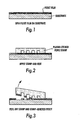
- fig. 1 relates to the lift-up and shows how a PEDOT film is spin deposited on the substrate.
- a plasma etched poly(dimethylsiloxane) stamp is applied to the thin film and simultaneously heated.
- the stamp may be plasma etched to obtain an adhesion between the thin film and the stamp which is stronger than the adhesion between the thin film and the substrate.
- the stamp is lifted and the thin-film polymer in the form of PEDOT adheres to the protruding portion of the stamps, such that the pattern is formed in the thin film PEDOT on the substrate when the stamp is removed.
- a slightly modified PEDOT dispersion is coated onto an elastomeric stamp by spin coating.
- a low molecular weight compound such as ethylene glycol, glycerol or sorbitol in the dispersion
- the surface remains sticky enough to attach to another surface brought close.
- the PEDOT residing on the upper edge of the structure onto a mating surface, at the right temperature and pressure.
- the Put-down method one may be able to transfer films with structures smaller than 100 ⁇ m.
- This method has the added advantage that no limitation to the topology is caused from the filling of channels with liquid, such as in the MIMIC process.
- the surface to be coated does not need to be planar; actually non-even surfaces can be handled.
- Poly(3,4-dioxymethylenethiophene)-polystyrenesulfonate (PEDOT-PSS) (Baytron from Bayer AG) is mixed with glycerol to make a 1:2 weight ratio mixture. The mixture is spin-coated into a thin continuous layer on a glass surface.
- An elastomer stamp formed in poly(dimethylsiloxane) (Sylgard 184, Dow Corning) is plasma-treated for 10 to 30 s in an oxygen plasma. The relief-patterned stamp is brought in conformal contact with the layer, which is then heated to 50-100° C for 15 to 60 s and subsequently removed with the removal of the elastomer stamp.
- glycerol sorbitol could be used, but apparently sorbitol mixed PEDOT-PSS works poorly if at all with Lift-up.
- PEDOT-PSS (Baytron from Bayer AG) is mixed with glycerol to make a 1:1 weight ratio mixture. The mixture is spin-coated into a thin continuous layer on a glass surface.
- An elastomer stamp formed in poly(dimethylsiloxane) (Sylgard 184, Dow Corning) is plasma-treated for 10 to 30 s in an oxygen plasma. The relief-patterned stamp is brought in conformal contact with the layer, which is then heated to 50-100° C for 15 to 60 s and subsequently removed with the removal of the elastomer stamp.
- PEDOT-PSS (Baytron from Bayer AG) is mixed with ethylene glycol to make a 1:1 molar ratio mixture.
- the relief-patterned stamp is dipped into the mixture and dip-coated. It is brought in conformal contact with an ITO surface and part of the layer is deposited from the stamp onto the ITO, leaving a layer of patterned PEDOT-PSS mixture.
- PEDOT-PSS (Baytron from Bayer AG) is mixed with ethylene glycol to make a 1:1 molar ratio mixture.
- the relief-patterned stamp is dip-coated with the mixture. It is brought in conformal contact with an Au surface and part of the layer is deposited from the stamp onto the Au, leaving a layer of patterned PEDOT-PSS mixture.
- PEDOT-PSS (Baytron from Bayer AG) is mixed with glycerol to make a 1:1 molar ratio mixture.
- the relief-patterned stamp is dip-coated with the mixture. It is brought in conformal contact with a Cu surface and part of the layer is deposited from the stamp onto the Cu, leaving a layer of patterned PEDOT-PSS mixture.
- PEDOT-PSS (Baytron from Bayer AG) is mixed with glycerol to make a 1:1 molar ratio mixture.
- the relief-patterned stamp is dip-coated with the mixture. It is brought in conformal contact with a glass surface and part of the layer is deposited from the stamp onto the glass, leaving a layer of patterned PEDOT-PSS mixture.
- PEDOT-PSS (Baytron from Bayer AG) is mixed with glycerol to make a 1:1 molar ratio mixture.
- An elastomer stamp formed in poly(dimethylsiloxane) (Sylgard 184, Dow Corning) is plasma-treated for 10 s in an oxygen plasma.
- the relief-patterned stamp is dip-coated with the mixture. It is brought in conformal contact with an Au surface and part of the layer is deposited from the stamp onto the Au, leaving a layer of patterned PEDOT-PSS mixture.
- the decorated Au surface is exposed to an etchant (gold etch solution: 5g I 2 , 10 g KI dissolved in 250 ml H 2 O) to remove the unprotected Au layer.
Landscapes
- Engineering & Computer Science (AREA)
- Chemical & Material Sciences (AREA)
- Nanotechnology (AREA)
- Physics & Mathematics (AREA)
- General Physics & Mathematics (AREA)
- Manufacturing & Machinery (AREA)
- Crystallography & Structural Chemistry (AREA)
- Condensed Matter Physics & Semiconductors (AREA)
- Mathematical Physics (AREA)
- Theoretical Computer Science (AREA)
- Exposure Of Semiconductors, Excluding Electron Or Ion Beam Exposure (AREA)
- Treatments Of Macromolecular Shaped Articles (AREA)
- Addition Polymer Or Copolymer, Post-Treatments, Or Chemical Modifications (AREA)
- Coating Of Shaped Articles Made Of Macromolecular Substances (AREA)
- Polyethers (AREA)
- Electroluminescent Light Sources (AREA)
- Laminated Bodies (AREA)
- Silicon Polymers (AREA)
- Formation Of Insulating Films (AREA)
- Manufacture Or Reproduction Of Printing Formes (AREA)
- Polyoxymethylene Polymers And Polymers With Carbon-To-Carbon Bonds (AREA)
- Macromolecular Compounds Obtained By Forming Nitrogen-Containing Linkages In General (AREA)
Abstract
Description
- The present invention concerns a method for patterning a polymer film forming a coating on a material surface, wherein the patterning takes place by means of a stamp having a surface with at least one indentation formed therein, and a method for transferring a patterned polymer film onto a material surface by means of a stamp having a surface with at least one indentation formed therein. The invention also concerns the use of methods of this kind.
- The use of conjugated polymers in electronic devices requires means for processing them into patternable thin films. Patterning conducting electrodes and semiconducting polymers in polymer diodes requires patterning of all materials, at a resolution of 0.1-50 µm. This can possibly be accomplished by the use of classical photolithography with help of photoresists, but several new problems arise in the chemical etching of the material and the chemical compatibility with conventional photoresists. It would therefore be desirable to pattern this material with non-photolithographic techniques.
- A new method for patterning is based on elastomeric stamps. Patterning of a surface here requires conformal contact between the stamp and surface. Many variants of these techniques are documented, in particular in the work from G. Whitesides' group at Harvard University (Y. Xia and G. Whitesides, Soft lithography, Angewandte Chemie-International Edition in English 37(5): 551-575 (1998) and Y. Xia and G. Whitesides, Soft lithography, Annual Review of Materials Science, 28:153-184 (1998)).
- The work of Whitesides' group is disclosed in US patent No. 5 512 131, titled "Formation of microstamped patterns on surfaces and derivative articles" (Kumar & Whitesides). This prior art document discloses a method of patterning a material surface, comprising steps of providing a stamp having a surface including at least one indentation formed therein, said indentation configured with a stamping surface defining a first pattern; coating said stamping surface with a molecular species terminating at the first end in a functional group selected to bind to said material; processing said stamping surface in a first orientation and contacting a portion of said material surface with said stamping surface to hold said molecular species against said material surface portion to allow said functional group to bind thereto; and removing said stamping surface to provide a self-assembled molecular species on said material surface according to said first pattern in said first orientation.
- This prior art disclosure amounts to a process wherein a chemical species capable of forming a self-assembled monolayer is coated onto the stamping surface of an elastomeric stamp, said species having a functional group selected to bind to a particular material. The stamping surface is placed against a surface of a material surface and removed to leave a self-assembled monolayer of the species according to the stamping surface pattern of the stamp.
- Further there is known a number of different prior art techniques for patterning surfaces or materials deposited thereon without having to resort to conventional photolithography.
- As a further example of prior art a paper by Zhang, L.G.; Liu, J.F. and Lu, Z.H., titled "Microfabrication on polymer with a contact procedure", Supramolecular Science, Vol. 5, Nos. 5-6:713-715 (Oct-Dec. 1998) discloses the fabrication of thickness-contrast micropatterns based on a contact procedure. Polymer (polydimethylsiloxane) micropost arrays are fabricated with grids as the masters. This contact procedure, which does not rely on etching, extends the present limits of microfabrication. In addition the thickness-contrast micropatterns on the polymer can be replicated to other substrates, such as silicon wafers, with microcontact printing.
- These techniques that are collected in the catchall term soft lithography are based on pattern transfer by a soft rubber stamp in direct contact with the surfaces and materials to be patterned. Soft lithography includes microcontact printing (µCP), replica molding (REM) and micromolding in capillaries (MIMIC). The patterning technique is based on physical contact, not the projection of light through a mask, as in photolithography. The fundamental limits to resolution are due to the range of the van der Waals forces determining the interaction of surfaces (~10 nm), not the diffraction of light in far-field geometries (~0.5 µm).
- An important element of microcontact printing (µCP) is the formation, by selfassembly, of a monomolecular layer of etch resistant organic molecules. Alkanethiols are the preferred species, which chemisorb into molecular thin films on Au, Ag, Cu and other metal surfaces. They form layers of very small thickness (1-3 nm) which are tightly bound (but can be desorbed at high temperatures and by exchange). These alkane layers are used as the resist; a metal layer is protected from etching below the molecular film, and where it is not deposited the metal is removed. The patterning of the resist layer is in its turn done with molecular stamps. A poly(dimethylsiloxane) (PDMS) layer, patterned with protruding and recessed elements in a prior step, is exposed to a solution of alkanethiols; the rubbery stamps are pressed onto a surface for a short time; alkanethiols react with the gold surface when close contact is obtained; and a pattern of protected and non-protected Au is obtained. This layer is now exposed to another alkanethiol, adsorbing from solution onto the unprotected gold surface. A patterned layer is obtained. The process is called microcontact printing (µCP). It has been established that formation of the patterned structure occurs within a few seconds.
- The patterned layer may now be used as ultrathin resists in selective wet etching, or as templates for the control of wetting, dewetting, nucleation and growth or deposition of other materials. Minimal sizes of 35 nm trenches in Au layers have been obtained with etching techniques.
- Patterned self-assembled monolayers (SAMs) allow control of the local hydrophobic/hydrophilic nature of the surface, and therefore act to control the deposition of materials. Water will condense on the hydrophilic part of the surface; this allows us to deposit materials from water solution onto a patterned surface in a regular fashion. Likewise, organic polymers may be deposited onto the hydrophobic surfaces from organic solvents. Both these approaches allow the formation of patterned structures of deposited material. Selective chemical vapour deposition (CVD) processes onto SAMs controlling the nucleation behaviour is another approach for pattern formation in ceramics and metals. Proteins and cells can be selectively adsorbed on patterned surfaces.
- It is easy to pattern non-planar surfaces with this approach, a near impossibility with photolithography. Capillaries of radius of curvature 50 µm have been patterned with structures of dimensions down to a few microns. This enables the construction of more complex structures on patterned and non-planar surfaces, relieving one of the tyranny of planar photolithography.
- The microcontact printing is simple, inexpensive and flexible. With bigger structures (>20 µm) clean room facilities are not necessary. The stamp can be used and reused many times, providing high fidelity reproduction. Because the master structure is normally used as a template to prepare "negatives" (as it were), one can form many identical stamps from a single master, and each one of them can be used some hundred times - multiple copying and parallel processing of the structures is therefore possible. The capital cost of producing the structures is very low. The fabrication of masters of course requires other lithographical techniques, such as photolithography or electron beam lithography, but the multiplication of stamps gives parallel production lines. Micromolding is a small twist to classical molding in that a soft and flexible silicone rubber is used, rather than a hard mold. The elasticity and low surface energy of this mold material allows it to be removed easily from the prepared structure. Replica-molding (REM) can be obtained down to the 30 nm dimensions. Such methods may be used to prepare optical structures as in gratings, microlenses, Fresnel lenses and similar designs for the diffraction and refraction of light. Microprinting is best obtained with the technique named micro-transfer molding (µTM) where a patterned mold is filled with a liquid prepolymer, excess liquid removed and the mold pressed against a surface, irradiated or heated to polymerize. After the liquid precursor is converted into a solid, the mold is peeled away. In a slight modification of this technique (micromolding in capillaries, MIMIC) connected structures are placed in contact with low viscosity liquids, which fill the channels by capillary action. These liquids may carry nanoparticles, or solutions for sol gel conversion, or polymers in solution. After conversion of the liquid to a solid, the mold is removed. Processing of the resulting structure by photochemistry or thermal treatment is now possible, for instance converting a precursor to carbon materials. The remaining structure may now be the functional element - such as an optical waveguide - or a resist to be used to etch the underlying material. In a slight twist to this method, SAMIM (solvent assisted MIMIC), a solvent is used to modify the sample surface to be patterned, and the patterned is defined with a micromold in which the structure is defined.
- The very important aspect of faithful reproduction over large areas and with low defect density is not yet fully resolved. In a recent report from IBM Zurich, it is claimed that structures of 1 micrometer pitch were faithfully replicated without defects over areas of 10 cm2, using µCP or MIMIC.
- Patterning of monolayers of molecules is the most elegant and novel of these prior art methods, but is limited to transfer of monolayers, subsequently used for etch resists and surface activating elements. Transfer of polymer patterns is normally done with MIMIC and microcontact printing. In MIMIC a polymer precursor is patterned by filling channels defined by applying a stamp onto a surface; in microcontact printing a polymer (precursor) fills the channels turned upside down, in such a way as to form the structure which is then transferred to the surface. Transfer of polymer layers to functionally modified surfaces has been reported; see L. Yan, W.T.S. Huck, X.M. Zhao, and G.M. Whitesides, Patterning thin films of poly(ethylene imine) on a reactive SAM using microcontact printing, Langmuir, 15(4): 1208-1214 (1999).
- The patterning of polymers, and in particular conjugated polymers has been reported (see Z. Huang, P.C. Wang, J. Feng, A.G. MacDiarmid, Y. Xia, and G.M. Whitesides, Selective deposition of films of polypyrrole, polyaniline and nickel on hydrophobic/hydrophilic patterned surfaces and applications, Synthetic Metals, 85(1-3):1375-1376 (1997); and Z.Y. Huang, P.C. Wang, A.G. MacDiarmid, Y.N. Xia, and G. Whitesides, Selective deposition of conducting polymers on hydroxyl-terminated surfaces with printed monolayers of alkylsiloxanes as templates, Langmuir 13(24):6480-6484 (1997)) using hydrophobic/hydrophilic modification of monomer adhesion. It may be difficult to deposit high quality polymers from dispersions and solutions with the materials used in these stamps; in particular, the swelling of a poly(dimethylsiloxane) stamp in chloroform prevents the patterning of many of the luminescent polymers used for electroluminescent polymer displays where patterning is desired. These polymers are often solvated in solvents such as chloroform. Likewise, the patterning of water-soluble polymers prohibits the use of some soft lithography techniques, such as MIMIC (Y. Xia and G. Whitesides, Soft lithography, Angewandte Chemie-International Edition in English 37(5): 551-575 (1998) and Y. Xia and G. Whitesides, Soft lithography, Annual Review of Materials Science, 28:153-184 (1998)) as the solvent is required to pass through an elastomeric membrane. Chloroform will swell the stamp, and destroy the fine pattern to be transferred; in the other extreme, water is not easily transported through the extremely non-polar elastomeric stamp, and pattern transfer will be prohibited. Novel patterning methods are therefore desired.
- In regard of certain drawbacks and limitations of the above-mentioned prior art methods, it is thus an object of the present invention to provide methods whereby patterns can be generated in thin films of polymer deposited on material surface by a simple and inexpensive technique based on the use of a specially designed stamp for generating the patterns. Particularly it is another object of the present invention to be able to pattern thin film of polymers which initially form continuous layers and moreover exhibit advantageous electronic or optical properties, e.g. for use as pattern electrodes or pixels in optoelectronic displays.
- Finally, it is also an object of the invention to provide patterned thin films of polymer on a substrate in order to facilitate specific processing of the substrate.
- The above-mentioned objects and advantages are realized with a method for patterning a polymer film according to the invention the method being characterized by depositing onto the material surface a thin film of polymer, applying to the material surface the stamp made of an elastomeric material in conformal contact with the surface of the thin film, such that portions thereof contacting one or more protruding elements of the elastomeric stamp, formed by the at least one indentation thereof, are attached to the protruding element or elements and removed from the material surface with the stamp.
- According to the invention the polymer can advantageously be modified by incorporating additives in order to reduce the cohesive binding of the polymer film, in which case an additive can be a water-soluble organic compound, or selected among ethylene glycol, poly(ethylene glycol), glycerol, sorbitol, polyol, or any combinations thereof.
- According to the invention the polymer can be a water-soluble or dispersed polymer, or a conducting conjugated polymer in its doped or undoped state, or poly(3,4-dioxyethylenethiophene) (PEDOT) or deriving from a copolymer thereof, or one or more mixtures incorporating the monomer (EDOT) form.
- According to the invention it is advantageous modifying the material surface in order to provide a weak adhesion between the material surface and the polymer film to be removed therefrom, and then preferably modifying the material surface by plasma etching.
- According to the invention it is also advantageous modifying the elastomer stamp surface in order to provide a strong adhesion between the stamp and the polymer film to be attached thereto, and then preferably modifying the elastomer stamp surface by plasma etching.
- Finally it is according to the method of the invention advantageous enhancing the adhesion between stamp and polymer film by means of additives to the latter, an additive then preferably being glycerol.
- The above-mentioned object and advantages are also realized according to the present invention with a method for transferring a polymer film, the method being characterized by depositing onto the stamp surface a thin film of polymer, applying the stamp made of an elastomeric material in conformal contact with the material surface, such that the thin film of polymer is transferred thereto from one or more protruding elements of the elastomeric stamp formed by the at least one indentation thereof, and leaving a patterned thin film of polymer on the material surface when removing the stamp therefrom.
- In the above method according to the invention it is advantageous modifying the polymer film by incorporating additives in order to reduce the cohesive binding of the polymer film, the additive then preferably being a water-soluble organic compound, or preferably selected an additive among ethylene glycol, poly(ethylene glycol), glycerol, sorbitol, polyol, or any combinations thereof.
- In the above method according to the invention it is advantageous that the polymer film is a water-soluble or dispersed polymer, or that the polymer is a conducting conjugated polymer in its doped or undoped state, or poly(3,4-dioxyethylenethiophene) (PEDOT) or deriving from a copolymer thereof, or one or more mixtures incorporating the monomer (EDOT).
- In the above method according to the invention it is advantageous modifying the elastomer stamp surface in order to provide a weak adhesion between the elastomer surface and the polymer film to be removed therefrom, and then preferably modifying the elastomer stamp surface by plasma etching.
- In the above method according to the invention it is advantageous modifying the material surface in order to provide a strong adhesion between the material surface and the polymer film to be transferred thereto, and then preferably modifying the material surface by plasma etching.
- Finally the above mentioned objects and advantages are provided with the use of the method for patterning or the method for transferring to provide a patterned etch resist in the form of a thin film of polymer on a gold layer, whereby the gold layer can be removed by etching of the area unprotected by the resist, the polymer preferably being PEDOT.
- Further features and advantages of the method according to the invention are apparent from the appended dependent claims.
- The invention shall now be described in a general manner and in connection with the appended drawing figures in case of one of the methods, as well as with a reference to exemplary embodiments of both the methods.
- In the drawing figures,
- fig. 1 shows the deposition of a thin film of polymer on a substrate,
- fig. 2 the application of a stamp to the thin film polymer, and
- fig. 3 schematically the patterning of the thin film of the polymer.
- A particular polymer of great interest in these devices is the poly(3,4-dioxoethylenethiophene) (PEDOT) which is a commercial polymer from Bayer AG. It is produced in the form of an aqueous dispersion, and can be coated, e.g. spin-coated onto a surface to form a thin film. This film has very attractive properties for polymer electronic devices as it for instance enhances the stability and efficiency of polymer light emitting diodes, or the hole collection in polymer photodiodes, or the hole injection in metal/PEDOT/polymer structures. It is, however, difficult to pattern this polymer dispersion with the hydrophobic polydimethylsiloxane (PDMS) stamp in the MIMIC method. Thus the present invention provides alternative methods of patterning PEDOT films.
- One of the requirements for the use of this patterned film is that sufficient electrical conductivity can be obtained to allow the polymer to be used as the electrode in devices. Surprisingly, the patternable film is obtained with similar additives which has been shown to give enhanced electrical conductivity, up to 80 S/cm, after thermal curing.
- In these methods according to the present invention, a film of modified PEDOT is deposited on the surface to be patterned by spin coating, and patterning is done by removing parts of the film with a suitable elastomer stamp. This is the first method according to the invention and shall subsequently be termed "Lift-up". In the alternative method, a modified PEDOT layer is deposited on the stamp and then transferred onto the surface to be patterned. This is the second method according to the invention and subsequently termed "Put-down".
- These methods are superior to prior art in that they allow patterning of very large areas on (non-planar) surfaces. It is documented in the literature (see Y. Xia and G. Whitesides, Soft lithography, Angewandte Chemie-International Edition in English 37(5): 551-575 (1998); and Y. Xia and G. Whitesides, Soft lithography, Annual Review of Materials Science, 28:153-184 (1998)) that polymers can be deposited onto surfaces in patterns with MIMIC, in which indentations in a stamp act as channels to allow capillary filling with some polymer solution or precursor polymer. This requires that all areas to be filled are connected; an isolated pixel cannot be filled by capillary action. MIMIC will also require long filling time, as the size of channels is reduced and length increased. It is therefore not suited for reel-to-reel production. Both the methods according to the invention are in principle compatible with reel-to-reel production, and also allow the patterning of isolated structures.
- They are also superior in that the patterning of the polymer layer does not (necessarily) require the previous patterning of the surface, as for instance in Z. Huang, P.C. Wang, J. Feng, A.G. MacDiarmid, Y. Xia, and G.M. Whitesides, Selective deposition of films of polypyrrole, polyaniline and nickel on hydrophobic/hydrophilic patterned surfaces and applications, Synthetic Metals, 85(1-3):1375-1376 (1997); and Z.Y. Huang, P.C. Wang, A.G. MacDiarmid, Y.N. Xia, and G. Whitesides, Selective deposition of conducting polymers on hydroxyl-terminated surfaces with printed monolayers of alkylsiloxanes as templates, Langmuir 13(24):6480-6484 (1997), and that polymers, not monomers, are deposited.
- The preparation of the modified polymer is done in order to tune the cohesive energy of the film, which has to allow the rupturing of the film in both methods; it is also done to tune adhesion to the substrate and/or stamp. The internal cohesion of the film is modified by adding low molecular species in the present case, but could in general be any additive giving this function. It is, of course, essential that the additives are in no way detrimental to the function of the layer, and in the present case the additives are actually beneficial to the function.
- When considering the advantages of these methods, we note that Lift-up and Put-down are complementary in the sense that where the former fails, the latter should work. Poor adhesion of the film to be patterned to the substrate suggests that Lift-up should be used; poor adhesion to the stamp suggests that Put-down could be used.
- In Lift-up, the polymer film transfer between stamp and surface is used to pick up parts of a PEDOT film from a substrate, by attaching an elastomeric stamp onto the thin film of PEDOT on a fully covered substrate. The molecular contact between film and stamp breaks up the film, and it can now be micropatterned to any topology by this method. The PEDOT film will also now be prepared with the help of additives, and after transfer the film is cured/converted to a higher conductivity by thermal treatment. Features of dimensions down to 10 µm can easily be patterned. One of the advantages of this technique as compared to MIMIC is that isolated PEDOT pixel can be defined. In this method no solvent is used, which increases the number of materials that can be patterned.
- Specifically fig. 1 relates to the lift-up and shows how a PEDOT film is spin deposited on the substrate. In a second step shown in fig. 2 a plasma etched poly(dimethylsiloxane) stamp is applied to the thin film and simultaneously heated. The stamp may be plasma etched to obtain an adhesion between the thin film and the stamp which is stronger than the adhesion between the thin film and the substrate. In the subsequent and final step in the Lift-up process, shown in fig. 3, the stamp is lifted and the thin-film polymer in the form of PEDOT adheres to the protruding portion of the stamps, such that the pattern is formed in the thin film PEDOT on the substrate when the stamp is removed.
- In Put-down a slightly modified PEDOT dispersion is coated onto an elastomeric stamp by spin coating. By adding a low molecular weight compound such as ethylene glycol, glycerol or sorbitol in the dispersion, the surface remains sticky enough to attach to another surface brought close. For structures with a large enough spacing between the protruding parts this is sufficient to transfer the PEDOT residing on the upper edge of the structure onto a mating surface, at the right temperature and pressure. With the use of the Put-down method one may be able to transfer films with structures smaller than 100 µm. This method has the added advantage that no limitation to the topology is caused from the filling of channels with liquid, such as in the MIMIC process. There is also the advantage that the surface to be coated does not need to be planar; actually non-even surfaces can be handled.
- It shall now be examples of particularly preferred embodiments according to the invention, including both the lift-up and the put-down processes.
- Poly(3,4-dioxymethylenethiophene)-polystyrenesulfonate (PEDOT-PSS) (Baytron from Bayer AG) is mixed with glycerol to make a 1:2 weight ratio mixture. The mixture is spin-coated into a thin continuous layer on a glass surface. An elastomer stamp formed in poly(dimethylsiloxane) (Sylgard 184, Dow Corning) is plasma-treated for 10 to 30 s in an oxygen plasma. The relief-patterned stamp is brought in conformal contact with the layer, which is then heated to 50-100° C for 15 to 60 s and subsequently removed with the removal of the elastomer stamp. - As an alternative to glycerol sorbitol could be used, but apparently sorbitol mixed PEDOT-PSS works poorly if at all with Lift-up.
- PEDOT-PSS (Baytron from Bayer AG) is mixed with glycerol to make a 1:1 weight ratio mixture. The mixture is spin-coated into a thin continuous layer on a glass surface. An elastomer stamp formed in poly(dimethylsiloxane) (Sylgard 184, Dow Corning) is plasma-treated for 10 to 30 s in an oxygen plasma. The relief-patterned stamp is brought in conformal contact with the layer, which is then heated to 50-100° C for 15 to 60 s and subsequently removed with the removal of the elastomer stamp.
- PEDOT-PSS (Baytron from Bayer AG) is mixed with ethylene glycol to make a 1:1 molar ratio mixture. An elastomer stamp formed in poly(dimethylsiloxane) (Sylgard 184, Dow Corning) is plasma-treated for 10 s in an oxygen plasma. The relief-patterned stamp is dipped into the mixture and dip-coated. It is brought in conformal contact with an ITO surface and part of the layer is deposited from the stamp onto the ITO, leaving a layer of patterned PEDOT-PSS mixture.
- PEDOT-PSS (Baytron from Bayer AG) is mixed with ethylene glycol to make a 1:1 molar ratio mixture. An elastomer stamp formed in poly(dimethylsiloxane) (Sylgard 184, Dow Corning) is plasma-treated for 10 s in an oxygen plasma. The relief-patterned stamp is dip-coated with the mixture. It is brought in conformal contact with an Au surface and part of the layer is deposited from the stamp onto the Au, leaving a layer of patterned PEDOT-PSS mixture.
- PEDOT-PSS (Baytron from Bayer AG) is mixed with glycerol to make a 1:1 molar ratio mixture. An elastomer stamp formed in poly(dimethylsiloxane) (Sylgard 184, Dow Corning) is plasma-treated for 10 s in an oxygen plasma. The relief-patterned stamp is dip-coated with the mixture. It is brought in conformal contact with a Cu surface and part of the layer is deposited from the stamp onto the Cu, leaving a layer of patterned PEDOT-PSS mixture.
- PEDOT-PSS (Baytron from Bayer AG) is mixed with glycerol to make a 1:1 molar ratio mixture. An elastomer stamp formed in poly(dimethylsiloxane) (Sylgard 184, Dow Corning) is plasma-treated for 10 s in an oxygen plasma. The relief-patterned stamp is dip-coated with the mixture. It is brought in conformal contact with a glass surface and part of the layer is deposited from the stamp onto the glass, leaving a layer of patterned PEDOT-PSS mixture.
- PEDOT-PSS (Baytron from Bayer AG) is mixed with glycerol to make a 1:1 molar ratio mixture. An elastomer stamp formed in poly(dimethylsiloxane) (Sylgard 184, Dow Corning) is plasma-treated for 10 s in an oxygen plasma. The relief-patterned stamp is dip-coated with the mixture. It is brought in conformal contact with an Au surface and part of the layer is deposited from the stamp onto the Au, leaving a layer of patterned PEDOT-PSS mixture. The decorated Au surface is exposed to an etchant (gold etch solution: 5g I2, 10 g KI dissolved in 250 ml H2O) to remove the unprotected Au layer.
Claims (25)
- A method for patterning a polymer film forming a coating on a material surface, wherein the patterning takes place by means of a stamp having a surface with at least one indentation formed therein, characterized by depositing onto the material surface a thin film of polymer, applying to the material surface the stamp made of an elastomeric material in conformal contact with the surface of the thin film, such that portions thereof contacting one or more protruding elements of the elastomeric stamp formed by the at least one indentation thereof are attached to the protruding element or elements and removed from the material surface with the stamp.
- A method according to claim 1, characterized by modifying the polymer film by incorporating additives in order to reduce the cohesive binding of the polymer film.
- A method according to claim 2, characterized by an additive being a water-soluble organic compound.
- A method according to claim 2, characterized by an additive being selected among ethylene glycol, poly(ethylene glycol), glycerol, sorbitol, polyol, or any combinations thereof.
- A method according to claim 1, characterized by the polymer being a water-soluble or dispersed polymer.
- A method according to claim 1, characterized by the polymer being a conducting conjugated polymer in its doped or undoped state.
- A method according to claim 1, characterized by the polymer being poly(3,4-dioxyethylenethiophene) (PEDOT) or deriving from a copolymer thereof or one or more mixtures incorporating the monomer (EDOT) form.
- A method according to claim 1, characterized by modifying the material surface in order to provide a weak adhesion between the material surface and the polymer film to be removed therefrom.
- A method, according to claim 8, characterized by modifying the material surface by plasma etching.
- A method according to claim 1, characterized by modifying the elastomer stamp surface in order to provide a strong adhesion between the stamp and the polymer film to be attached thereto.
- A method according to claim 10, characterized by modifying the elastomer stamp surface by plasma etching.
- A method according to claim 1, characterized by enhancing the adhesion between stamp and the polymer film by means of additives to the latter.
- A method according to claim 12, characterized by an additive being glycerol.
- A method for transferring a patterned polymer film onto a material surface by means of a stamp having a surface with at least one indentation formed therein, characterized by depositing onto the stamp surface a thin film of polymer, applying the stamp made of an elastomeric material in conformal contact with the material surface, such that the thin film of polymer is transferred thereto from one or more protruding elements of the elastomeric stamp formed by the at least one indentation thereof, and leaving a patterned thin film of polymer on the material surface when removing the stamp therefrom.
- A method according to claim 14, characterized by modifying the polymer film by incorporating additives in order to reduce the cohesive binding of the polymer film.
- A method according to claim 15 , characterized by an additive being a water soluble organic compound.
- A method according to claim 15, characterized by an additive being selected among ethylene glycol, poly(ethylene glycol), glycerol, sorbitol, polyol, or any combinations thereof.
- A method according to claim 14, characterized by the polymer being a water-soluble or dispersed polymer.
- A method according to claim 14, characterized by the polymer being a conducting conjugated polymer in its doped or undoped state.
- A method according to claim 14, characterized by the polymer being poly(3,4-dioxyethylenethiophene) (PEDOT) or deriving from a copolymer thereof or one or more mixtures incorporating the monomer (EDOT).
- A method according to claim 14, characterized by modifying the elastomer stamp surface in order to provide a weak adhesion between the elastomer surface and the polymer film to be removed therefrom.
- A method according to claim 21, characterized by modifying the elastomer stamp surface by plasma etching.
- A method according to claim 14, characterized by modifying the material surface in order to provide a strong adhesion between the material surface and the polymer film to be transferred thereto.
- A method according to claim 23, characterized by modifying the material surface by plasma etching.
- The use of a method according to claims 1 or 14 to provide a patterned etch resist in the form of a thin film of polymer on a gold layer, whereby the gold layer can be removed by etching of the area unprotected by the resist, the polymer preferably being PEDOT.
Applications Claiming Priority (3)
| Application Number | Priority Date | Filing Date | Title |
|---|---|---|---|
| NO992295 | 1999-05-12 | ||
| NO19992295A NO311797B1 (en) | 1999-05-12 | 1999-05-12 | Methods for patterning polymer films and using the methods |
| PCT/NO2000/000157 WO2000070406A1 (en) | 1999-05-12 | 2000-05-12 | Methods for patterning polymer films, and use of the methods |
Publications (2)
| Publication Number | Publication Date |
|---|---|
| EP1192505A1 EP1192505A1 (en) | 2002-04-03 |
| EP1192505B1 true EP1192505B1 (en) | 2006-07-19 |
Family
ID=19903327
Family Applications (1)
| Application Number | Title | Priority Date | Filing Date |
|---|---|---|---|
| EP00927984A Expired - Lifetime EP1192505B1 (en) | 1999-05-12 | 2000-05-12 | Methods for patterning polymer films, and use of the methods |
Country Status (13)
| Country | Link |
|---|---|
| US (1) | US6966997B1 (en) |
| EP (1) | EP1192505B1 (en) |
| JP (1) | JP3469204B2 (en) |
| KR (1) | KR100453255B1 (en) |
| CN (1) | CN100354754C (en) |
| AT (1) | ATE333666T1 (en) |
| AU (1) | AU4628600A (en) |
| DE (1) | DE60029445T2 (en) |
| DK (1) | DK1192505T3 (en) |
| ES (1) | ES2267533T3 (en) |
| NO (1) | NO311797B1 (en) |
| RU (1) | RU2217785C2 (en) |
| WO (1) | WO2000070406A1 (en) |
Cited By (1)
| Publication number | Priority date | Publication date | Assignee | Title |
|---|---|---|---|---|
| CN103030104A (en) * | 2012-12-25 | 2013-04-10 | 江苏大学 | Two-step forming method for producing ultra-oleophobic surface |
Families Citing this family (61)
| Publication number | Priority date | Publication date | Assignee | Title |
|---|---|---|---|---|
| US6663820B2 (en) * | 2001-03-14 | 2003-12-16 | The Procter & Gamble Company | Method of manufacturing microneedle structures using soft lithography and photolithography |
| JP2003089259A (en) * | 2001-09-18 | 2003-03-25 | Hitachi Ltd | Pattern forming method and pattern forming apparatus |
| GB2387268A (en) * | 2002-01-22 | 2003-10-08 | Darren Edward Robertson | Silicon stamped circuits |
| GB0207134D0 (en) | 2002-03-27 | 2002-05-08 | Cambridge Display Tech Ltd | Method of preparation of organic optoelectronic and electronic devices and devices thereby obtained |
| DE10217151A1 (en) * | 2002-04-17 | 2003-10-30 | Clariant Gmbh | Nanoimprint resist |
| EP1516228B1 (en) * | 2002-05-30 | 2009-03-18 | International Business Machines Corporation | Patterning method |
| US7082876B2 (en) * | 2002-06-07 | 2006-08-01 | Obducat Ab | Method for transferring a pattern |
| US8222072B2 (en) * | 2002-12-20 | 2012-07-17 | The Trustees Of Princeton University | Methods of fabricating devices by low pressure cold welding |
| EP1443344A1 (en) * | 2003-01-29 | 2004-08-04 | Heptagon Oy | Manufacturing micro-structured elements |
| US7179396B2 (en) * | 2003-03-25 | 2007-02-20 | Molecular Imprints, Inc. | Positive tone bi-layer imprint lithography method |
| JP3928727B2 (en) * | 2003-09-17 | 2007-06-13 | セイコーエプソン株式会社 | Electrode formation method |
| US7114448B2 (en) * | 2003-11-06 | 2006-10-03 | Palo Alto Research Center, Incorporated | Method for large-area patterning dissolved polymers by making use of an active stamp |
| WO2005060012A1 (en) * | 2003-12-17 | 2005-06-30 | Sumitomo Chemical Company, Limited | Organic light-light conversion device |
| WO2006138272A1 (en) * | 2005-06-13 | 2006-12-28 | Northwestern University | Metal ion-based immobilization |
| KR101264673B1 (en) * | 2005-06-24 | 2013-05-20 | 엘지디스플레이 주식회사 | method for fabricating detail pattern by using soft mold |
| US7572667B2 (en) * | 2006-01-20 | 2009-08-11 | Samsung Electronics Co., Ltd. | Method of forming an organic semiconductor pattern and method of manufacturing an organic thin film transistor using the same |
| TW200739982A (en) * | 2006-04-06 | 2007-10-16 | Nat Univ Chung Cheng | Method for manufacturing full-color organic light-emitting diode array based on microcontact printing technology |
| US20080113283A1 (en) * | 2006-04-28 | 2008-05-15 | Polyset Company, Inc. | Siloxane epoxy polymers for redistribution layer applications |
| KR101309861B1 (en) * | 2006-06-30 | 2013-09-16 | 엘지디스플레이 주식회사 | Printing Device System, Patterning method using the same, and Method for manufacturing Liquid Crystal Display Device using the same |
| US20080110363A1 (en) * | 2006-11-14 | 2008-05-15 | National Chung Cheng University | Physisorption-based microcontact printing process capable of controlling film thickness |
| WO2008091571A2 (en) * | 2007-01-22 | 2008-07-31 | Nano Terra Inc. | High-throughput apparatus for patterning flexible substrates and method of using the same |
| EP2146689B1 (en) | 2007-04-16 | 2020-08-12 | Corium, Inc. | Solvent-cast microneedle arrays containing active |
| JP4432993B2 (en) * | 2007-04-16 | 2010-03-17 | ソニー株式会社 | Pattern forming method and semiconductor device manufacturing method |
| US8911749B2 (en) | 2007-04-16 | 2014-12-16 | Corium International, Inc. | Vaccine delivery via microneedle arrays |
| US20080309900A1 (en) * | 2007-06-12 | 2008-12-18 | Micron Technology, Inc. | Method of making patterning device, patterning device for making patterned structure, and method of making patterned structure |
| US20110039033A1 (en) * | 2008-01-31 | 2011-02-17 | Erika Merschrod | Method of depositing a polymer micropattern on a substrate |
| US8652393B2 (en) * | 2008-10-24 | 2014-02-18 | Molecular Imprints, Inc. | Strain and kinetics control during separation phase of imprint process |
| WO2010061206A1 (en) * | 2008-11-03 | 2010-06-03 | Cambridge Enterprise Limited | Method of patterning an electronic of photonic material |
| JP5195439B2 (en) * | 2009-01-07 | 2013-05-08 | ソニー株式会社 | Printing method and display device manufacturing method |
| GB0912034D0 (en) | 2009-07-10 | 2009-08-19 | Cambridge Entpr Ltd | Patterning |
| GB0913456D0 (en) | 2009-08-03 | 2009-09-16 | Cambridge Entpr Ltd | Printed electronic device |
| WO2011090641A2 (en) * | 2009-12-30 | 2011-07-28 | 3M Innovative Properties Company | Method of using a mask to provide a patterned substrate |
| KR101184161B1 (en) | 2010-04-15 | 2012-09-18 | 한남대학교 산학협력단 | Method for surface modification of patterned Au surface using soft-lithography |
| JP6327852B2 (en) | 2010-05-04 | 2018-05-23 | コリウム インターナショナル, インコーポレイテッド | Methods and devices for transdermal delivery of parathyroid hormone using microprojection arrays |
| TWI378039B (en) * | 2010-06-21 | 2012-12-01 | Compal Electronics Inc | Pattern processing method of a workpiece's surface |
| US8242012B2 (en) | 2010-07-28 | 2012-08-14 | International Business Machines Corporation | Integrated circuit structure incorporating a conductor layer with both top surface and sidewall passivation and a method of forming the integrated circuit structure |
| US9926523B2 (en) | 2010-12-16 | 2018-03-27 | General Electric Company | Cell carriers and methods for culturing cells |
| US9518249B2 (en) | 2010-12-16 | 2016-12-13 | General Electric Company | Cell carrier, associated methods for making cell carrier and culturing cells using the same |
| US9453197B2 (en) | 2010-12-16 | 2016-09-27 | General Electric Company | Methods of making cell carrier |
| US9534206B2 (en) | 2010-12-16 | 2017-01-03 | General Electric Company | Cell carrier, associated methods for making cell carrier and culturing cells using the same |
| US20120156777A1 (en) * | 2010-12-16 | 2012-06-21 | General Electric Company | Cell carrier, associated methods for making cell carrier and culturing cells using the same |
| US9453196B2 (en) | 2010-12-16 | 2016-09-27 | General Electric Company | Cell carrier, methods of making and use |
| KR101218580B1 (en) * | 2011-05-13 | 2013-01-21 | 한국화학연구원 | Method and apparatus for forming graphene pattern by using peeling technique |
| EP2856178B1 (en) | 2012-05-31 | 2020-07-15 | The University of North Carolina at Chapel Hill | Dissolution guided wetting of structured surfaces |
| WO2014021991A1 (en) | 2012-07-31 | 2014-02-06 | New York University | Covalently patterned graphene surfaces by a force accelerated cycloaddition reaction |
| AU2013364053B2 (en) | 2012-12-21 | 2018-08-30 | Corium Pharma Solutions, Inc. | Microarray for delivery of therapeutic agent and methods of use |
| KR101889920B1 (en) | 2012-12-21 | 2018-08-21 | 삼성전자주식회사 | Method of forming a thin film and electronic device and method of manufacturing the same |
| CA2903748C (en) | 2013-03-12 | 2021-11-02 | Corium International, Inc. | Microprojection applicators |
| US9962534B2 (en) | 2013-03-15 | 2018-05-08 | Corium International, Inc. | Microarray for delivery of therapeutic agent, methods of use, and methods of making |
| AU2014237279B2 (en) | 2013-03-15 | 2018-11-22 | Corium Pharma Solutions, Inc. | Microarray with polymer-free microstructures, methods of making, and methods of use |
| BR112015022625B1 (en) | 2013-03-15 | 2023-01-31 | Corium, Inc | MICROSTRUCTURE DEVICE FOR DELIVERY OF THERAPEUTIC AGENT |
| WO2014150285A2 (en) | 2013-03-15 | 2014-09-25 | Corium International, Inc. | Multiple impact microprojection applicators and methods of use |
| WO2016036866A1 (en) | 2014-09-04 | 2016-03-10 | Corium International, Inc. | Microstructure array, methods of making, and methods of use |
| KR101592371B1 (en) * | 2014-12-18 | 2016-02-05 | 광주과학기술원 | Method for transferring highly conductive pedot:pss based electrode |
| US20170342213A1 (en) * | 2014-12-24 | 2017-11-30 | Newsouth Innovations Pty Limited | Electrically conductive polymeric material |
| JP2016203518A (en) * | 2015-04-24 | 2016-12-08 | 株式会社Screenホールディングス | Flat tabular blanket and transcription method with use of blanket |
| US10857093B2 (en) | 2015-06-29 | 2020-12-08 | Corium, Inc. | Microarray for delivery of therapeutic agent, methods of use, and methods of making |
| CN108269656A (en) * | 2016-12-30 | 2018-07-10 | 深圳光启空间技术有限公司 | Meta Materials manufacturing method |
| CN108640081B (en) * | 2018-05-07 | 2019-11-12 | 徐小女 | A kind of preparation method of micro-structure |
| CN109179312B (en) * | 2018-08-03 | 2019-09-24 | 山东科技大学 | A kind of preparation method of pattern metal film |
| CN113211935A (en) * | 2021-05-20 | 2021-08-06 | 汕头市辰安新材料科技有限公司 | Plate making method of mould pressing plate |
Family Cites Families (6)
| Publication number | Priority date | Publication date | Assignee | Title |
|---|---|---|---|---|
| DE3717668A1 (en) * | 1987-05-26 | 1988-12-15 | Hoechst Ag | ELECTRICALLY CONDUCTIVE COATING MEASUREMENT, METHOD FOR THEIR PRODUCTION AND THEIR USE |
| CN1018839B (en) * | 1988-02-13 | 1992-10-28 | 赫稳斯特股份公司 | Use of conductive polymers with improved solubility |
| US5358604A (en) * | 1992-09-29 | 1994-10-25 | Microelectronics And Computer Technology Corp. | Method for producing conductive patterns |
| US5512131A (en) * | 1993-10-04 | 1996-04-30 | President And Fellows Of Harvard College | Formation of microstamped patterns on surfaces and derivative articles |
| RU2082257C1 (en) * | 1995-05-16 | 1997-06-20 | Институт микроэлектроники РАН | Dry lithography process |
| RU2082993C1 (en) * | 1996-05-14 | 1997-06-27 | Коммерческий Банк "Альба Альянс" | Process for manufacturing microrelief on surface of metals (versions) |
-
1999
- 1999-05-12 NO NO19992295A patent/NO311797B1/en unknown
-
2000
- 2000-05-12 AT AT00927984T patent/ATE333666T1/en not_active IP Right Cessation
- 2000-05-12 CN CNB008074518A patent/CN100354754C/en not_active Expired - Fee Related
- 2000-05-12 KR KR10-2001-7014396A patent/KR100453255B1/en not_active Expired - Fee Related
- 2000-05-12 AU AU46286/00A patent/AU4628600A/en not_active Abandoned
- 2000-05-12 US US09/720,259 patent/US6966997B1/en not_active Expired - Fee Related
- 2000-05-12 ES ES00927984T patent/ES2267533T3/en not_active Expired - Lifetime
- 2000-05-12 WO PCT/NO2000/000157 patent/WO2000070406A1/en not_active Ceased
- 2000-05-12 EP EP00927984A patent/EP1192505B1/en not_active Expired - Lifetime
- 2000-05-12 DK DK00927984T patent/DK1192505T3/en active
- 2000-05-12 RU RU2001133272/12A patent/RU2217785C2/en not_active IP Right Cessation
- 2000-05-12 DE DE60029445T patent/DE60029445T2/en not_active Expired - Fee Related
- 2000-05-12 JP JP2000618785A patent/JP3469204B2/en not_active Expired - Fee Related
Cited By (1)
| Publication number | Priority date | Publication date | Assignee | Title |
|---|---|---|---|---|
| CN103030104A (en) * | 2012-12-25 | 2013-04-10 | 江苏大学 | Two-step forming method for producing ultra-oleophobic surface |
Also Published As
| Publication number | Publication date |
|---|---|
| NO311797B1 (en) | 2002-01-28 |
| ATE333666T1 (en) | 2006-08-15 |
| RU2217785C2 (en) | 2003-11-27 |
| DE60029445D1 (en) | 2006-08-31 |
| JP3469204B2 (en) | 2003-11-25 |
| DE60029445T2 (en) | 2007-02-08 |
| CN100354754C (en) | 2007-12-12 |
| ES2267533T3 (en) | 2007-03-16 |
| US6966997B1 (en) | 2005-11-22 |
| CN1350659A (en) | 2002-05-22 |
| WO2000070406A1 (en) | 2000-11-23 |
| JP2002544373A (en) | 2002-12-24 |
| NO992295D0 (en) | 1999-05-12 |
| NO992295L (en) | 2000-11-13 |
| DK1192505T3 (en) | 2006-11-20 |
| KR100453255B1 (en) | 2004-10-15 |
| KR20020026161A (en) | 2002-04-06 |
| EP1192505A1 (en) | 2002-04-03 |
| AU4628600A (en) | 2000-12-05 |
Similar Documents
| Publication | Publication Date | Title |
|---|---|---|
| US6966997B1 (en) | Methods for patterning polymer films, and use of the methods | |
| EP2115794B1 (en) | Deposition of organic layers | |
| US6736985B1 (en) | High-resolution method for patterning a substrate with micro-printing | |
| US6492096B1 (en) | Patterned molecular self-assembly | |
| KR100870250B1 (en) | A method of forming an electronic device, an electronic device formed by the method, a logic circuit including the electronic device, a display and a memory, and a microcutting tool used to form the electronic device. | |
| KR100843552B1 (en) | Nano electrode wire manufacturing method using nano imprint process | |
| US6817293B2 (en) | Patterning method with micro-contact printing and its printed product | |
| US8177991B2 (en) | Method of applying a pattern of metal, metal oxide and/or semiconductor material on a substrate | |
| US20070059497A1 (en) | Reversal imprint technique | |
| US9159925B2 (en) | Process for imprint patterning materials in thin-film devices | |
| CN1633523A (en) | Method for forming a micro-pattern on a substrate by using capillary force | |
| WO1999054786A9 (en) | Elastomeric mask and use in fabrication of devices, inlcuding pixelated electroluminescent displays | |
| CN101517484A (en) | Method to form a pattern of functional material on a substrate | |
| CN102119363A (en) | Template and method of making high aspect ratio template for lithography and use of the template for perforating a substrate at nanoscale | |
| Li et al. | Urethane–acrylate polymers in high-resolution contact printing | |
| KR101107474B1 (en) | Soft Mold and Pattern Method Using the Same | |
| KR101015065B1 (en) | Metal line patterning method on a substrate using nanoimprint lithography | |
| Cheng et al. | A hybrid mask–mould lithography scheme and its application in nanoscale organic thin film transistors | |
| KR20250120800A (en) | METHOD FOR MANUFACTURING CONDUCTIVE polymer FILM WITH NANO-NETWORK STRUCTURE, CONDUCTIVE polymer FILM MANUFACTURED THEREBY, AND BENDING SENSOR COMPRISING THE SAME | |
| Schmidt et al. | Application of Microcontact Printing and Nanoimprint Lithography | |
| KR20070005421A (en) | Contact printing stamp and contact printing method using the same | |
| Li | High-Resolution Contact Transfer via Optimized Polyurethane-Acrylate and Its Application in Fabricating Micro-Patterned Organic Light Emitting Diodes |
Legal Events
| Date | Code | Title | Description |
|---|---|---|---|
| PUAI | Public reference made under article 153(3) epc to a published international application that has entered the european phase |
Free format text: ORIGINAL CODE: 0009012 |
|
| 17P | Request for examination filed |
Effective date: 20011203 |
|
| AK | Designated contracting states |
Kind code of ref document: A1 Designated state(s): AT BE CH CY DE DK ES FI FR GB GR IE IT LI LU MC NL PT SE |
|
| AX | Request for extension of the european patent |
Free format text: AL;LT;LV;MK;RO;SI |
|
| GRAP | Despatch of communication of intention to grant a patent |
Free format text: ORIGINAL CODE: EPIDOSNIGR1 |
|
| GRAS | Grant fee paid |
Free format text: ORIGINAL CODE: EPIDOSNIGR3 |
|
| GRAA | (expected) grant |
Free format text: ORIGINAL CODE: 0009210 |
|
| AK | Designated contracting states |
Kind code of ref document: B1 Designated state(s): AT BE CH CY DE DK ES FI FR GB GR IE IT LI LU MC NL PT SE |
|
| PG25 | Lapsed in a contracting state [announced via postgrant information from national office to epo] |
Ref country code: IT Free format text: LAPSE BECAUSE OF FAILURE TO SUBMIT A TRANSLATION OF THE DESCRIPTION OR TO PAY THE FEE WITHIN THE PRESCRIBED TIME-LIMIT;WARNING: LAPSES OF ITALIAN PATENTS WITH EFFECTIVE DATE BEFORE 2007 MAY HAVE OCCURRED AT ANY TIME BEFORE 2007. THE CORRECT EFFECTIVE DATE MAY BE DIFFERENT FROM THE ONE RECORDED. Effective date: 20060719 Ref country code: AT Free format text: LAPSE BECAUSE OF FAILURE TO SUBMIT A TRANSLATION OF THE DESCRIPTION OR TO PAY THE FEE WITHIN THE PRESCRIBED TIME-LIMIT Effective date: 20060719 |
|
| REG | Reference to a national code |
Ref country code: GB Ref legal event code: FG4D |
|
| REG | Reference to a national code |
Ref country code: CH Ref legal event code: NV Representative=s name: TROESCH SCHEIDEGGER WERNER AG Ref country code: CH Ref legal event code: EP |
|
| REG | Reference to a national code |
Ref country code: IE Ref legal event code: FG4D |
|
| REF | Corresponds to: |
Ref document number: 60029445 Country of ref document: DE Date of ref document: 20060831 Kind code of ref document: P |
|
| REG | Reference to a national code |
Ref country code: SE Ref legal event code: TRGR |
|
| REG | Reference to a national code |
Ref country code: DK Ref legal event code: T3 |
|
| PG25 | Lapsed in a contracting state [announced via postgrant information from national office to epo] |
Ref country code: PT Free format text: LAPSE BECAUSE OF FAILURE TO SUBMIT A TRANSLATION OF THE DESCRIPTION OR TO PAY THE FEE WITHIN THE PRESCRIBED TIME-LIMIT Effective date: 20061219 |
|
| ET | Fr: translation filed | ||
| REG | Reference to a national code |
Ref country code: ES Ref legal event code: FG2A Ref document number: 2267533 Country of ref document: ES Kind code of ref document: T3 |
|
| PGFP | Annual fee paid to national office [announced via postgrant information from national office to epo] |
Ref country code: SE Payment date: 20070502 Year of fee payment: 8 |
|
| PGFP | Annual fee paid to national office [announced via postgrant information from national office to epo] |
Ref country code: FI Payment date: 20070504 Year of fee payment: 8 |
|
| PGFP | Annual fee paid to national office [announced via postgrant information from national office to epo] |
Ref country code: ES Payment date: 20070507 Year of fee payment: 8 |
|
| PGFP | Annual fee paid to national office [announced via postgrant information from national office to epo] |
Ref country code: NL Payment date: 20070524 Year of fee payment: 8 |
|
| PLBE | No opposition filed within time limit |
Free format text: ORIGINAL CODE: 0009261 |
|
| STAA | Information on the status of an ep patent application or granted ep patent |
Free format text: STATUS: NO OPPOSITION FILED WITHIN TIME LIMIT |
|
| PGFP | Annual fee paid to national office [announced via postgrant information from national office to epo] |
Ref country code: CH Payment date: 20070530 Year of fee payment: 8 |
|
| PGFP | Annual fee paid to national office [announced via postgrant information from national office to epo] |
Ref country code: BE Payment date: 20070604 Year of fee payment: 8 |
|
| PGFP | Annual fee paid to national office [announced via postgrant information from national office to epo] |
Ref country code: DK Payment date: 20070621 Year of fee payment: 8 |
|
| 26N | No opposition filed |
Effective date: 20070420 |
|
| PGFP | Annual fee paid to national office [announced via postgrant information from national office to epo] |
Ref country code: IT Payment date: 20070525 Year of fee payment: 8 |
|
| PG25 | Lapsed in a contracting state [announced via postgrant information from national office to epo] |
Ref country code: MC Free format text: LAPSE BECAUSE OF NON-PAYMENT OF DUE FEES Effective date: 20070531 |
|
| PG25 | Lapsed in a contracting state [announced via postgrant information from national office to epo] |
Ref country code: GR Free format text: LAPSE BECAUSE OF FAILURE TO SUBMIT A TRANSLATION OF THE DESCRIPTION OR TO PAY THE FEE WITHIN THE PRESCRIBED TIME-LIMIT Effective date: 20061020 |
|
| PG25 | Lapsed in a contracting state [announced via postgrant information from national office to epo] |
Ref country code: IE Free format text: LAPSE BECAUSE OF NON-PAYMENT OF DUE FEES Effective date: 20070514 |
|
| BERE | Be: lapsed |
Owner name: *THIN FILM ELECTRONICS ASA Effective date: 20080531 |
|
| REG | Reference to a national code |
Ref country code: CH Ref legal event code: PL |
|
| REG | Reference to a national code |
Ref country code: DK Ref legal event code: EBP |
|
| PG25 | Lapsed in a contracting state [announced via postgrant information from national office to epo] |
Ref country code: NL Free format text: LAPSE BECAUSE OF NON-PAYMENT OF DUE FEES Effective date: 20081201 Ref country code: LI Free format text: LAPSE BECAUSE OF NON-PAYMENT OF DUE FEES Effective date: 20080531 Ref country code: CH Free format text: LAPSE BECAUSE OF NON-PAYMENT OF DUE FEES Effective date: 20080531 |
|
| PG25 | Lapsed in a contracting state [announced via postgrant information from national office to epo] |
Ref country code: FI Free format text: LAPSE BECAUSE OF NON-PAYMENT OF DUE FEES Effective date: 20080512 |
|
| PG25 | Lapsed in a contracting state [announced via postgrant information from national office to epo] |
Ref country code: BE Free format text: LAPSE BECAUSE OF NON-PAYMENT OF DUE FEES Effective date: 20080531 |
|
| PG25 | Lapsed in a contracting state [announced via postgrant information from national office to epo] |
Ref country code: DK Free format text: LAPSE BECAUSE OF NON-PAYMENT OF DUE FEES Effective date: 20080531 |
|
| REG | Reference to a national code |
Ref country code: ES Ref legal event code: FD2A Effective date: 20080513 |
|
| PG25 | Lapsed in a contracting state [announced via postgrant information from national office to epo] |
Ref country code: LU Free format text: LAPSE BECAUSE OF NON-PAYMENT OF DUE FEES Effective date: 20070512 Ref country code: IT Free format text: LAPSE BECAUSE OF NON-PAYMENT OF DUE FEES Effective date: 20080512 Ref country code: CY Free format text: LAPSE BECAUSE OF FAILURE TO SUBMIT A TRANSLATION OF THE DESCRIPTION OR TO PAY THE FEE WITHIN THE PRESCRIBED TIME-LIMIT Effective date: 20060719 |
|
| PGFP | Annual fee paid to national office [announced via postgrant information from national office to epo] |
Ref country code: DE Payment date: 20090506 Year of fee payment: 10 Ref country code: FR Payment date: 20090506 Year of fee payment: 10 |
|
| PG25 | Lapsed in a contracting state [announced via postgrant information from national office to epo] |
Ref country code: ES Free format text: LAPSE BECAUSE OF NON-PAYMENT OF DUE FEES Effective date: 20080513 |
|
| PGFP | Annual fee paid to national office [announced via postgrant information from national office to epo] |
Ref country code: GB Payment date: 20090511 Year of fee payment: 10 |
|
| PG25 | Lapsed in a contracting state [announced via postgrant information from national office to epo] |
Ref country code: SE Free format text: LAPSE BECAUSE OF NON-PAYMENT OF DUE FEES Effective date: 20080513 |
|
| GBPC | Gb: european patent ceased through non-payment of renewal fee |
Effective date: 20100512 |
|
| REG | Reference to a national code |
Ref country code: FR Ref legal event code: ST Effective date: 20110131 |
|
| PG25 | Lapsed in a contracting state [announced via postgrant information from national office to epo] |
Ref country code: DE Free format text: LAPSE BECAUSE OF NON-PAYMENT OF DUE FEES Effective date: 20101201 |
|
| PG25 | Lapsed in a contracting state [announced via postgrant information from national office to epo] |
Ref country code: FR Free format text: LAPSE BECAUSE OF NON-PAYMENT OF DUE FEES Effective date: 20100531 |
|
| PG25 | Lapsed in a contracting state [announced via postgrant information from national office to epo] |
Ref country code: GB Free format text: LAPSE BECAUSE OF NON-PAYMENT OF DUE FEES Effective date: 20100512 |