EP1191002A1 - Aluminum nitride sintered compact, ceramic substrate, ceramic heater and electrostatic chuck - Google Patents
Aluminum nitride sintered compact, ceramic substrate, ceramic heater and electrostatic chuck Download PDFInfo
- Publication number
- EP1191002A1 EP1191002A1 EP01906299A EP01906299A EP1191002A1 EP 1191002 A1 EP1191002 A1 EP 1191002A1 EP 01906299 A EP01906299 A EP 01906299A EP 01906299 A EP01906299 A EP 01906299A EP 1191002 A1 EP1191002 A1 EP 1191002A1
- Authority
- EP
- European Patent Office
- Prior art keywords
- ceramic
- ceramic substrate
- fracture
- weight
- conductor
- Prior art date
- Legal status (The legal status is an assumption and is not a legal conclusion. Google has not performed a legal analysis and makes no representation as to the accuracy of the status listed.)
- Withdrawn
Links
Images








Classifications
-
- H—ELECTRICITY
- H05—ELECTRIC TECHNIQUES NOT OTHERWISE PROVIDED FOR
- H05B—ELECTRIC HEATING; ELECTRIC LIGHT SOURCES NOT OTHERWISE PROVIDED FOR; CIRCUIT ARRANGEMENTS FOR ELECTRIC LIGHT SOURCES, IN GENERAL
- H05B3/00—Ohmic-resistance heating
- H05B3/68—Heating arrangements specially adapted for cooking plates or analogous hot-plates
- H05B3/74—Non-metallic plates, e.g. vitroceramic, ceramic or glassceramic hobs, also including power or control circuits
- H05B3/746—Protection, e.g. overheat cutoff, hot plate indicator
-
- B—PERFORMING OPERATIONS; TRANSPORTING
- B32—LAYERED PRODUCTS
- B32B—LAYERED PRODUCTS, i.e. PRODUCTS BUILT-UP OF STRATA OF FLAT OR NON-FLAT, e.g. CELLULAR OR HONEYCOMB, FORM
- B32B18/00—Layered products essentially comprising ceramics, e.g. refractory products
-
- C—CHEMISTRY; METALLURGY
- C04—CEMENTS; CONCRETE; ARTIFICIAL STONE; CERAMICS; REFRACTORIES
- C04B—LIME, MAGNESIA; SLAG; CEMENTS; COMPOSITIONS THEREOF, e.g. MORTARS, CONCRETE OR LIKE BUILDING MATERIALS; ARTIFICIAL STONE; CERAMICS; REFRACTORIES; TREATMENT OF NATURAL STONE
- C04B35/00—Shaped ceramic products characterised by their composition; Ceramics compositions; Processing powders of inorganic compounds preparatory to the manufacturing of ceramic products
- C04B35/01—Shaped ceramic products characterised by their composition; Ceramics compositions; Processing powders of inorganic compounds preparatory to the manufacturing of ceramic products based on oxide ceramics
- C04B35/08—Shaped ceramic products characterised by their composition; Ceramics compositions; Processing powders of inorganic compounds preparatory to the manufacturing of ceramic products based on oxide ceramics based on beryllium oxide
-
- C—CHEMISTRY; METALLURGY
- C04—CEMENTS; CONCRETE; ARTIFICIAL STONE; CERAMICS; REFRACTORIES
- C04B—LIME, MAGNESIA; SLAG; CEMENTS; COMPOSITIONS THEREOF, e.g. MORTARS, CONCRETE OR LIKE BUILDING MATERIALS; ARTIFICIAL STONE; CERAMICS; REFRACTORIES; TREATMENT OF NATURAL STONE
- C04B35/00—Shaped ceramic products characterised by their composition; Ceramics compositions; Processing powders of inorganic compounds preparatory to the manufacturing of ceramic products
- C04B35/01—Shaped ceramic products characterised by their composition; Ceramics compositions; Processing powders of inorganic compounds preparatory to the manufacturing of ceramic products based on oxide ceramics
- C04B35/10—Shaped ceramic products characterised by their composition; Ceramics compositions; Processing powders of inorganic compounds preparatory to the manufacturing of ceramic products based on oxide ceramics based on aluminium oxide
-
- C—CHEMISTRY; METALLURGY
- C04—CEMENTS; CONCRETE; ARTIFICIAL STONE; CERAMICS; REFRACTORIES
- C04B—LIME, MAGNESIA; SLAG; CEMENTS; COMPOSITIONS THEREOF, e.g. MORTARS, CONCRETE OR LIKE BUILDING MATERIALS; ARTIFICIAL STONE; CERAMICS; REFRACTORIES; TREATMENT OF NATURAL STONE
- C04B35/00—Shaped ceramic products characterised by their composition; Ceramics compositions; Processing powders of inorganic compounds preparatory to the manufacturing of ceramic products
- C04B35/01—Shaped ceramic products characterised by their composition; Ceramics compositions; Processing powders of inorganic compounds preparatory to the manufacturing of ceramic products based on oxide ceramics
- C04B35/14—Shaped ceramic products characterised by their composition; Ceramics compositions; Processing powders of inorganic compounds preparatory to the manufacturing of ceramic products based on oxide ceramics based on silica
-
- C—CHEMISTRY; METALLURGY
- C04—CEMENTS; CONCRETE; ARTIFICIAL STONE; CERAMICS; REFRACTORIES
- C04B—LIME, MAGNESIA; SLAG; CEMENTS; COMPOSITIONS THEREOF, e.g. MORTARS, CONCRETE OR LIKE BUILDING MATERIALS; ARTIFICIAL STONE; CERAMICS; REFRACTORIES; TREATMENT OF NATURAL STONE
- C04B35/00—Shaped ceramic products characterised by their composition; Ceramics compositions; Processing powders of inorganic compounds preparatory to the manufacturing of ceramic products
- C04B35/515—Shaped ceramic products characterised by their composition; Ceramics compositions; Processing powders of inorganic compounds preparatory to the manufacturing of ceramic products based on non-oxide ceramics
- C04B35/56—Shaped ceramic products characterised by their composition; Ceramics compositions; Processing powders of inorganic compounds preparatory to the manufacturing of ceramic products based on non-oxide ceramics based on carbides or oxycarbides
- C04B35/5607—Shaped ceramic products characterised by their composition; Ceramics compositions; Processing powders of inorganic compounds preparatory to the manufacturing of ceramic products based on non-oxide ceramics based on carbides or oxycarbides based on refractory metal carbides
-
- C—CHEMISTRY; METALLURGY
- C04—CEMENTS; CONCRETE; ARTIFICIAL STONE; CERAMICS; REFRACTORIES
- C04B—LIME, MAGNESIA; SLAG; CEMENTS; COMPOSITIONS THEREOF, e.g. MORTARS, CONCRETE OR LIKE BUILDING MATERIALS; ARTIFICIAL STONE; CERAMICS; REFRACTORIES; TREATMENT OF NATURAL STONE
- C04B35/00—Shaped ceramic products characterised by their composition; Ceramics compositions; Processing powders of inorganic compounds preparatory to the manufacturing of ceramic products
- C04B35/515—Shaped ceramic products characterised by their composition; Ceramics compositions; Processing powders of inorganic compounds preparatory to the manufacturing of ceramic products based on non-oxide ceramics
- C04B35/56—Shaped ceramic products characterised by their composition; Ceramics compositions; Processing powders of inorganic compounds preparatory to the manufacturing of ceramic products based on non-oxide ceramics based on carbides or oxycarbides
- C04B35/5607—Shaped ceramic products characterised by their composition; Ceramics compositions; Processing powders of inorganic compounds preparatory to the manufacturing of ceramic products based on non-oxide ceramics based on carbides or oxycarbides based on refractory metal carbides
- C04B35/5611—Shaped ceramic products characterised by their composition; Ceramics compositions; Processing powders of inorganic compounds preparatory to the manufacturing of ceramic products based on non-oxide ceramics based on carbides or oxycarbides based on refractory metal carbides based on titanium carbides
-
- C—CHEMISTRY; METALLURGY
- C04—CEMENTS; CONCRETE; ARTIFICIAL STONE; CERAMICS; REFRACTORIES
- C04B—LIME, MAGNESIA; SLAG; CEMENTS; COMPOSITIONS THEREOF, e.g. MORTARS, CONCRETE OR LIKE BUILDING MATERIALS; ARTIFICIAL STONE; CERAMICS; REFRACTORIES; TREATMENT OF NATURAL STONE
- C04B35/00—Shaped ceramic products characterised by their composition; Ceramics compositions; Processing powders of inorganic compounds preparatory to the manufacturing of ceramic products
- C04B35/515—Shaped ceramic products characterised by their composition; Ceramics compositions; Processing powders of inorganic compounds preparatory to the manufacturing of ceramic products based on non-oxide ceramics
- C04B35/56—Shaped ceramic products characterised by their composition; Ceramics compositions; Processing powders of inorganic compounds preparatory to the manufacturing of ceramic products based on non-oxide ceramics based on carbides or oxycarbides
- C04B35/5607—Shaped ceramic products characterised by their composition; Ceramics compositions; Processing powders of inorganic compounds preparatory to the manufacturing of ceramic products based on non-oxide ceramics based on carbides or oxycarbides based on refractory metal carbides
- C04B35/5622—Shaped ceramic products characterised by their composition; Ceramics compositions; Processing powders of inorganic compounds preparatory to the manufacturing of ceramic products based on non-oxide ceramics based on carbides or oxycarbides based on refractory metal carbides based on zirconium or hafnium carbides
-
- C—CHEMISTRY; METALLURGY
- C04—CEMENTS; CONCRETE; ARTIFICIAL STONE; CERAMICS; REFRACTORIES
- C04B—LIME, MAGNESIA; SLAG; CEMENTS; COMPOSITIONS THEREOF, e.g. MORTARS, CONCRETE OR LIKE BUILDING MATERIALS; ARTIFICIAL STONE; CERAMICS; REFRACTORIES; TREATMENT OF NATURAL STONE
- C04B35/00—Shaped ceramic products characterised by their composition; Ceramics compositions; Processing powders of inorganic compounds preparatory to the manufacturing of ceramic products
- C04B35/515—Shaped ceramic products characterised by their composition; Ceramics compositions; Processing powders of inorganic compounds preparatory to the manufacturing of ceramic products based on non-oxide ceramics
- C04B35/56—Shaped ceramic products characterised by their composition; Ceramics compositions; Processing powders of inorganic compounds preparatory to the manufacturing of ceramic products based on non-oxide ceramics based on carbides or oxycarbides
- C04B35/5607—Shaped ceramic products characterised by their composition; Ceramics compositions; Processing powders of inorganic compounds preparatory to the manufacturing of ceramic products based on non-oxide ceramics based on carbides or oxycarbides based on refractory metal carbides
- C04B35/5626—Shaped ceramic products characterised by their composition; Ceramics compositions; Processing powders of inorganic compounds preparatory to the manufacturing of ceramic products based on non-oxide ceramics based on carbides or oxycarbides based on refractory metal carbides based on tungsten carbides
-
- C—CHEMISTRY; METALLURGY
- C04—CEMENTS; CONCRETE; ARTIFICIAL STONE; CERAMICS; REFRACTORIES
- C04B—LIME, MAGNESIA; SLAG; CEMENTS; COMPOSITIONS THEREOF, e.g. MORTARS, CONCRETE OR LIKE BUILDING MATERIALS; ARTIFICIAL STONE; CERAMICS; REFRACTORIES; TREATMENT OF NATURAL STONE
- C04B35/00—Shaped ceramic products characterised by their composition; Ceramics compositions; Processing powders of inorganic compounds preparatory to the manufacturing of ceramic products
- C04B35/515—Shaped ceramic products characterised by their composition; Ceramics compositions; Processing powders of inorganic compounds preparatory to the manufacturing of ceramic products based on non-oxide ceramics
- C04B35/56—Shaped ceramic products characterised by their composition; Ceramics compositions; Processing powders of inorganic compounds preparatory to the manufacturing of ceramic products based on non-oxide ceramics based on carbides or oxycarbides
- C04B35/565—Shaped ceramic products characterised by their composition; Ceramics compositions; Processing powders of inorganic compounds preparatory to the manufacturing of ceramic products based on non-oxide ceramics based on carbides or oxycarbides based on silicon carbide
-
- C—CHEMISTRY; METALLURGY
- C04—CEMENTS; CONCRETE; ARTIFICIAL STONE; CERAMICS; REFRACTORIES
- C04B—LIME, MAGNESIA; SLAG; CEMENTS; COMPOSITIONS THEREOF, e.g. MORTARS, CONCRETE OR LIKE BUILDING MATERIALS; ARTIFICIAL STONE; CERAMICS; REFRACTORIES; TREATMENT OF NATURAL STONE
- C04B35/00—Shaped ceramic products characterised by their composition; Ceramics compositions; Processing powders of inorganic compounds preparatory to the manufacturing of ceramic products
- C04B35/515—Shaped ceramic products characterised by their composition; Ceramics compositions; Processing powders of inorganic compounds preparatory to the manufacturing of ceramic products based on non-oxide ceramics
- C04B35/56—Shaped ceramic products characterised by their composition; Ceramics compositions; Processing powders of inorganic compounds preparatory to the manufacturing of ceramic products based on non-oxide ceramics based on carbides or oxycarbides
- C04B35/565—Shaped ceramic products characterised by their composition; Ceramics compositions; Processing powders of inorganic compounds preparatory to the manufacturing of ceramic products based on non-oxide ceramics based on carbides or oxycarbides based on silicon carbide
- C04B35/575—Shaped ceramic products characterised by their composition; Ceramics compositions; Processing powders of inorganic compounds preparatory to the manufacturing of ceramic products based on non-oxide ceramics based on carbides or oxycarbides based on silicon carbide obtained by pressure sintering
-
- C—CHEMISTRY; METALLURGY
- C04—CEMENTS; CONCRETE; ARTIFICIAL STONE; CERAMICS; REFRACTORIES
- C04B—LIME, MAGNESIA; SLAG; CEMENTS; COMPOSITIONS THEREOF, e.g. MORTARS, CONCRETE OR LIKE BUILDING MATERIALS; ARTIFICIAL STONE; CERAMICS; REFRACTORIES; TREATMENT OF NATURAL STONE
- C04B35/00—Shaped ceramic products characterised by their composition; Ceramics compositions; Processing powders of inorganic compounds preparatory to the manufacturing of ceramic products
- C04B35/515—Shaped ceramic products characterised by their composition; Ceramics compositions; Processing powders of inorganic compounds preparatory to the manufacturing of ceramic products based on non-oxide ceramics
- C04B35/58—Shaped ceramic products characterised by their composition; Ceramics compositions; Processing powders of inorganic compounds preparatory to the manufacturing of ceramic products based on non-oxide ceramics based on borides, nitrides, i.e. nitrides, oxynitrides, carbonitrides or oxycarbonitrides or silicides
- C04B35/58007—Shaped ceramic products characterised by their composition; Ceramics compositions; Processing powders of inorganic compounds preparatory to the manufacturing of ceramic products based on non-oxide ceramics based on borides, nitrides, i.e. nitrides, oxynitrides, carbonitrides or oxycarbonitrides or silicides based on refractory metal nitrides
- C04B35/58014—Shaped ceramic products characterised by their composition; Ceramics compositions; Processing powders of inorganic compounds preparatory to the manufacturing of ceramic products based on non-oxide ceramics based on borides, nitrides, i.e. nitrides, oxynitrides, carbonitrides or oxycarbonitrides or silicides based on refractory metal nitrides based on titanium nitrides, e.g. TiAlON
-
- C—CHEMISTRY; METALLURGY
- C04—CEMENTS; CONCRETE; ARTIFICIAL STONE; CERAMICS; REFRACTORIES
- C04B—LIME, MAGNESIA; SLAG; CEMENTS; COMPOSITIONS THEREOF, e.g. MORTARS, CONCRETE OR LIKE BUILDING MATERIALS; ARTIFICIAL STONE; CERAMICS; REFRACTORIES; TREATMENT OF NATURAL STONE
- C04B35/00—Shaped ceramic products characterised by their composition; Ceramics compositions; Processing powders of inorganic compounds preparatory to the manufacturing of ceramic products
- C04B35/515—Shaped ceramic products characterised by their composition; Ceramics compositions; Processing powders of inorganic compounds preparatory to the manufacturing of ceramic products based on non-oxide ceramics
- C04B35/58—Shaped ceramic products characterised by their composition; Ceramics compositions; Processing powders of inorganic compounds preparatory to the manufacturing of ceramic products based on non-oxide ceramics based on borides, nitrides, i.e. nitrides, oxynitrides, carbonitrides or oxycarbonitrides or silicides
- C04B35/581—Shaped ceramic products characterised by their composition; Ceramics compositions; Processing powders of inorganic compounds preparatory to the manufacturing of ceramic products based on non-oxide ceramics based on borides, nitrides, i.e. nitrides, oxynitrides, carbonitrides or oxycarbonitrides or silicides based on aluminium nitride
-
- C—CHEMISTRY; METALLURGY
- C04—CEMENTS; CONCRETE; ARTIFICIAL STONE; CERAMICS; REFRACTORIES
- C04B—LIME, MAGNESIA; SLAG; CEMENTS; COMPOSITIONS THEREOF, e.g. MORTARS, CONCRETE OR LIKE BUILDING MATERIALS; ARTIFICIAL STONE; CERAMICS; REFRACTORIES; TREATMENT OF NATURAL STONE
- C04B35/00—Shaped ceramic products characterised by their composition; Ceramics compositions; Processing powders of inorganic compounds preparatory to the manufacturing of ceramic products
- C04B35/515—Shaped ceramic products characterised by their composition; Ceramics compositions; Processing powders of inorganic compounds preparatory to the manufacturing of ceramic products based on non-oxide ceramics
- C04B35/58—Shaped ceramic products characterised by their composition; Ceramics compositions; Processing powders of inorganic compounds preparatory to the manufacturing of ceramic products based on non-oxide ceramics based on borides, nitrides, i.e. nitrides, oxynitrides, carbonitrides or oxycarbonitrides or silicides
- C04B35/583—Shaped ceramic products characterised by their composition; Ceramics compositions; Processing powders of inorganic compounds preparatory to the manufacturing of ceramic products based on non-oxide ceramics based on borides, nitrides, i.e. nitrides, oxynitrides, carbonitrides or oxycarbonitrides or silicides based on boron nitride
-
- C—CHEMISTRY; METALLURGY
- C04—CEMENTS; CONCRETE; ARTIFICIAL STONE; CERAMICS; REFRACTORIES
- C04B—LIME, MAGNESIA; SLAG; CEMENTS; COMPOSITIONS THEREOF, e.g. MORTARS, CONCRETE OR LIKE BUILDING MATERIALS; ARTIFICIAL STONE; CERAMICS; REFRACTORIES; TREATMENT OF NATURAL STONE
- C04B35/00—Shaped ceramic products characterised by their composition; Ceramics compositions; Processing powders of inorganic compounds preparatory to the manufacturing of ceramic products
- C04B35/515—Shaped ceramic products characterised by their composition; Ceramics compositions; Processing powders of inorganic compounds preparatory to the manufacturing of ceramic products based on non-oxide ceramics
- C04B35/58—Shaped ceramic products characterised by their composition; Ceramics compositions; Processing powders of inorganic compounds preparatory to the manufacturing of ceramic products based on non-oxide ceramics based on borides, nitrides, i.e. nitrides, oxynitrides, carbonitrides or oxycarbonitrides or silicides
- C04B35/584—Shaped ceramic products characterised by their composition; Ceramics compositions; Processing powders of inorganic compounds preparatory to the manufacturing of ceramic products based on non-oxide ceramics based on borides, nitrides, i.e. nitrides, oxynitrides, carbonitrides or oxycarbonitrides or silicides based on silicon nitride
-
- C—CHEMISTRY; METALLURGY
- C04—CEMENTS; CONCRETE; ARTIFICIAL STONE; CERAMICS; REFRACTORIES
- C04B—LIME, MAGNESIA; SLAG; CEMENTS; COMPOSITIONS THEREOF, e.g. MORTARS, CONCRETE OR LIKE BUILDING MATERIALS; ARTIFICIAL STONE; CERAMICS; REFRACTORIES; TREATMENT OF NATURAL STONE
- C04B35/00—Shaped ceramic products characterised by their composition; Ceramics compositions; Processing powders of inorganic compounds preparatory to the manufacturing of ceramic products
- C04B35/622—Forming processes; Processing powders of inorganic compounds preparatory to the manufacturing of ceramic products
- C04B35/626—Preparing or treating the powders individually or as batches ; preparing or treating macroscopic reinforcing agents for ceramic products, e.g. fibres; mechanical aspects section B
- C04B35/62605—Treating the starting powders individually or as mixtures
- C04B35/62625—Wet mixtures
- C04B35/6264—Mixing media, e.g. organic solvents
-
- C—CHEMISTRY; METALLURGY
- C04—CEMENTS; CONCRETE; ARTIFICIAL STONE; CERAMICS; REFRACTORIES
- C04B—LIME, MAGNESIA; SLAG; CEMENTS; COMPOSITIONS THEREOF, e.g. MORTARS, CONCRETE OR LIKE BUILDING MATERIALS; ARTIFICIAL STONE; CERAMICS; REFRACTORIES; TREATMENT OF NATURAL STONE
- C04B35/00—Shaped ceramic products characterised by their composition; Ceramics compositions; Processing powders of inorganic compounds preparatory to the manufacturing of ceramic products
- C04B35/622—Forming processes; Processing powders of inorganic compounds preparatory to the manufacturing of ceramic products
- C04B35/626—Preparing or treating the powders individually or as batches ; preparing or treating macroscopic reinforcing agents for ceramic products, e.g. fibres; mechanical aspects section B
- C04B35/63—Preparing or treating the powders individually or as batches ; preparing or treating macroscopic reinforcing agents for ceramic products, e.g. fibres; mechanical aspects section B using additives specially adapted for forming the products, e.g.. binder binders
- C04B35/6303—Inorganic additives
-
- H—ELECTRICITY
- H05—ELECTRIC TECHNIQUES NOT OTHERWISE PROVIDED FOR
- H05B—ELECTRIC HEATING; ELECTRIC LIGHT SOURCES NOT OTHERWISE PROVIDED FOR; CIRCUIT ARRANGEMENTS FOR ELECTRIC LIGHT SOURCES, IN GENERAL
- H05B3/00—Ohmic-resistance heating
- H05B3/10—Heating elements characterised by the composition or nature of the materials or by the arrangement of the conductor
- H05B3/12—Heating elements characterised by the composition or nature of the materials or by the arrangement of the conductor characterised by the composition or nature of the conductive material
- H05B3/14—Heating elements characterised by the composition or nature of the materials or by the arrangement of the conductor characterised by the composition or nature of the conductive material the material being non-metallic
- H05B3/141—Conductive ceramics, e.g. metal oxides, metal carbides, barium titanate, ferrites, zirconia, vitrous compounds
- H05B3/143—Conductive ceramics, e.g. metal oxides, metal carbides, barium titanate, ferrites, zirconia, vitrous compounds applied to semiconductors, e.g. wafers heating
-
- H—ELECTRICITY
- H05—ELECTRIC TECHNIQUES NOT OTHERWISE PROVIDED FOR
- H05B—ELECTRIC HEATING; ELECTRIC LIGHT SOURCES NOT OTHERWISE PROVIDED FOR; CIRCUIT ARRANGEMENTS FOR ELECTRIC LIGHT SOURCES, IN GENERAL
- H05B3/00—Ohmic-resistance heating
- H05B3/68—Heating arrangements specially adapted for cooking plates or analogous hot-plates
- H05B3/74—Non-metallic plates, e.g. vitroceramic, ceramic or glassceramic hobs, also including power or control circuits
-
- H—ELECTRICITY
- H10—SEMICONDUCTOR DEVICES; ELECTRIC SOLID-STATE DEVICES NOT OTHERWISE PROVIDED FOR
- H10P—GENERIC PROCESSES OR APPARATUS FOR THE MANUFACTURE OR TREATMENT OF DEVICES COVERED BY CLASS H10
- H10P72/00—Handling or holding of wafers, substrates or devices during manufacture or treatment thereof
- H10P72/04—Apparatus for manufacture or treatment
- H10P72/0431—Apparatus for thermal treatment
- H10P72/0432—Apparatus for thermal treatment mainly by conduction
-
- H—ELECTRICITY
- H10—SEMICONDUCTOR DEVICES; ELECTRIC SOLID-STATE DEVICES NOT OTHERWISE PROVIDED FOR
- H10P—GENERIC PROCESSES OR APPARATUS FOR THE MANUFACTURE OR TREATMENT OF DEVICES COVERED BY CLASS H10
- H10P72/00—Handling or holding of wafers, substrates or devices during manufacture or treatment thereof
- H10P72/04—Apparatus for manufacture or treatment
- H10P72/0431—Apparatus for thermal treatment
- H10P72/0434—Apparatus for thermal treatment mainly by convection
-
- H—ELECTRICITY
- H10—SEMICONDUCTOR DEVICES; ELECTRIC SOLID-STATE DEVICES NOT OTHERWISE PROVIDED FOR
- H10P—GENERIC PROCESSES OR APPARATUS FOR THE MANUFACTURE OR TREATMENT OF DEVICES COVERED BY CLASS H10
- H10P72/00—Handling or holding of wafers, substrates or devices during manufacture or treatment thereof
- H10P72/70—Handling or holding of wafers, substrates or devices during manufacture or treatment thereof for supporting or gripping
- H10P72/72—Handling or holding of wafers, substrates or devices during manufacture or treatment thereof for supporting or gripping using electrostatic chucks
- H10P72/722—Details of electrostatic chucks
-
- H—ELECTRICITY
- H10—SEMICONDUCTOR DEVICES; ELECTRIC SOLID-STATE DEVICES NOT OTHERWISE PROVIDED FOR
- H10P—GENERIC PROCESSES OR APPARATUS FOR THE MANUFACTURE OR TREATMENT OF DEVICES COVERED BY CLASS H10
- H10P72/00—Handling or holding of wafers, substrates or devices during manufacture or treatment thereof
- H10P72/70—Handling or holding of wafers, substrates or devices during manufacture or treatment thereof for supporting or gripping
- H10P72/74—Handling or holding of wafers, substrates or devices during manufacture or treatment thereof for supporting or gripping using temporarily an auxiliary support
-
- B—PERFORMING OPERATIONS; TRANSPORTING
- B32—LAYERED PRODUCTS
- B32B—LAYERED PRODUCTS, i.e. PRODUCTS BUILT-UP OF STRATA OF FLAT OR NON-FLAT, e.g. CELLULAR OR HONEYCOMB, FORM
- B32B38/00—Ancillary operations in connection with laminating processes
- B32B38/04—Punching, slitting or perforating
- B32B2038/042—Punching
-
- B—PERFORMING OPERATIONS; TRANSPORTING
- B32—LAYERED PRODUCTS
- B32B—LAYERED PRODUCTS, i.e. PRODUCTS BUILT-UP OF STRATA OF FLAT OR NON-FLAT, e.g. CELLULAR OR HONEYCOMB, FORM
- B32B2311/00—Metals, their alloys or their compounds
- B32B2311/02—Noble metals
- B32B2311/08—Silver
-
- B—PERFORMING OPERATIONS; TRANSPORTING
- B32—LAYERED PRODUCTS
- B32B—LAYERED PRODUCTS, i.e. PRODUCTS BUILT-UP OF STRATA OF FLAT OR NON-FLAT, e.g. CELLULAR OR HONEYCOMB, FORM
- B32B38/00—Ancillary operations in connection with laminating processes
- B32B38/14—Printing or colouring
- B32B38/145—Printing
-
- C—CHEMISTRY; METALLURGY
- C04—CEMENTS; CONCRETE; ARTIFICIAL STONE; CERAMICS; REFRACTORIES
- C04B—LIME, MAGNESIA; SLAG; CEMENTS; COMPOSITIONS THEREOF, e.g. MORTARS, CONCRETE OR LIKE BUILDING MATERIALS; ARTIFICIAL STONE; CERAMICS; REFRACTORIES; TREATMENT OF NATURAL STONE
- C04B2235/00—Aspects relating to ceramic starting mixtures or sintered ceramic products
- C04B2235/02—Composition of constituents of the starting material or of secondary phases of the final product
- C04B2235/30—Constituents and secondary phases not being of a fibrous nature
- C04B2235/32—Metal oxides, mixed metal oxides, or oxide-forming salts thereof, e.g. carbonates, nitrates, (oxy)hydroxides, chlorides
- C04B2235/3201—Alkali metal oxides or oxide-forming salts thereof
-
- C—CHEMISTRY; METALLURGY
- C04—CEMENTS; CONCRETE; ARTIFICIAL STONE; CERAMICS; REFRACTORIES
- C04B—LIME, MAGNESIA; SLAG; CEMENTS; COMPOSITIONS THEREOF, e.g. MORTARS, CONCRETE OR LIKE BUILDING MATERIALS; ARTIFICIAL STONE; CERAMICS; REFRACTORIES; TREATMENT OF NATURAL STONE
- C04B2235/00—Aspects relating to ceramic starting mixtures or sintered ceramic products
- C04B2235/02—Composition of constituents of the starting material or of secondary phases of the final product
- C04B2235/30—Constituents and secondary phases not being of a fibrous nature
- C04B2235/32—Metal oxides, mixed metal oxides, or oxide-forming salts thereof, e.g. carbonates, nitrates, (oxy)hydroxides, chlorides
- C04B2235/3217—Aluminum oxide or oxide forming salts thereof, e.g. bauxite, alpha-alumina
-
- C—CHEMISTRY; METALLURGY
- C04—CEMENTS; CONCRETE; ARTIFICIAL STONE; CERAMICS; REFRACTORIES
- C04B—LIME, MAGNESIA; SLAG; CEMENTS; COMPOSITIONS THEREOF, e.g. MORTARS, CONCRETE OR LIKE BUILDING MATERIALS; ARTIFICIAL STONE; CERAMICS; REFRACTORIES; TREATMENT OF NATURAL STONE
- C04B2235/00—Aspects relating to ceramic starting mixtures or sintered ceramic products
- C04B2235/02—Composition of constituents of the starting material or of secondary phases of the final product
- C04B2235/30—Constituents and secondary phases not being of a fibrous nature
- C04B2235/32—Metal oxides, mixed metal oxides, or oxide-forming salts thereof, e.g. carbonates, nitrates, (oxy)hydroxides, chlorides
- C04B2235/3224—Rare earth oxide or oxide forming salts thereof, e.g. scandium oxide
- C04B2235/3225—Yttrium oxide or oxide-forming salts thereof
-
- C—CHEMISTRY; METALLURGY
- C04—CEMENTS; CONCRETE; ARTIFICIAL STONE; CERAMICS; REFRACTORIES
- C04B—LIME, MAGNESIA; SLAG; CEMENTS; COMPOSITIONS THEREOF, e.g. MORTARS, CONCRETE OR LIKE BUILDING MATERIALS; ARTIFICIAL STONE; CERAMICS; REFRACTORIES; TREATMENT OF NATURAL STONE
- C04B2235/00—Aspects relating to ceramic starting mixtures or sintered ceramic products
- C04B2235/02—Composition of constituents of the starting material or of secondary phases of the final product
- C04B2235/30—Constituents and secondary phases not being of a fibrous nature
- C04B2235/34—Non-metal oxides, non-metal mixed oxides, or salts thereof that form the non-metal oxides upon heating, e.g. carbonates, nitrates, (oxy)hydroxides, chlorides
- C04B2235/3418—Silicon oxide, silicic acids or oxide forming salts thereof, e.g. silica sol, fused silica, silica fume, cristobalite, quartz or flint
-
- C—CHEMISTRY; METALLURGY
- C04—CEMENTS; CONCRETE; ARTIFICIAL STONE; CERAMICS; REFRACTORIES
- C04B—LIME, MAGNESIA; SLAG; CEMENTS; COMPOSITIONS THEREOF, e.g. MORTARS, CONCRETE OR LIKE BUILDING MATERIALS; ARTIFICIAL STONE; CERAMICS; REFRACTORIES; TREATMENT OF NATURAL STONE
- C04B2235/00—Aspects relating to ceramic starting mixtures or sintered ceramic products
- C04B2235/02—Composition of constituents of the starting material or of secondary phases of the final product
- C04B2235/30—Constituents and secondary phases not being of a fibrous nature
- C04B2235/38—Non-oxide ceramic constituents or additives
- C04B2235/3817—Carbides
- C04B2235/3821—Boron carbides
-
- C—CHEMISTRY; METALLURGY
- C04—CEMENTS; CONCRETE; ARTIFICIAL STONE; CERAMICS; REFRACTORIES
- C04B—LIME, MAGNESIA; SLAG; CEMENTS; COMPOSITIONS THEREOF, e.g. MORTARS, CONCRETE OR LIKE BUILDING MATERIALS; ARTIFICIAL STONE; CERAMICS; REFRACTORIES; TREATMENT OF NATURAL STONE
- C04B2235/00—Aspects relating to ceramic starting mixtures or sintered ceramic products
- C04B2235/02—Composition of constituents of the starting material or of secondary phases of the final product
- C04B2235/30—Constituents and secondary phases not being of a fibrous nature
- C04B2235/38—Non-oxide ceramic constituents or additives
- C04B2235/3852—Nitrides, e.g. oxynitrides, carbonitrides, oxycarbonitrides, lithium nitride, magnesium nitride
- C04B2235/386—Boron nitrides
-
- C—CHEMISTRY; METALLURGY
- C04—CEMENTS; CONCRETE; ARTIFICIAL STONE; CERAMICS; REFRACTORIES
- C04B—LIME, MAGNESIA; SLAG; CEMENTS; COMPOSITIONS THEREOF, e.g. MORTARS, CONCRETE OR LIKE BUILDING MATERIALS; ARTIFICIAL STONE; CERAMICS; REFRACTORIES; TREATMENT OF NATURAL STONE
- C04B2235/00—Aspects relating to ceramic starting mixtures or sintered ceramic products
- C04B2235/02—Composition of constituents of the starting material or of secondary phases of the final product
- C04B2235/30—Constituents and secondary phases not being of a fibrous nature
- C04B2235/38—Non-oxide ceramic constituents or additives
- C04B2235/3852—Nitrides, e.g. oxynitrides, carbonitrides, oxycarbonitrides, lithium nitride, magnesium nitride
- C04B2235/3865—Aluminium nitrides
-
- C—CHEMISTRY; METALLURGY
- C04—CEMENTS; CONCRETE; ARTIFICIAL STONE; CERAMICS; REFRACTORIES
- C04B—LIME, MAGNESIA; SLAG; CEMENTS; COMPOSITIONS THEREOF, e.g. MORTARS, CONCRETE OR LIKE BUILDING MATERIALS; ARTIFICIAL STONE; CERAMICS; REFRACTORIES; TREATMENT OF NATURAL STONE
- C04B2235/00—Aspects relating to ceramic starting mixtures or sintered ceramic products
- C04B2235/02—Composition of constituents of the starting material or of secondary phases of the final product
- C04B2235/30—Constituents and secondary phases not being of a fibrous nature
- C04B2235/38—Non-oxide ceramic constituents or additives
- C04B2235/3852—Nitrides, e.g. oxynitrides, carbonitrides, oxycarbonitrides, lithium nitride, magnesium nitride
- C04B2235/3873—Silicon nitrides, e.g. silicon carbonitride, silicon oxynitride
-
- C—CHEMISTRY; METALLURGY
- C04—CEMENTS; CONCRETE; ARTIFICIAL STONE; CERAMICS; REFRACTORIES
- C04B—LIME, MAGNESIA; SLAG; CEMENTS; COMPOSITIONS THEREOF, e.g. MORTARS, CONCRETE OR LIKE BUILDING MATERIALS; ARTIFICIAL STONE; CERAMICS; REFRACTORIES; TREATMENT OF NATURAL STONE
- C04B2235/00—Aspects relating to ceramic starting mixtures or sintered ceramic products
- C04B2235/02—Composition of constituents of the starting material or of secondary phases of the final product
- C04B2235/30—Constituents and secondary phases not being of a fibrous nature
- C04B2235/42—Non metallic elements added as constituents or additives, e.g. sulfur, phosphor, selenium or tellurium
- C04B2235/422—Carbon
-
- C—CHEMISTRY; METALLURGY
- C04—CEMENTS; CONCRETE; ARTIFICIAL STONE; CERAMICS; REFRACTORIES
- C04B—LIME, MAGNESIA; SLAG; CEMENTS; COMPOSITIONS THEREOF, e.g. MORTARS, CONCRETE OR LIKE BUILDING MATERIALS; ARTIFICIAL STONE; CERAMICS; REFRACTORIES; TREATMENT OF NATURAL STONE
- C04B2235/00—Aspects relating to ceramic starting mixtures or sintered ceramic products
- C04B2235/02—Composition of constituents of the starting material or of secondary phases of the final product
- C04B2235/30—Constituents and secondary phases not being of a fibrous nature
- C04B2235/44—Metal salt constituents or additives chosen for the nature of the anions, e.g. hydrides or acetylacetonate
- C04B2235/446—Sulfides, tellurides or selenides
-
- C—CHEMISTRY; METALLURGY
- C04—CEMENTS; CONCRETE; ARTIFICIAL STONE; CERAMICS; REFRACTORIES
- C04B—LIME, MAGNESIA; SLAG; CEMENTS; COMPOSITIONS THEREOF, e.g. MORTARS, CONCRETE OR LIKE BUILDING MATERIALS; ARTIFICIAL STONE; CERAMICS; REFRACTORIES; TREATMENT OF NATURAL STONE
- C04B2235/00—Aspects relating to ceramic starting mixtures or sintered ceramic products
- C04B2235/02—Composition of constituents of the starting material or of secondary phases of the final product
- C04B2235/50—Constituents or additives of the starting mixture chosen for their shape or used because of their shape or their physical appearance
- C04B2235/54—Particle size related information
- C04B2235/5418—Particle size related information expressed by the size of the particles or aggregates thereof
- C04B2235/5436—Particle size related information expressed by the size of the particles or aggregates thereof micrometer sized, i.e. from 1 to 100 micron
-
- C—CHEMISTRY; METALLURGY
- C04—CEMENTS; CONCRETE; ARTIFICIAL STONE; CERAMICS; REFRACTORIES
- C04B—LIME, MAGNESIA; SLAG; CEMENTS; COMPOSITIONS THEREOF, e.g. MORTARS, CONCRETE OR LIKE BUILDING MATERIALS; ARTIFICIAL STONE; CERAMICS; REFRACTORIES; TREATMENT OF NATURAL STONE
- C04B2235/00—Aspects relating to ceramic starting mixtures or sintered ceramic products
- C04B2235/02—Composition of constituents of the starting material or of secondary phases of the final product
- C04B2235/50—Constituents or additives of the starting mixture chosen for their shape or used because of their shape or their physical appearance
- C04B2235/54—Particle size related information
- C04B2235/5418—Particle size related information expressed by the size of the particles or aggregates thereof
- C04B2235/5445—Particle size related information expressed by the size of the particles or aggregates thereof submicron sized, i.e. from 0,1 to 1 micron
-
- C—CHEMISTRY; METALLURGY
- C04—CEMENTS; CONCRETE; ARTIFICIAL STONE; CERAMICS; REFRACTORIES
- C04B—LIME, MAGNESIA; SLAG; CEMENTS; COMPOSITIONS THEREOF, e.g. MORTARS, CONCRETE OR LIKE BUILDING MATERIALS; ARTIFICIAL STONE; CERAMICS; REFRACTORIES; TREATMENT OF NATURAL STONE
- C04B2235/00—Aspects relating to ceramic starting mixtures or sintered ceramic products
- C04B2235/60—Aspects relating to the preparation, properties or mechanical treatment of green bodies or pre-forms
- C04B2235/602—Making the green bodies or pre-forms by moulding
- C04B2235/6025—Tape casting, e.g. with a doctor blade
-
- C—CHEMISTRY; METALLURGY
- C04—CEMENTS; CONCRETE; ARTIFICIAL STONE; CERAMICS; REFRACTORIES
- C04B—LIME, MAGNESIA; SLAG; CEMENTS; COMPOSITIONS THEREOF, e.g. MORTARS, CONCRETE OR LIKE BUILDING MATERIALS; ARTIFICIAL STONE; CERAMICS; REFRACTORIES; TREATMENT OF NATURAL STONE
- C04B2235/00—Aspects relating to ceramic starting mixtures or sintered ceramic products
- C04B2235/70—Aspects relating to sintered or melt-casted ceramic products
- C04B2235/72—Products characterised by the absence or the low content of specific components, e.g. alkali metal free alumina ceramics
- C04B2235/721—Carbon content
-
- C—CHEMISTRY; METALLURGY
- C04—CEMENTS; CONCRETE; ARTIFICIAL STONE; CERAMICS; REFRACTORIES
- C04B—LIME, MAGNESIA; SLAG; CEMENTS; COMPOSITIONS THEREOF, e.g. MORTARS, CONCRETE OR LIKE BUILDING MATERIALS; ARTIFICIAL STONE; CERAMICS; REFRACTORIES; TREATMENT OF NATURAL STONE
- C04B2235/00—Aspects relating to ceramic starting mixtures or sintered ceramic products
- C04B2235/70—Aspects relating to sintered or melt-casted ceramic products
- C04B2235/72—Products characterised by the absence or the low content of specific components, e.g. alkali metal free alumina ceramics
- C04B2235/723—Oxygen content
-
- C—CHEMISTRY; METALLURGY
- C04—CEMENTS; CONCRETE; ARTIFICIAL STONE; CERAMICS; REFRACTORIES
- C04B—LIME, MAGNESIA; SLAG; CEMENTS; COMPOSITIONS THEREOF, e.g. MORTARS, CONCRETE OR LIKE BUILDING MATERIALS; ARTIFICIAL STONE; CERAMICS; REFRACTORIES; TREATMENT OF NATURAL STONE
- C04B2235/00—Aspects relating to ceramic starting mixtures or sintered ceramic products
- C04B2235/70—Aspects relating to sintered or melt-casted ceramic products
- C04B2235/72—Products characterised by the absence or the low content of specific components, e.g. alkali metal free alumina ceramics
- C04B2235/726—Sulfur content
-
- C—CHEMISTRY; METALLURGY
- C04—CEMENTS; CONCRETE; ARTIFICIAL STONE; CERAMICS; REFRACTORIES
- C04B—LIME, MAGNESIA; SLAG; CEMENTS; COMPOSITIONS THEREOF, e.g. MORTARS, CONCRETE OR LIKE BUILDING MATERIALS; ARTIFICIAL STONE; CERAMICS; REFRACTORIES; TREATMENT OF NATURAL STONE
- C04B2235/00—Aspects relating to ceramic starting mixtures or sintered ceramic products
- C04B2235/70—Aspects relating to sintered or melt-casted ceramic products
- C04B2235/72—Products characterised by the absence or the low content of specific components, e.g. alkali metal free alumina ceramics
- C04B2235/728—Silicon content
-
- C—CHEMISTRY; METALLURGY
- C04—CEMENTS; CONCRETE; ARTIFICIAL STONE; CERAMICS; REFRACTORIES
- C04B—LIME, MAGNESIA; SLAG; CEMENTS; COMPOSITIONS THEREOF, e.g. MORTARS, CONCRETE OR LIKE BUILDING MATERIALS; ARTIFICIAL STONE; CERAMICS; REFRACTORIES; TREATMENT OF NATURAL STONE
- C04B2235/00—Aspects relating to ceramic starting mixtures or sintered ceramic products
- C04B2235/70—Aspects relating to sintered or melt-casted ceramic products
- C04B2235/74—Physical characteristics
- C04B2235/77—Density
-
- C—CHEMISTRY; METALLURGY
- C04—CEMENTS; CONCRETE; ARTIFICIAL STONE; CERAMICS; REFRACTORIES
- C04B—LIME, MAGNESIA; SLAG; CEMENTS; COMPOSITIONS THEREOF, e.g. MORTARS, CONCRETE OR LIKE BUILDING MATERIALS; ARTIFICIAL STONE; CERAMICS; REFRACTORIES; TREATMENT OF NATURAL STONE
- C04B2235/00—Aspects relating to ceramic starting mixtures or sintered ceramic products
- C04B2235/70—Aspects relating to sintered or melt-casted ceramic products
- C04B2235/74—Physical characteristics
- C04B2235/78—Grain sizes and shapes, product microstructures, e.g. acicular grains, equiaxed grains, platelet-structures
- C04B2235/786—Micrometer sized grains, i.e. from 1 to 100 micron
-
- C—CHEMISTRY; METALLURGY
- C04—CEMENTS; CONCRETE; ARTIFICIAL STONE; CERAMICS; REFRACTORIES
- C04B—LIME, MAGNESIA; SLAG; CEMENTS; COMPOSITIONS THEREOF, e.g. MORTARS, CONCRETE OR LIKE BUILDING MATERIALS; ARTIFICIAL STONE; CERAMICS; REFRACTORIES; TREATMENT OF NATURAL STONE
- C04B2235/00—Aspects relating to ceramic starting mixtures or sintered ceramic products
- C04B2235/70—Aspects relating to sintered or melt-casted ceramic products
- C04B2235/96—Properties of ceramic products, e.g. mechanical properties such as strength, toughness, wear resistance
-
- C—CHEMISTRY; METALLURGY
- C04—CEMENTS; CONCRETE; ARTIFICIAL STONE; CERAMICS; REFRACTORIES
- C04B—LIME, MAGNESIA; SLAG; CEMENTS; COMPOSITIONS THEREOF, e.g. MORTARS, CONCRETE OR LIKE BUILDING MATERIALS; ARTIFICIAL STONE; CERAMICS; REFRACTORIES; TREATMENT OF NATURAL STONE
- C04B2235/00—Aspects relating to ceramic starting mixtures or sintered ceramic products
- C04B2235/70—Aspects relating to sintered or melt-casted ceramic products
- C04B2235/96—Properties of ceramic products, e.g. mechanical properties such as strength, toughness, wear resistance
- C04B2235/9607—Thermal properties, e.g. thermal expansion coefficient
-
- C—CHEMISTRY; METALLURGY
- C04—CEMENTS; CONCRETE; ARTIFICIAL STONE; CERAMICS; REFRACTORIES
- C04B—LIME, MAGNESIA; SLAG; CEMENTS; COMPOSITIONS THEREOF, e.g. MORTARS, CONCRETE OR LIKE BUILDING MATERIALS; ARTIFICIAL STONE; CERAMICS; REFRACTORIES; TREATMENT OF NATURAL STONE
- C04B2237/00—Aspects relating to ceramic laminates or to joining of ceramic articles with other articles by heating
- C04B2237/30—Composition of layers of ceramic laminates or of ceramic or metallic articles to be joined by heating, e.g. Si substrates
- C04B2237/40—Metallic
- C04B2237/408—Noble metals, e.g. palladium, platina or silver
-
- C—CHEMISTRY; METALLURGY
- C04—CEMENTS; CONCRETE; ARTIFICIAL STONE; CERAMICS; REFRACTORIES
- C04B—LIME, MAGNESIA; SLAG; CEMENTS; COMPOSITIONS THEREOF, e.g. MORTARS, CONCRETE OR LIKE BUILDING MATERIALS; ARTIFICIAL STONE; CERAMICS; REFRACTORIES; TREATMENT OF NATURAL STONE
- C04B2237/00—Aspects relating to ceramic laminates or to joining of ceramic articles with other articles by heating
- C04B2237/50—Processing aspects relating to ceramic laminates or to the joining of ceramic articles with other articles by heating
-
- C—CHEMISTRY; METALLURGY
- C04—CEMENTS; CONCRETE; ARTIFICIAL STONE; CERAMICS; REFRACTORIES
- C04B—LIME, MAGNESIA; SLAG; CEMENTS; COMPOSITIONS THEREOF, e.g. MORTARS, CONCRETE OR LIKE BUILDING MATERIALS; ARTIFICIAL STONE; CERAMICS; REFRACTORIES; TREATMENT OF NATURAL STONE
- C04B2237/00—Aspects relating to ceramic laminates or to joining of ceramic articles with other articles by heating
- C04B2237/50—Processing aspects relating to ceramic laminates or to the joining of ceramic articles with other articles by heating
- C04B2237/62—Forming laminates or joined articles comprising holes, channels or other types of openings
-
- C—CHEMISTRY; METALLURGY
- C04—CEMENTS; CONCRETE; ARTIFICIAL STONE; CERAMICS; REFRACTORIES
- C04B—LIME, MAGNESIA; SLAG; CEMENTS; COMPOSITIONS THEREOF, e.g. MORTARS, CONCRETE OR LIKE BUILDING MATERIALS; ARTIFICIAL STONE; CERAMICS; REFRACTORIES; TREATMENT OF NATURAL STONE
- C04B2237/00—Aspects relating to ceramic laminates or to joining of ceramic articles with other articles by heating
- C04B2237/50—Processing aspects relating to ceramic laminates or to the joining of ceramic articles with other articles by heating
- C04B2237/70—Forming laminates or joined articles comprising layers of a specific, unusual thickness
- C04B2237/704—Forming laminates or joined articles comprising layers of a specific, unusual thickness of one or more of the ceramic layers or articles
-
- Y—GENERAL TAGGING OF NEW TECHNOLOGICAL DEVELOPMENTS; GENERAL TAGGING OF CROSS-SECTIONAL TECHNOLOGIES SPANNING OVER SEVERAL SECTIONS OF THE IPC; TECHNICAL SUBJECTS COVERED BY FORMER USPC CROSS-REFERENCE ART COLLECTIONS [XRACs] AND DIGESTS
- Y10—TECHNICAL SUBJECTS COVERED BY FORMER USPC
- Y10T—TECHNICAL SUBJECTS COVERED BY FORMER US CLASSIFICATION
- Y10T428/00—Stock material or miscellaneous articles
- Y10T428/25—Web or sheet containing structurally defined element or component and including a second component containing structurally defined particles
-
- Y—GENERAL TAGGING OF NEW TECHNOLOGICAL DEVELOPMENTS; GENERAL TAGGING OF CROSS-SECTIONAL TECHNOLOGIES SPANNING OVER SEVERAL SECTIONS OF THE IPC; TECHNICAL SUBJECTS COVERED BY FORMER USPC CROSS-REFERENCE ART COLLECTIONS [XRACs] AND DIGESTS
- Y10—TECHNICAL SUBJECTS COVERED BY FORMER USPC
- Y10T—TECHNICAL SUBJECTS COVERED BY FORMER US CLASSIFICATION
- Y10T428/00—Stock material or miscellaneous articles
- Y10T428/25—Web or sheet containing structurally defined element or component and including a second component containing structurally defined particles
- Y10T428/252—Glass or ceramic [i.e., fired or glazed clay, cement, etc.] [porcelain, quartz, etc.]
-
- Y—GENERAL TAGGING OF NEW TECHNOLOGICAL DEVELOPMENTS; GENERAL TAGGING OF CROSS-SECTIONAL TECHNOLOGIES SPANNING OVER SEVERAL SECTIONS OF THE IPC; TECHNICAL SUBJECTS COVERED BY FORMER USPC CROSS-REFERENCE ART COLLECTIONS [XRACs] AND DIGESTS
- Y10—TECHNICAL SUBJECTS COVERED BY FORMER USPC
- Y10T—TECHNICAL SUBJECTS COVERED BY FORMER US CLASSIFICATION
- Y10T428/00—Stock material or miscellaneous articles
- Y10T428/26—Web or sheet containing structurally defined element or component, the element or component having a specified physical dimension
-
- Y—GENERAL TAGGING OF NEW TECHNOLOGICAL DEVELOPMENTS; GENERAL TAGGING OF CROSS-SECTIONAL TECHNOLOGIES SPANNING OVER SEVERAL SECTIONS OF THE IPC; TECHNICAL SUBJECTS COVERED BY FORMER USPC CROSS-REFERENCE ART COLLECTIONS [XRACs] AND DIGESTS
- Y10—TECHNICAL SUBJECTS COVERED BY FORMER USPC
- Y10T—TECHNICAL SUBJECTS COVERED BY FORMER US CLASSIFICATION
- Y10T428/00—Stock material or miscellaneous articles
- Y10T428/26—Web or sheet containing structurally defined element or component, the element or component having a specified physical dimension
- Y10T428/263—Coating layer not in excess of 5 mils thick or equivalent
- Y10T428/264—Up to 3 mils
- Y10T428/265—1 mil or less
Definitions
- the present invention relates to an aluminum nitride sintered body which is suitable for a ceramic substrate used in a device for producing/examining a semiconductor such as a hot plate (a ceramic heater), an electrostatic chuck, a wafer prober and the like, as well as to a ceramic substrate produced by forming a conductor inside or on the surface of ceramic of said sintered body and the like, a ceramic heater and an electrostatic chuck using said ceramic substrate.
- a hot plate a ceramic heater
- electrostatic chuck a wafer prober and the like
- a semiconductor producing/examining device including an etching device, a chemical vapor deposition device and the like, a heater, a wafer prober and the like using a metal base material such as stainless steel, aluminum alloy and the like have conventionally been employed.
- the rigidity of the ceramic substrate itself is high. Accordingly, the ceramic heater has an advantage that warping and the like of the substrate can be prevented without making the substrate so thick.
- JP Kokai Hei 11-40330 discloses a heater in which an heating element is provided on the surface of nitride ceramic.
- JP Kokai Hei 9-48669 discloses a heater in which blackened aluminum nitride is used.
- JP Kokai Hei 5-8140 discloses an electrostatic chuck in which nitrides such as aluminum nitride is used.
- JP Kokai Hei 9-48668 discloses carbon-containing aluminum nitride which has the Al-O-N structure.
- the tests performed by the inventors of the present invention have revealed that ceramic particles tend to come off from the main faces and the side surfaces of the abovementioned aluminum nitride sintered body, and thus the generated free particles attach to the semiconductor wafer, in the case of the ceramic substrate in which the aluminum nitride sintered body is used, thereby causing short circuits or disconnection of the circuit and the like formed on the semiconductor wafer. Such short circuits or disconnection and the like may result in malfunction of the semiconductor. Further, as the generated free particles prevent the semiconductor wafer from closely attaching to the ceramic substrate, there is a problem that the semiconductor wafer is heated with an uneven temperature distribution thereof.
- a sintering aid is added to ceramic.
- Such a sintering aid normally exists at the ceramic grain boundary and develops voids therein.
- the sectional view of the fracture exhibits intergranular fracture and thus the ceramic substrate exhibits deteriorated mechanical properties such as deteriorated bending strength at a high temperature.
- the objective of the present invention is to provide an aluminum nitride sintered body, a ceramic substrate, a ceramic heater and an electrostatic chuck, which have excellent mechanical strength and in which coming-off of ceramic particles from the main faces and the side surfaces thereof and generation of free particles are prevented.
- Another object of the present invention is to provide a ceramic substrate for a semiconductor producing/examining device and an electrostatic chuck, in which short circuit is prevented from occurring between conductors provided adjacent to each other in a direction perpendicular and a direction parallel to the substrate main faces inside the ceramic substrate.
- a first aspect of the present invention provides an aluminum nitride sintered body containing sulfur.
- the content of sulfur is preferably in a range of 0.05 to 200 ppm.
- said aluminum nitride sintered body further contains oxygen.
- a second aspect of the present invention provides an aluminum nitride sintered body wherein said aluminum nitride exhibits a state of intragranular fracture at the time of fracture and the average grain diameter of a ceramic grain is 3 ⁇ m or less.
- a third aspect of the present invention provides a ceramic substrate having a conductor formed inside thereof or on the surface thereof , wherein said ceramic substrate has been sintered such that a sectional view of fracture thereof exhibits intragranular fracture.
- the average grain diameter of a ceramic grain is preferably 3 ⁇ m or less.
- said ceramic substrate comprises nitride ceramic and said nitride ceramic contains sulfur therein.
- the content of sulfur is preferably in a range of 0.05 to 200 ppm.
- said ceramic substrate contains oxygen.
- the present invention includes a ceramic heater wherein the ceramic substrate of the third aspect of the present invention is used.
- the present invention further includes an electrostatic chuck wherein the ceramic substrate of the third aspect of the present invention is used.
- a fourth aspect of the present invention provides a ceramic substrate having a conductor inside thereof or on the surface thereof, wherein the average grain diameter of the ceramic grain of the ceramic substrate is preferably 2 ⁇ m or less.
- the present invention includes a ceramic heater wherein the ceramic substrate of the fourth aspect of the present invention is used.
- the present invention further includes an electrostatic chuck wherein the ceramic substrate of the fourth aspect is used.
- a fifth aspect of the present invention provides a ceramic substrate which has a conductor formed inside thereof and is for a semiconductor producing/examining device, wherein: a ceramic layer including said conductor and the vicinity thereof and a ceramic layer located lower than the conductor exhibit a state of intergranular fracture at the time of fracture; and a ceramic layer other than abovementioned layers exhibits a state of intragranular fracture at the time of fracture.
- a sixth aspect of the present invention provides an electrostatic chuck having an electrostatic electrode and a resistance heating element formed inside a ceramic substrate, wherein: a ceramic layer including the electrostatic electrode and the vicinities thereof and a ceramic layer located lower than said electrostatic electrode exhibits a state of intergranular at the time of fracture; and a ceramic layers other than abovementioned ceramic layers exhibit a state of intragranular fracture at the time of fracture.
- the first aspect of the present invention provides an aluminum nitride sintered body containing sulfur.
- the aluminum nitride sintered body according to the first aspect of the present invention contains sulfur. Accordingly, the adhesion property at the ceramic grain boundary is improved. As a result, coming-off of ceramic particles from the main faces or the side surface of the aluminum nitride sintered body can be prevented and thus contamination of the semiconductor wafer by free particles can be avoided.
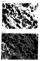
- Fig. 21 is a scanning electron microscope (SEM) photograph which shows a sectional view of fracture of the aluminum nitride sintered body containing sulfur. As shown in Fig. 21, the sectional view of fracture exhibits a state of intragranular fracture (a fracture phenomenon in which fracture occurs inside-grain, which is synonymous with "transgranular fracture”).
- the sectional view of fracture of the aluminum nitride sintered body according to the first aspect of the present invention exhibits the intragranular fracture as shown in Fig. 21. Accordingly, the aluminum nitride sintered body shows no apparent voids and presumably has high bending strength.
- Fig. 23 is a SEM photograph which shows a sectional view of fracture of the conventional aluminum nitride sintered body.
- the sectional view of fracture exhibits a state of "intergranular" fracture (a phenomenon in which fracture occurs at the grain boundary) , in which the binding force by which grains are bound to each other is not so large and thus particles tend to come off and generate free particles when some external or thermal stress is applied on the sintered body or a chemical force acts thereon.
- the problem thus described can be solved.
- the aluminum nitride sintered body of the first aspect of the present invention contains sulfur and oxygen
- sulfur and oxygen serve as catalysts; or sulfur and oxygen are reacted with Al or Si to form a compound which crosslinks between the grains, whereby the ceramic grains are firmly bound to each other.
- coming-off of the particles is prevented and generation of free particles is significantly suppressed.
- the content of sulfur in the aluminum nitride sintered body of the first aspect of the present invention is preferably in a range of 0.05 to 200 ppm (in weight, the same for hereinafter) when measured by what is called the glow discharge-mass spectrum method (the GD-MS method).
- the content of sulfur is less than 0.05 ppm, the effect of binding ceramic grains may not be obtained in a satisfactory manner.
- the content of sulfur exceeds 200 ppm, the sintering property deteriorates and the binding of ceramic grains may be poor.
- the range of the sulfur content which is suitable for demonstrating the effect of the first aspect of the present invention is 0.05 to 200 ppm.
- the sulfur content is particularly suitable when it is in a range of 0.1 to 100 ppm because, when the sulfur content is within this range, the sintering of aluminum nitride is not hindered and the sectional state of fracture of the ceramic can be adjusted to be the intragranular fracture.
- Sulfur may exist in the form of a sulfur atom, a sulfur ion or a sulfur compound in the sintered body. Accordingly, such a sulfur compound may be added to the raw material powder when the sintered body is produced.
- the sulfur compound examples include a thermoplastic resin such as polyether sulfone (PES), polyphenylene sulfide (PPS), polysulfone (PSF) and the like, an inorganic compound such as calcium sulfate, sodium sulfate, zinc sulfide, iron sulfide, calcium sulfide (CaS) and the like.
- a thermoplastic resin such as polyether sulfone (PES), polyphenylene sulfide (PPS), polysulfone (PSF) and the like
- an inorganic compound such as calcium sulfate, sodium sulfate, zinc sulfide, iron sulfide, calcium sulfide (CaS) and the like.
- the aluminum nitride sintered body contains oxygen.
- the content of oxygen is preferably in a range of 0.1 to 10 weight %.
- the content of oxygen is less than 0.1 weight %, the sintering property deteriorates and voids are more likely to be generated at the grain boundary, whereby the bending strength of the aluminum nitride sintered body at a high temperature may be lowered.
- the content of oxygen exceeds 10 weight %, the oxygen itself may become the void and drop the strength at a high temperature.
- the content of oxygen described above is adjusted by heating the raw material powder in the air or oxygen or adding an oxide-type sintering aid.
- an alkali metal oxide, an alkali earth metal oxide, a rare earth oxide may be used.
- CaO, Na 2 O, Li 2 O, Rb 2 O and Y 2 O 3 are preferable.
- Alumina and/or silica may further be used.
- the content of the sintering aid is preferably in a range of 0.1 to 20 weight %.
- the amount thereof to be added is preferably 1.0 parts by weight or less and more preferably 0.3 parts by weight or less with respect to 100 parts by weight of the ceramic raw material.
- the porosity of the aluminum nitride sintered body is preferably 0, or no more than 5 %. This is because, when the porosity exceeds 5 %, the heat conductivity may be lowered or warp may be generated at a high temperature.
- the breakdown voltage at a high temperature becomes especially high.
- the fracture toughness value thereof becomes high. Accordingly, regarding which structure is to be selected, the choice should be made in consideration of the required property.
- the abovementioned porosity is preferably measured by the Archimedes' method. This method includes the steps of: pulverizing the sintered body to obtain the specific gravity thereof; and calculating the porosity from the obtained true specific gravity and the apparent specific gravity.
- the pore diameter of the maximum pore is preferably 50 ⁇ m or less.
- the pore diameter of the maximum pore is preferably 10 ⁇ m or less, because the degree of warp at a temperature of 200 °C or higher is reduced when the pore diameter is in this range.
- the porosity or the pore diameter of the maximum pore is adjusted by changing the pressurizing duration, the applied pressure, the temperature during the sintering process or an additive such as SiC, BN and the like .
- SiC or BN serves to generate pores because these compounds inhibit sintering.
- the measurement of the pore diameter of the maximum pore is performed by: preparing five samples and mirror-grinding the surface thereof; photographing the surface of each sample at ten sites by an electron microscope at the magnification rate of 2000 times to 5000 times; selecting the maximum pore diameter from each photograph; and regarding the average of the maximum pore diameter of the 50 shots as the pore diameter of the maximum pore.
- Young's modulus in a temperature range of 25 to 800 °C is preferably 280 Gpa or more.
- Young's modulus is smaller than 280 GPa, the rigidity is so low that, when the aluminum nitride sintered body is shaped to a plate-shaped body, the degree of warp at the time of heating is hard to be reduced.
- the aluminum nitride sintered body preferably contains carbon in an amount of 50 to 5000 ppm.
- the aluminum nitride sintered body can be blackened so that the radiation heat can be fully utilized when the aluminum nitride sintered body is used as a ceramic heater.
- the carbon may be amorphous or crystalline.
- amorphous carbon When amorphous carbon is used, the drop in the volume resistivity at a high temperature can be prevented.
- the crystalline carbon is used, the drop in the heat conductivity at a high temperature can be prevented. Accordingly, both crystalline carbon and amorphous carbon may be used together depending on the purpose.
- the content of carbon is preferably in a range of 200 to 2000 ppm.
- the amorphous carbon can be obtained by firing a hydrocarbon composed only of C, H and O, preferably a saccharide, in the air.
- a hydrocarbon composed only of C, H and O, preferably a saccharide
- As the crystalline carbon graphite powder and the like can be used.
- carbon can be obtained by heat-decomposing an acrylic resin in an inactive atmosphere and thereafter heating and pressurizing the product.
- the degree of crystallinity or amorphousness can be adjusted by changing the acid value of the acrylic resin.
- the aluminum nitride sintered body of the first aspect of the present invention contains carbon therein, it is preferable that carbon is added so that the brightness of the aluminum nitride sintered body is N6 or less when evaluated as the value according to the definition of JIS Z 8721.
- the aluminum nitride sintered body having such brightness exhibits excellent heat radiation and excellently conceals the conductors and the like embedded therein.
- the brightness N is defined as follows: the brightness of ideal black is made to 0; that of ideal white is made to 10; respective colors are divided into 10 parts in the manner that the brightness of the respective colors is recognized stepwise between the brightness of black and that of white at equal intensity intervals; and the resultant parts are indicated by symbols N0 to N10, respectively.
- a second aspect of the present invention provides an aluminum nitride sintered body which exhibits a state of intragranular fracture at the time of fracture and the average grain diameter of the ceramic grain is 3 ⁇ m or less.
- the aluminum nitride sintered body of the second aspect of the present invention exhibits intragranular fracture at the sectional view of fracture thereof and is controlled so as to have the average grain diameter of the ceramic grain of 3 ⁇ m or less. Accordingly, in the aluminum nitride sintered body, coming-off of the particles is hardly observed and thus free particles are less likely to be generated on the silicon wafer and the like . Further, as there hardly exist any barriers between grains of the aluminum nitride sintered body, the strength of the sintered body at a high temperature becomes high.
- the sectional view of fracture of the aluminum nitride sintered body of the second aspect of the present invention is intragranular fracture or not.
- the intragranular fracture of the second aspect of the present invention represents, similarly to the first aspect of the present invention, the case in which fracture occurs inside ceramic grains and not at the boundary between ceramic grains when the sectional view of fracture is observed, and is synonymous with the term "transgranular fracture".
- the average grain diameter is obtained by: mirror-grinding the sintered body; thereafter measuring the length of the longer axis of a grain constituting the sintered body at arbitrary ten sites; and calculating the average of the ten lengths as the average grain diameter.
- the average particle diameter of ceramic powder used when the aluminum nitride sintered body of the second aspect of the present invention is produced is preferably in a range of 0.2 to 1.5 ⁇ m.
- the average particle diameter is smaller than 0.2 ⁇ m, the bulk density of the ceramic formed body drops too low to effect sintering poorly or abnormal grain growth may be observed.
- the average particle diameter exceeds 1.5 ⁇ m, the grain diameter of the obtained sintered body exceeds 3 ⁇ m.
- a sintering aid such as an alkali metal oxide, an alkali earth metal oxide, a rare earth oxide and the like is generally added.
- the amount of the sintering aid to be added is preferably 1.0 parts by weight or less and more preferably 0.3 parts by weight or less with respect to 100 parts by weight of the ceramic raw material.
- the amount of the sintering aid to be added exceeds 1.0 parts by weight, the aluminum nitride sintered body obtained by sintering may exhibit a state of intergranular fracture, whereby the strength such as the bending strength at a high temperature of the produced aluminum nitride sintered body may be lowered.
- the sintering aid include CaO, Y 2 O 3 , Na 2 O, Li 2 O, Rb 2 O and the like.
- the aluminum nitride sintered body of the second aspect of the present invention exhibits a state of intragranular fracture at the time of fracture and the average grain diameter of the ceramic grain thereof is 3 ⁇ m or less.
- the method of producing such an aluminum nitride sintered body is not particularly restricted, and the aluminum nitride sintered body can be produced by maintaining the firing temperature within a range of 1700 to 1800 °C during the firing process, after adding the sintering aid in the condition as described above.
- the firing temperature is below 1700 °C, the sintering of ceramic particles may not proceed in a sufficient manner.
- the firing temperature exceeds 1800 °C, the average grain diameter of the crystal grains constituting the aluminum nitride sintered body exceeds 3 ⁇ m and the sectional view of fracture may exhibit the intergranular fracture when the sintered body is fractured.
- the grain growth of the ceramic powder during the firing process can be suppressed and thus the average grain diameter of grains constituting the obtained aluminum nitride sintered body can be suppressed to 3 ⁇ m or less.
- the aluminum nitride sintered body obtained by carrying out firing in the abovementioned condition preferably contains oxygen in an amount of 0.05 to 10 weight %.
- oxygen is less than 0.05 weight %, the sintering does not proceed and fracture occurs at the grain boundary, whereby voids are generated in the sintered body and the bending strength thereof at a high temperature drops.
- oxygen and the like locally deposited at the grain boundary become voids, whereby the bending strength of the sintered body at a high temperature drops.
- the sintering aid which has been added when the formed body containing the raw material powder is produced, hardly remains in the sintered body.
- Y 2 O 3 is added to 100 parts by weight of the ceramic raw material when the aluminum nitride sintered body is produced, Y 2 O 3 is dispersed from the surface of the sintered body during the sintering process and scattered out from the surface, whereby Y 2 O 3 hardly remains in the resulting sintered body.
- the grains constituting the aluminumnitride sintered body are firmly bound to each other. Accordingly, if a large force is applied on the aluminum nitride sintered body, fracture does not occur at the grain boundary but proceeds only at the crystal face at which the binding force between atoms in the grain is relatively weak.
- the aluminum nitride sintered body of the second aspect of the present invention contains oxygen and, similarly to the first aspect of the present invention, has no pore, or if the aluminum nitride sintered body has any pore, it is preferable that the porosity is 5 % or less and the pore diameter of the maximum pore is 50 ⁇ m or less. Further, it is preferable that the pore diameter of the maximum pore is 10 ⁇ m or less.
- the content of carbon in the aluminum nitride sintered body and the brightness of the aluminum nitride sintered body according to the second aspect of the present invention are substantially the same as those of the first aspect of the present invention, and thus description thereof will be omitted.
- the aluminum nitride sintered body of the first and second aspects of the present invention can be used for a ceramic substrate, a ceramic heater and an electrostatic chuck of the present invention described below, and is particularly suitable for a ceramic substrate, a ceramic heater and an electrostatic chuck employed for a semiconductor producing/examining device.
- a third aspect of the present invention provides a ceramic substrate having a conductor formed inside thereof or on the surface thereof, wherein said ceramic substrate has been sintered such that a sectional view of fracture thereof exhibits intragranular fracture.
- the ceramic substrate of the third aspect of the present invention has been sintered such that a sectional view of fracture thereof exhibits intragranular fracture, the ceramic substrate produces little coming-off of particles and thus free particles are less likely to be generated, Further, as the ceramic substrate has little barriers between the grains thereof, the strength thereof at a high temperature becomes high.
- the ceramic which exhibits intragranular fracture at the time of fracture has high rigidity and does not warp, whereby the ceramic is less likely to warp by its own weight even at a high temperature.
- the substrate is likely to warp due to its own weight at a high temperature.
- a clearance is generated between the ceramic substrate and the semiconductor wafer or the distance between the ceramic substrate and the semiconductor wafer becomes uneven, thereby causing a problem that the semiconductor wafer cannot be heated evenly or the semiconductor wafer tends to be broken when a stress is applied thereon.
- the degree of warp is small (100 ⁇ m or less) not only at the room temperature but also at a high temperature, the problem of heating property with evenness of a semiconductor wafer; or the problem that the semiconductor wafer tends to be broken when it is used for a wafer prober, can be solved.
- the ceramic substrate of the present invention is preferably used in a temperature range of 100 to 800 °C, because the ceramic substrate of the present invention especially suppresses warp and improves strength thereof at a high temperature.
- the ceramic substrate of the present invention is most preferably used at a temperature of 200 °C or higher.
- a sintered body which has excellent adhesion property at the boundary of ceramic grains is formed by, for example: preparing a formed body with adding sulfur to the ceramic powder and then firing the formed body; or firstly oxidizing the surface of particles of the nitride ceramic raw material, adding an oxide thereto and then subjecting the mixture to forming and firing.
- a sintered body formed in such a manner is fractured, a sectional view of fracture thereof exhibits the intragranular fracture.
- the adhesion property at the boundary of the ceramic grain is improved by adding sulfur before sintering, probably because sulfur facilitates the liquid phase sintering reaction of the nitride ceramic or because sulfur is reacted with oxygen or an element constituting ceramic (for instance, Al in the case of aluminum nitride, Si in the case of silicon nitride) , similarly to the first aspect of the present invention.
- the average grain diameter of ceramic grains constituting the ceramic substrate of the third aspect of the present invention is preferably 3 ⁇ m or less.
- the average grain diameter of the ceramic grains is in this range, the strength of the ceramic substrate can become further high and contamination of the silicone wafer and the like by free particles can be prevented.
- the average grain diameter is obtained by: mirror-grinding the sintered body; thereafter measuring the length of the longer axis of a grain constituting the sintered body at arbitrary ten sites; and calculating the average of the ten lengths as the average grain diameter, similarly to the aluminum nitride sintered body of the second aspect of the present invention.
- the ceramic substrate of the third aspect of the present invention comprises nitride ceramic which preferably contains sulfur therein.
- the sulfur content in the abovementioned nitride ceramic is preferably 0.05 to 200 ppm and more preferably 0.1 to 100 ppm, similarly to the first aspect of the present invention.
- Sulfur may exist in the form of a sulfur atom, a sulfur ion or a sulfur compound in the nitride ceramic. Accordingly, such a sulfur compound may be added to the raw material powder when the ceramic substrate is produced.
- sulfur compound examples include those listed in the first aspect of the present invention and the like.
- the ceramic substrate of the third aspect of the present invention preferably contains oxygen .
- the content of oxygen is preferably in a range of 0.05 to 10 weight % and more preferably in a range of 0.1 to 10 weight %.
- the content of oxygen is less than 0.05 weight %, the sintering does not proceed and fracture occurs at the grain boundary, also voids are generated in the ceramic substrate thus the bending strength thereof at a high temperature drops.
- oxygen and the like locally deposited at the grain boundary become voids, whereby the bending strength of the nitride ceramic at a high temperature drops.
- the content of oxygen is adjusted by: heating the raw material powder in the air or oxygen; or adding an oxide-type sintering aid.
- the sintering aid include those listed as the sintering aid for the aluminum nitride sintered body of the present invention.
- the ceramic substrate of the third aspect of the present invention contains sulfur and oxygen
- sulfur and oxygen serve as catalysts; or sulfur and oxygen are reacted with Al or Si to form a compound which crosslinks between the grains, whereby the ceramic grains are firmly bound to each other, as described in the first aspect of the present invention.
- coming-off of the particles is presumably prevented and generation of free particles is significantly suppressed.
- the ceramic substrate of the third aspect of the present invention may comprise a sintered body obtained by: first oxidizing the surface of particles of the nitride ceramic raw material; adding oxides thereto; and then subjecting the mixture to forming and firing.
- the oxide to be added is preferably the oxide of the element which constitutes the nitride ceramic, because such an oxide is substantially the same as the surface oxide layer of the nitride ceramic and very significantly facilitates the sintering process.
- the surface of the nitride ceramic is heated in oxygen or the air at a temperature of 500 to 1000 °C for 10 minutes to 3 hours.
- the sintered body obtained by adding the abovementioned oxide to the raw material powder and subjecting the mixture to forming and sintering contains Si and/or S.
- the content of Si is preferably in a range of 0.05 to 50 ppm and the content of S is preferably in a range of 0.05 to 80 ppm. (each by weight) Si and S presumably serve to bind the oxidized layer of the nitride ceramic surface to the added oxide .
- the ceramic substrate of the third aspect of the present invention by subjecting the ceramic substrate to fracture and then observing the sectional view of the fracture of an electron microscope photograph taken at a magnification of 2000 to 5000 times, it can be confirmed whether the sectional view of fracture of the ceramic substrate exhibits intragranular fracture or not, similarly to the case of the aluminum nitride of the present invention.
- the porosity of the ceramic substrate is preferably in a range of 0, or no more than 5 %, similarly to the case of the aluminum nitride sintered body of the present invention.
- the heat conductivity may drop or warp may be generated at a high temperature.
- the breakdown voltage at a high temperature becomes especially high.
- the fracture toughness value thereof becomes high. Accordingly, regarding which structure is to be selected, the choice should be made in consideration of the required property.
- the pore diameter of the maximum pore is preferably 50 ⁇ m or less.
- the pore diameter of the maximum pore exceeds 50 ⁇ m, high breakdown voltage property may not be reliably obtained at a high temperature, at a temperature at 200 °C or higher, in particular.
- the pore diameter of the maximum pore is preferably 10 ⁇ m or less, because the degree of warp at a temperature of 200 °C or higher is reduced when the porosity is in this range.
- the porosity or the pore diameter of the maximum pore is adjusted by changing the pressurizing duration, the applied pressure, the temperature during the sintering process or additive such as SiC, BN and the like.
- SiC or BN serves to generate pores because these compounds inhibit sintering.
- the measurement of the pore diameter of the maximum pore and the measurement of the porosity are performed by the methods similar to those employed in the measurement of the pore diameter of the maximum pore or the measurement of the porosity of the aluminum nitride sintered body of the present invention.
- the Young's modulus in a temperature range of 25 to 800 °C of the ceramic substrate of the third aspect of the present invention is preferably 280 Gpa or more, similarly to the case of the aluminum nitride sintered body of the first aspect of the present invention.
- the ceramic substrate preferably contains carbon in an amount of 50 to 5000 ppm and more preferably in an amount of 200 to 2000 ppm, similarly to the case of the abovementioned aluminum nitride sintered body.
- the carbon may be amorphous or crystalline, similarly to the abovementioned aluminum nitride sintered body.
- the ceramic substrate of the third aspect of the present invention contains carbon therein, it is preferable that carbon is added so that the brightness of the ceramic substrate is N6 or lower when evaluated as the value according to the definition of JIS Z 8721.
- the ceramic substrate having such brightness exhibits excellent heat radiation and excellently conceals the conductors and the like embedded therein.
- the ceramic substrate of the third aspect of the present invention preferably contains oxides.
- the oxide include alumina (Al 2 O 3 ), rubidium oxide (Rb 2 O), lithium oxide (Li 2 O), calcium oxide (CaO), silica (SiO 2 ) and the like.
- the content of the oxide is preferably in a range of 0.1 to 20 weight %.
- alumina is especially preferable as the oxide.
- silica is especially preferable as the oxide.
- the amount thereof to be added is preferably 1.0 parts by weight or less and more preferably 0.3 parts by weight or less with respect to 100 parts by weight of the ceramic material.
- a ceramic heater and an electrostatic chuck using the abovementioned ceramic substrate of the third aspect of the present invention is also included in the present invention.
- the ceramic heater and the electrostatic chuck of the third aspect of the present invention have been sintered such that the sectional view of fracture thereof exhibits intragranular fracture, similarly to the case of the ceramic substrate of the third aspect of the present invention. Accordingly, particles are less likely to come off in the ceramic heater and the electrostatic chuck and thus free particles are less likely to be generated. Further, as there hardly exist any barriers between grains, the ceramic heater and the electrostatic chuck exhibit excellent strength at a high temperature.
- a fourth aspect of the present invention provides a ceramic substrate having a resistance heating element formed inside thereof or on the surface thereof, wherein the average grain diameter of the ceramic grain of the ceramic substrate is 2 ⁇ m or less.
- the diameter of the free particles which come off is also large and these free particles tend to cause contamination if the free particles attach to the object to be heated such as the silicon wafer and the like, making the object to be heated such as the silicon wafer and the like contaminated and thus unusable.
- the average grain diameter of the ceramic grains is adjusted so as to be 2 ⁇ m or less as described above.
- the ceramic substrate is likely to exhibit intragranular fracture at the time of fracture. Therefore, the ceramic particles thereof are less likely to come off and the average diameter of the free particles which come off is relatively small and is 2 ⁇ m or less.
- the object to be heated such as the silicon wafer and the like can be heated in a desirable manner.
- the average grain diameter of the ceramic grains of the ceramic substrate can be controlled so as to be 2 ⁇ m or less by maintaining the firing temperature within a certain range.
- the firing temperature during the ceramic substrate is produced is preferably in a range of 1600 °C or more and less than 1800 °C.
- a sintering aid such as yttria (Y 2 O 3 ) is normally added to the materials in order to facilitate sintering of the ceramic particles.
- the amount of yttria to be added is preferably 1.0 parts by weight or less and more preferably 0.3 parts by weight or less with respect to 100 parts by weight of the ceramic raw material.
- the amount of the sintering aid to be added is to be restricted to such a range because the sintering aid stays normally at the grain boundary and forms voids, causing a drop in the strength (such as bending strength) of the ceramic substrate at a high temperature.
- the sectional view of fracture of the sintered body is intragranular fracture or not by subjecting the sintered body to fracture and then observing the sectional view of the fracture with an electron microscope at a magnification of 2000 to 5000 times and the like, in a manner similar to that of the third aspect of the present invention.
- the average particle diameter of the ceramic powder used during the sintering process is preferably in a range of 0.2 to 1.5 ⁇ m or so.
- the average particle diameter of the ceramic powder is too small (smaller than 0.2 ⁇ m) the bulk density of the formed body drops so low that the sintering process may not proceed in a satisfactory manner or abnormal grain growth may occur.
- the average particle diameter of the ceramic powder exceeds 1.5 ⁇ m, the grain diameter of the resulting sintered body exceeds 2 ⁇ m.
- the ceramic substrate of the fourth aspect of the present invention which is obtained by carrying out sintering in the abovementioned conditions, preferably contains oxygen by 0.05 to 10 weight %, similarly to the ceramic substrate of the third aspect of the present invention.
- the ceramic substrate of the fourth aspect of the present invention has no pore or if it has any, it is preferable that the porosity is 5 % or less and the pore diameter of the maximum pore is 50 ⁇ m or less, similarly to that of the third aspect.
- the breakdown voltage at a high temperature especially rises.
- the fracture toughness value thereof becomes high. Accordingly, regarding which structure is to be selected, the choice should be made in consideration of the required property.
- the pore diameter of the maximum pore is preferably 50 ⁇ m or less because, when the pore diameter of the maximum pore exceeds 50 ⁇ m, high breakdown voltage property may not be reliably obtained at a high temperature, in particular, at a temperature at 200 °C or higher.
- the pore diameter of the maximum pore is preferably 10 ⁇ m or less, because the degree of warp at a temperature of 200 °C or higher is reduced in this range.
- the porosity or the pore diameter of the maximum pore is adjusted by changing the pressurizing duration, the applied pressure, the temperature during the sintering process or adding SiC, BN and the like. SiC or BN serves to generate pores because these compounds inhibit sintering.
- the measurement of the pore diameter of the maximum pore and the measurement of the porosity are performed by the methods similar to those employed in the case of the ceramic substrate according to the third aspect of the present invention.
- the ceramic heater and the electrostatic chuck using the abovementioned ceramic substrate of the fourth aspect of the present invention is also one of the present invention.
- the ceramic heater and the electrostatic chuck as the fourth aspect of the present invention are likely to exhibit intragranular fracture at the sectional view of fracture thereof, similarly to the ceramic substrate of the fourth aspect of the present invention, whereby the ceramic particles of the ceramic heater and the electrostatic chuck are less likely to come off and the average particle diameter of the free particles which come off is relatively small, and 2 ⁇ m or less. Accordingly, the free particles of the ceramic heater and the electrostatic chuck of the present invention do not contaminate the silicon wafer and the like.
- the third aspect of the present invention provides the ceramic substrate which is sintered so that the sectional view of fracture thereof exhibits intragranular fracture.
- the fourth aspect of the present invention provides the ceramic substrate in which the average grain diameter of the ceramic grain is 2 ⁇ m or less.
- the ceramic substrate of the third aspect and that of the fourth aspect have a feature in common that both ceramic substrates does not contaminate the silicon wafer and the like which are to be heated with the free particles thereof.
- Thickness of the ceramic substrate of the present invention is preferably 50 mm or less.
- the heat capacity of the ceramic substrate increases so much that the temperature following property thereof deteriorates due to the large heat capacity, especially when the ceramic substrate is heated or cooled by a temperature controlling means.
- the thickness of the ceramic substrate is more preferably 20 mm or less .
- the heat capacity thereof is still not small enough, whereby the temperature controlling property of the ceramic substrate is likely to deteriorate and the temperature distribution on the face on which the semiconductor wafer is put (which face will be referred to as "the wafer-putting face ”) is likely to be uneven.
- Thickness of the ceramic substrate preferably exceeds 1.5 mm and more preferably 5 mm or more.
- the diameter of the ceramic substrate of the present invention exceeds 200 mm. It is especially preferable that the diameter of the ceramic substrate is 12 inches (300 mm) or more because this larger size will be a main stream in the semiconductor wafer of the next generation.
- nitride ceramic or carbide ceramic are preferable .
- the nitride ceramic include metal nitride ceramics such as aluminum nitride, silicon nitride, boron nitride, titanium nitride and the like.
- the carbide ceramics include silicon carbide, titanium carbide, zirconium carbide, tantalum carbide, tungsten carbide and the like.
- the ceramic material alumina, silica, beryllia and the like may be used.
- the aluminum nitride described above is especially preferable because the heat conductivity thereof is the highest, that is 180 W/m•K.
- the ceramic substrate of the present invention can be used at a temperature of 150 °C or higher, preferably at a temperature of 200 °C or higher.
- the semiconductor wafer may be put in a state in which the semiconductor wafer is in contact with the wafer-putting face of the ceramic substrate, or may be retained by a support pin and the like so that the semiconductor wafer is distanced from the ceramic substrate with a constant space therebetween.
- the ceramic substrate of the present invention is suitable for using as a ceramic substrate for a semiconductor producing/examining device employed for producing/examining a semiconductor.
- a semiconductor producing/examining device employed for producing/examining a semiconductor.
- Specific example of such a device include an electrostatic chuck, a wafer prober, a hot plate (a ceramic heater), a susceptor and the like.
- the ceramic substrate functions as a ceramic heater.
- the ceramic substrate functions as an electrostatic chuck.
- the ceramic substrate functions as a chuck top plate for a wafer prober (will be referred to simply as a wafer prober hereinafter).
- the ceramic substrate having the resistance heating element formed therein is referred to as “the ceramic heater of the present invention” and the ceramic substrate having the electrostatic electrode and the like formed therein will be referred to as “the electrostatic chuck of the present invention”.
- the heating element may be a metal layer whose thickness is in a range of 0.1 to 100 ⁇ m or so, or may be a heating wire.
- the heating element is preferably provided at a position which is within 60 % of the thickness of the ceramic substrate, as measured from the opposite face of the wafer-putting face, so that a substancial distance is maintained between the heating element and the heating face and thus the distribution of the temperature at the heating face is reliably made even.
- Fig. 1 is a plain view which schematically shows one example of a ceramic heater of the present invention and Fig. 2 is a partially-enlarged sectional view of the ceramic heater shown in Fig. 1.
- the ceramic substrate 11 is formed so as to have a disk-shape.
- a resistance heating element 12 as a temperature controlling means is formed inside the ceramic substrate 11 so as to have a pattern of concentric circles.
- each of a pair of two adjacent concentric circles are connected, as a set of circuit, to form one line; and an external terminal 13 as the input/output terminal is connected to each end portion of the circuit through a conductor filled through hole 19.
- a through hole 15 is formed in the ceramic substrate 11.
- a lifter pin 26 is passed through the through hole 15, so that the lifter pin 26 supports a silicon wafer 9.
- the silicon wafer 9 can be received from a carrier, or the silicon wafer 9 can be put on a heating face 11a of the ceramic substrate 11 so that the silicon wafer 9 is heated, or the silicon wafer 9 can be supported in a state in which the silicon wafer 9 is distanced by the length of 50 to 2000 ⁇ m from the heating face 11a, for heating the silicon wafer 9.
- a bottomed hole 14 in which a temperature-measuring element such as a thermocouple is inserted is formed in the bottom face 11b of the ceramic substrate 11.
- the resistance heating element may be provided inside the ceramic substrate as shown in Fig. 2 or on the bottom face of the ceramic substrate as shown in Fig. 3.
- Fig. 3 is a partially-enlarged sectional view which schematically shows another embodiment of the ceramic heater of the present invention.
- a lifter pin 96 is passed through a through hole 95, so that the lifter pin 96 supports a silicon wafer 99.
- the silicon wafer 99 can be received from a carrier, or the silicon wafer 99 can be put on the ceramic substrate 91, or the silicon wafer 99 can be supported such that the silicon wafer 99 is heated with being supported.
- a resistance heating element 92 is formed on the bottom face 91b of the ceramic substrate 91.
- a metal covering layer 92a is provided on the surface of the resistance heating element 92.
- a bottomed hole 94 is formed in the ceramic substrate 91.
- a thermocouple (not shown) is inserted into the bottomed hole 94.
- the silicon wafer 99 is heated at the side of the wafer-heating face 91a.
- the ceramic heater of the third aspect of the present invention exhibits intragranular fracture at the sectional view of fracture thereof when the ceramic substrate constituting the ceramic heater is fractured. That is, the binding force between grains is strong and very few particles come off from the ceramic heater, whereby attachment of free particles to the silicon wafer is prevented.
- the average grain diameter of the ceramic grains of the ceramic substrate constituting the ceramic heater is adjusted so as to be 2 ⁇ m or less.
- the ceramic substrate is likely to exhibit intragranular fracture at the time of fracture, whereby the ceramic particles thereof are less likely to come off and the average particle diameter of the free particles which come of f is relatively small, that is, 2 ⁇ m or less. Therefore, if these free particles attach to the silicon wafer, the free particles are not likely to cause a serious problem. Hence, the silicon wafer can be heated in a desirable manner.
- Fig. 4 is a sectional view which schematically shows one example of an electrostatic chuck of the present invention.
- Fig. 5 is a sectional view of the electrostatic chuck shown in Fig. 4 when the electrostatic chuck is cut along the line A-A.
- Fig. 6 is a sectional view of the electrostatic chuck shown in Fig. 4 when the electrostatic chuck is cut along the line B-B.
- an electrostatic electrode layer comprising a chuck positive electrostatic layer 2 and a chuck negative electrostatic layer 3 is embedded inside the ceramic substrate 1 whose shape, as viewed from the above, presents a circular shape.
- the silicon wafer 9 is put on the electrostatic chuck 101 and grounded.
- a ceramic layer which is formed on the electrostatic electrode layer so as to cover the electrostatic electrode layer functions as a dielectric film for attracting the silicon wafer.
- this ceramic layer will be referred to as the ceramic dielectric film 4 hereinafter.
- the chuck positive electrostatic layer 2 has a semicircular arc part 2a and a comb teeth-shaped part 2b.
- the chuck negative electrostatic layer 3 has a semicircular arc part 3a and a comb teeth-shaped part 3b.
- the chuck positive electrostatic layer 2 and the chuck negative electrostatic layer 3 are arranged so that the two electrostatic layers face each other and the comb teeth-shaped portion 2b and the comb teeth-shaped portion 3b thereof cross each other as shown in Fig. 5.
- the chuck positive electrostatic layer 2 and the chuck negative electrostatic layer 3 are connected to the positive side and the negative side of a direct current electric power, respectively, so that a direct current voltage V 2 is applied thereto.
- a resistance heating element 5 which has concentric circles-shape, as viewed from the above, as shown in Fig. 6 and serves for controlling the temperature of the silicon wafer 9 is provided inside the ceramic substrate 1.
- An external terminal 6 is fixed and connected to each end of the resistance heating element 5 such that a voltage V 1 is applied thereto.
- a bottomed hole 74 for fitting a temperature-measuring element and a through hole 75 for passing through a lifter pin (not shown) for supporting and moving the silicon wafer 9 in the vertical direction are formed in the ceramic substrate 1, although these holes are not shown in Figs. 4 and 5.
- the resistance heating element 5 may be formed at the bottom face of the ceramic substrate.
- An RF electrode may be embedded in the ceramic substrate 1, based on the necessity.
- the direct voltage V 2 is applied to the chuck positive electrostatic layer 2 and the chuck negative electrostatic layer 3.
- the silicon wafer 9 is attracted to the electrodes through the ceramic dielectric film 4 and fixed thereon.
- the silicon wafer 9 is subjected to various types of processing such as CVD and the like.
- the ceramic substrate 1 constituting the electrostatic chuck exhibits intragranular fracture when the ceramic substrate 1 is fractured and thus has a strong binding force between the grains thereof. Accordingly, by subjecting the surface of the ceramic dielectric film 4 to grinding and the like, an extremely flat surface can be formed and thus the chuck force of the silicon wafer can be significantly increased. Further, as very few particles come off from the ceramic substrate 1, attachment of free particles to the silicon wafer can be prevented.
- the average grain diameter of the ceramic grain of the ceramic substrate 1 constituting the electrostatic chuck is adjusted so as to be 2 ⁇ m or less.
- the ceramic substrate 1 is likely to exhibit intragranular fracture and thus the binding force between the grains thereof is strong. Accordingly, by subjecting the surface of the ceramic dielectric film 4 to grinding and the like, an extremely flat surface can be formed and thus the chuck force of the silicon wafer can be significantly increased. Further, as the ceramic particles of the ceramic substrate 1 are less likely to come off and the average particle diameter of the free particles which come off is small and, that is, 2 ⁇ m or less, even if these free particles attach to the silicon wafer, the free particles are less likely to cause a serious problem.
- the electrostatic chuck described above are provided with the electrostatic electrode layer and the resistance heating element and has a structure as shown in Figs. 4 to 6.
- Figs. 4 to 6 each of the members which constitute the electrostatic chuck but have not been described in the abovementioned description of the ceramic substrate will be described in detail.
- the ceramic dielectric film 4 on the electrostatic electrode is preferably composed of the same material as that of the other portions of the ceramic substrate, so that a green sheet and the like can be produced by the same process. In this case, after laminating these layers, the ceramic substrate can be produced by a single sintering process.
- the ceramic dielectric film preferably contains carbon, similarly to the case of the other portions of the ceramic substrate, so that the electrostatic electrode can be concealed and the radiation heat can be utilized.
- the ceramic dielectric film preferably contains an alkali metal oxide and an alkali earth metal oxide.
- the alkali metal and an alkali earth metal oxide serve as a sintering aid and facilitate formation of a dielectric film of a high density.
- the thickness of the ceramic dielectric film is preferably in a range of 5 to 1500 ⁇ m.
- the thickness of the ceramic dielectric film is less than 5 ⁇ m, a sufficient breakdown voltage is not obtained because the film is too thin, whereby the ceramic dielectric film may be subjected to dielectric breakdown when the silicon wafer is put on the ceramic dielectric film and adsorbed.
- the thickness of the ceramic dielectric film exceeds 1500 ⁇ m, the silicon wafer is distanced so far from the electrostatic electrode that the capability of adsorbing the silicon wafer deteriorates. More preferably, the thickness of the ceramic dielectric film is in a range of 50 to 1500 ⁇ m.
- the porosity of the ceramic dielectric film is preferably 5 % or less and the pore diameter of the maximum pore is preferably 50 ⁇ m or less.
- the porosity exceeds 5%, the number of the pore increases and the diameter of pore becomes too large, whereby pores are more likely to be interconnected with each other.
- the breakdown voltage tends to drop too low.
- the pore diameter of the maximum pore exceeds 50 ⁇ m, the high breakdown voltage may not be reliably obtained at a high temperature, although the oxides are present at the grain boundary.
- the porosity is preferably in a range of 0.01 to 3 % and the pore diameter of the maximum pore is preferably in a range of 0.1 to 10 ⁇ m.
- Examples of the electrostatic electrode formed inside the ceramic substrate include a sintered body made of a metal or conductive ceramic, a metal foil and the like.
- a metal sintered body which comprises at least one kind selected from tungsten and molybdenum is preferable.
- the metal foil also preferably comprises the same material as that of the metal sintered body. The reason for this is that these metals exhibit relatively good resistance to oxidation and have sufficient conductivity to function as an electrode.
- As the conductive ceramic at least one kind selected from carbides of: tungsten; and molybdenum is preferably used.
- Fig. 13 and Fig. 14 are horizontal, sectional views each schematically showing a shape of an electrostatic electrode in another electrostatic chuck of the present invention.
- a chuck positive electrostatic layer 22 and a chuck negative electrostatic layer 23 each having a semicircular shape are formed inside the ceramic substrate 1.
- chuck positive electrostatic layers 32a, 32b and chuck negative electrostatic layers 33a, 33b each having a shape obtained by dividing the circle in four are formed inside the ceramic substrate 1.
- the two chuck positive electrostatic layers 22a, 22b and the two chuck negative electrostatic layers 33a, 33b are formed to cross each other.
- the electrodes are formed so as to have a shape of a divided circle and the like, the number of division is not particularly restricted and may be five or larger.
- the shape of each divided portion is not restricted to a sector form, either.
- Examples of the electrostatic chuck of the present invention include: an electrostatic chuck 101 having a structure in which, as shown in Fig. 4, the chuck positive electrostatic layer 2 and the chuck negative electrostatic layer 3 are formed between the ceramic substrate 1 and the ceramic dielectric film 4, and the resistance heating element 5 is provided inside the ceramic substrate 1; an electrostatic chuck 201 having a structure in which, as shown in Fig. 7, the chuck positive electrostatic layer 2 and the chuck negative electrostatic layer 3 are formed between the ceramic substrate 1 and the ceramic dielectric film 4, and the resistance heating element 25 is provided at the bottom face of the ceramic substrate 1; an electrostatic chuck 301 having a structure in which, as shown in Fig.
- the chuck positive electrostatic layer 2 and the chuck negative electrostatic layer 3 are formed between the ceramic substrate 1 and the ceramic dielectric film 4, and a metal wire 7 as a resistance heating element is embedded inside the ceramic substrate 1; and an electrostatic chuck 401 having a structure in which, as shown in Fig. 9, the chuck positive electrostatic layer 2 and the chuck negative electrostatic layer 3 are formed between the ceramic substrate 1 and the ceramic dielectric film 4, and a Peltier device consisting of a thermoelectric-element 81 and a ceramic plate 82 is formed at the bottom face of the ceramic substrate 1; and the like.
- the Peltier device 8 is formed by connecting p-type and n-type thermoelectric-elements 81 in series and attaching these thermoelectric-elements 81 to the ceramic plate 82 and the like, as shown in Fig. 9.
- Examples of the Peltier device include the silicon/germanium-type Peltier device, the bismuth/antimony-type Peltier device, the lead/tellurium-type Peltier device and the like.
- the chuck positive electrostatic layer 2 and the chuck negative electrostatic layer 3 are provided between the ceramic substrate 1 and the ceramic dielectric film 4, and the resistance heating element 5 and the metal wire 7 are formed inside the ceramic substrate 1.
- connecting units (conductor filled through holes) 16,17 for connecting these with the external terminals are required, respectively.
- the conductor filled through holes 16, 17 are formed by filling a metal having a high melting point such as tungsten paste and molybdenum paste or a conductive ceramic such as tungsten carbide and molybdenum carbide. Further, connecting units (conductor filled through holes) 16,17 are necessary.
- the conductor filled through holes 16, 17 are formed by filling a conductive ceramic such as tungsten carbide and molybdenum carbide.
- the diameter of the connecting units (conductor filled through holes) 16, 17 is preferably in a range of 0.1 to 10 mm, because when the diameter of the connecting units is within this range, not only occurrence of disconnection of the wires but also generation of cracks or strains can be prevented.
- External terminals 6,18 are connected thereto by using the conductor filled through holes as connection pads. (reference to Fig. 10(d)).
- Such connection is performed by using solder or brazing material.
- the brazing material silver braze, palladium braze, aluminum braze and gold braze are preferable.
- As the gold braze Au-Ni alloy is preferable because Au-Ni alloy exhibits excellent adhesion property with tungsten.
- the ratio of Au/Ni is preferably [81.5 to 82.5 (weight %)]/[18.5 to 17.5 (weight %)].
- the thickness of the Au-Ni layer is preferably in a range of 0.1 to 50 ⁇ m, because a reliable connection is obtained when the thickness of the Au-Ni layer is within this range.
- the alloy exhibits deterioration when used in a high vacuum of 10 -6 to 10 -5 Pa in a high temperature range of 500 to 1000 °C.
- the Au-Ni alloy does not exhibit such a deterioration in such a severe condition, which is advantageous.
- the content of the impurity elements contained in the Au-Ni alloy is preferably less than 1 parts by weight when the whole weight of the Au-Ni alloy is expressed as 100 parts by weight.
- thermocouple may be embedded in the bottomed hole of the ceramic substrate, according to the necessity.
- the temperature thereof can be measured by the thermocouple, so that the temperature of the resistance heating element can be controlled by changing the voltage and the current flow on the basis of the obtained data.
- the size of the connecting portion of the metal wire of the thermocouple is preferably the same as or larger than the strand diameter of each metal wire, but 0.5 mm or less.
- the heat capacity of the connecting portion is made small by such a structure, whereby the temperature is converted correctly and rapidly into the current value. As a result, the temperature controlling property is improved, whereby the temperature distribution on the heating face of the wafer is made small.
- thermocouple examples include the K-type, the R-type, the B-type, the S-type, the E-type, the J-type and the T-type thermocouples, as are listed in JIS-C-1602 (1980).
- Fig. 15 is a sectional view which schematically shows a supporting case 41 in which the electrostatic chuck having a structure as described above is fitted.
- the supporting case 41 is designed such that the electrostatic chuck 101 is fitted therein through a heat insulator 45.
- a coolant outlet 42 is formed such that the coolant introduced from a coolant inlet 44 is discharged outside from an inhalation duct 43 by passing through the coolant outlets 42. By the action of the coolant, the electrostatic chuck 101 can be cooled.
- the resistance heating element may be provided inside the ceramic substrate as shown in Fig. 4 or may be provided at the bottom face of the ceramic substrate as shown in Fig. 7. In case that the resistance heating element is provided, an opening for blowing a coolant such as air and the like as a cooling means may be provided in the supporting case in which the electrostatic chuck is fitted.
- the resistance heating element examples include a sintered body of metal or conductive ceramic, a metal foil, a metal wire and the like.
- the metal sintered body at least one kind of element selected from tungsten and molybdenum is preferable, because these metals are relatively less likely to be oxidized and have a sufficient resistance value for generating heat.
- the conductive ceramic at least one kind selected from carbides of: tungsten; and molybdenum is preferably used.
- the resistance heating element is formed at the bottom face of the ceramic substrate, it is preferable to use rare metal (gold, silver, palladium, platinum) or nickel as the metal sintered body. Specifically, silver, silver-palladium and the like can be preferably used.
- the shape of the metal particles used for producing the metal sintered body may be either spherical or scaly. In the case in which these metal particles are used, both spherical particles and scaly particles may be used in a mixed manner.
- a metal oxide may be added to the metal sintered body.
- the metal oxide is used in order to let the metal particles adhere to the ceramic substrate.
- the reason why the metal oxide improves the adhesion of the metal particles to the ceramic substrate is not clearly known.
- a thin oxidized film is formed on the surface of the metal particle, and an oxidized film is also formed on the surface of the ceramic substrate, regardless of whether the ceramic substrate is oxide ceramic or non-oxide ceramic. It is thus assumed that the oxidized film of the metal particle and that of the ceramic substrate are sintered and integrated together by way of the metal oxide so that metal particles adhere to the ceramic substrate.
- the metal oxide at least one kind of compound selected from the group consisting of lead oxide, zinc oxide, silica, boron oxide (B 2 O 3 ), alumina, yttria and titania is preferably used, because these oxides can improve adhesion of the metal particles to the ceramic substrate without increasing the resistance value of the resistance heating element too much.
- the content of the metal oxide is preferably in a range of 0.1 or more and less than 10 parts by weight with respect to 100 parts by weight of the metal particles.
- the adhesion between the metal particles and the ceramic substrate can be improved without increasing the resistance value too much.
- the proportion of lead oxide, zinc oxide, silica, boron oxide (B 2 O 3 ), alumina, yttria and titania are preferably 1 to 10 parts by weight for lead oxide, 1 to 30 parts by weight for silica, 5 to 50 parts by weight for boron oxide, 20 to 70 parts by weight for zinc oxide, 1 to 10 parts by weight for alumina, 1 to 50 parts by weight for yttria and 1 to 50 parts by weight for titania, with respect to the whole weight of the metal oxides expressed as 100 parts by weight. It is preferable that the contents of the metal oxides are adjusted in the manner that the total sum of the metal oxides does not exceed 100 parts by weight, because these metal oxides can especially improve adhesion thereof to the ceramic substrate when being used in such a range.
- the surface of the resistance heating element is preferably covered with a metal layer.
- the resistance heating element is a sintered body of metal particles, the resistance heating element is easily oxidized if it is exposed in the air, and the resistance value thereof changes due to the oxidization. By covering the surface of the resistance heating element with a metal layer, such oxidization can be prevented.
- the thickness of the metal layer is preferably in a range of 0.1 to 10 ⁇ m. When the thickness of the metal layer is within this range, the oxidization of the resistance heating element can be prevented without changing the resistance value of the resistance heating element too much.
- the metal used for the metal layer of covering is not particularly limited, as long as the metal is not oxidized. Specific examples thereof include at least one element selected from the group consisting of gold, silver, palladium, platinum and nickel. Among these examples, nickel is more preferable.
- the resistance heating element requires a terminal for connecting itself to the power source, and this terminal is mounted to the resistance heating element by using solder. Nickel effectively prevents the thermal diffusion of solder. As the terminal for connection, a terminal pin made of kovar can be used.
- the resistance heating element is formed inside the ceramic substrate, the surface of the resistance heating element is not oxidized and thus no covering by the metal layer is required.
- the resistance heating element is formed inside the ceramic substrate, a portion of the surface of the resistance heating element may be exposed outside.
- the metal foil used as the resistance heating element include a resistance heating element produced by a pattern-forming such as etching and the like of nickel foil or stainless foil.
- the metal foils which have been subjected to the pattern-forming may be put together by a resin film and the like.
- Example of the metal wire include a tungsten wire, a molybdenum wire and the like.
- the ceramic substrate functions as a wafer prober.
- Fig. 16 is a sectional view which schematically shows one example of the wafer prober as one embodiment of the ceramic substrate of the present invention.
- Fig. 17 is a sectional view along A-A line of the wafer prober shown in Fig. 16.
- grooves 64 of concentric circles as viewed from the above are formed on the surface of the ceramic substrate 63 having the circular shape as viewed from the above, a plurality of suction holes 69 for sucking the silicon wafer are formed at a portion of the grooves 64, and a chuck top conductor layer 62 in a circular shape for connecting the electrode of the silicon wafer is formed on most part of the ceramic substrate 63 including a portion of the groove 64.
- a heating element 61 in the shape of a concentric-circles as viewed from the above, as shown in Fig. 6 is provided at the bottom face of the ceramic substrate 63, so that the temperature of the silicon wafer can be controlled by the heating element 61.
- External terminals (not shown) are fixed and connected to both ends of the heating element 61.
- Guard electrodes 65 and ground electrodes 66 in the shape of lattice as viewed from the above, as shown in Fig. 16, are provided inside the ceramic substrate 63, so that stray capacitor and noises can be eliminated by the guard electrodes and the ground electrodes.
- the material of the guard electrodes 65 and the ground electrodes 66 the same material as that of the electrostatic electrode can be used.
- the thickness of the chuck top conductor 62 is preferably in a range of 1 to 20 ⁇ m. When the thickness of the chuck top conductor 62 is less than 1 ⁇ m, the resistance value of the chuck top conductor is too high to work as an electrode. On the other hand, when the thickness of the chuck top conductor 62 exceeds 20 ⁇ m, the chuck top conductor is likely to separate due to the stress the conductor itself has.
- Examples of the metal to be used for the chuck top conductor 62 include at least one kind of metal selected from the group consisting of copper, titanium, chromium, nickel, rare metal (gold, silver, platinum etc.), high-melting point metals such as tungsten and molybdenum and the like.
- a continuity test can be carried out by: setting a silicon wafer on which an integrated circuit has been formed, on the wafer prober; bringing a probe card having a tester pin into contact with the silicon wafer, by pushing the probe card on the silicon wafer; and applying a voltage while heating and cooling the silicon wafer.
- the binding force between the grains of the ceramic substrate 63 constituting the wafer prober is significantly strong and the particles are prevented from coming off, whereby attachment of free particles to the silicon wafer which is put on the wafer prober can be prevented.
- the average grain diameter of the ceramic grains of the ceramic substrate 63 constituting the wafer prober is adjusted so as to be 2 ⁇ m or less.
- the ceramic substrate 63 is likely to exhibit intragranular fracture, the ceramic particles are less likely to come off and the average particle diameter of the particles which come off is 2 ⁇ m or less , whereby attachment of the free particles to the silicon wafer is not likely to cause a serious problem.
- the powder of ceramic such as nitride ceramic and the like whose average particle diameter is 0.2 to 1.5 ⁇ m is mixed with a binder, a solvent and the like, thereby to prepare a paste.
- a paste By using the paste, a green sheet is produced.
- ceramic powder aluminum nitride and the like, for example, can be used.
- a sintering aid such as yttria and the like, a compound containing Na, Ca and the like may be added to the ceramic powder, according to the necessity.
- the amount thereof to be added is preferably 1.0 parts by weight or less and more preferably 0.3 parts by weight or less with respect to 100 parts by weight of the raw material powder.
- binder at least one kind of binder selected from the group consisting of an acrylic binder, an ethyl cellulose, a butyl cellosolve and polyvinylal is preferably used.
- the solvent at least one kind of solvent selected from ⁇ -terpineol and glycol is preferably used.
- Sulfur or a sulfur compound may be added when the abovementioned ceramic powder is mixed with the binder and the solvent.
- an organic compound such as the abovementioned thermoplastic resin and the like or an inorganic compound such as calcium sulfate and the like may be used.
- Use of the organic compound is advantageous because the organic compound itself serves as a binder.
- a method of bringing the plate or powder of the abovementioned inorganic compound into contact with the sintered body and heating the components at 1500 to 1900 °C, thereby heat-diffusing the inorganic compound thereto, may be employed, based on the necessity.
- a green sheet 60 is produced.
- the thickness of the green sheet 60 is preferably in a range of 0.1 to 5 mm.
- This process may be carried out after forming the green sheet lamination described below.
- the metal paste or the conductor containing paste containing the conductive ceramic for forming the resistance heating element is printed on the green sheet 60, to form the conductor containing paste layer 620.
- a filled layer of a conductor containing paste 68 for the conductor filled through hole 19 is formed at the through hole.
- Metal particles or conductive ceramic particles are contained in the conductor containing paste.
- the average particle diameter of tungsten particles or molybdenum particles is preferably in a range of 0.1 to 5 ⁇ m. When the average particle diameter thereof is smaller than 0.1 ⁇ m or exceeds 5 ⁇ m, the conductor containing paste can no longer be easily printed on the green sheet.
- Examples of such conductor containing paste include a composite (paste) which is obtained by mixing: 85 to 87 parts by weight of metal particles or conductive ceramic particles; 1.5 to 10 parts by weight of at least one kind of binder selected from the group consisting of an acrylic binder, an ethyl cellulose, a butyl cellosolve and polyvinylal; 1.5 to 10 parts by weight of at least one kind of solvent selected from ⁇ -terpineol and glycol.
- a composite (paste) which is obtained by mixing: 85 to 87 parts by weight of metal particles or conductive ceramic particles; 1.5 to 10 parts by weight of at least one kind of binder selected from the group consisting of an acrylic binder, an ethyl cellulose, a butyl cellosolve and polyvinylal; 1.5 to 10 parts by weight of at least one kind of solvent selected from ⁇ -terpineol and glycol.
- a green sheet 60 on which the conductor containing paste has not been printed is laminated on, above and under a green sheet 60 on which the conductor containing paste has been printed (reference to Fig. 12(a)).
- the green sheets are laminated so that the green sheet 60 on which the conductor containing paste has been printed is positioned within the distance of 60 % of the green sheet lamination as measured from the bottom face thereof.
- the number of the green sheets laminated above the green sheet 60 on which the conductor containing paste has been printed is preferably in a range of 20 to 50 sheets and the number of the green sheets laminated under the green sheet 60 on which the conductor containing paste has been printed is preferably in a range of 5 to 20 sheets.
- the green sheet lamination is subjected to heating and pressurizing, so that the ceramic powder in the green sheet and the metal and the like in the conductor containing paste in the green sheet lamination are sintered (reference to Fig. 12 (b)).
- the heating temperature is preferably in a range of 1000 to 2000 °C, more preferably 1600 °C or more and less than 1800 °C and further preferably in a range of 1700 to 1750 °C.
- the pressure for pressurizing is preferably within a range of 10 to 25 MPa. Heating is carried out in an inert gas atmosphere.
- the inert gas argon, nitrogen and the like, for example, may be used.
- the state of the sectional view of fracture of the ceramic substrate and the average grain diameter of the ceramic grains can be adjusted.
- the ceramic substrate 11 by producing the ceramic substrate 11 as described above, the ceramic substrate according to the third aspect of the present invention, which exhibits the state of intragranular fracture at the time of fracture, can be obtained. Further, the ceramic substrate according to the fourth aspect of the present invention in which the average grain diameter of the ceramic grains is 2 ⁇ m or less can be obtained.
- Formation of the bottomed hole 14 in which the temperature measuring element is fitted, the through hole 15 which the lifter pin is passed through and the blind hole 67 at which the conductor filled through hole 19 is exposed, are generally carried out after the sintering process (reference to Fig. 12(c)).
- the through hole 15 and the bottomed hole 14 can be formed, after the grinding of the substrate surface, by blast treatment such as sand blasting and the like.
- Solder paste and the like is applied to the exposed portion of the conductor filled through hole 19 and then the external terminal 13 is inserted into the blind hole 67 for obtaining connection with the resistance heating element 12 inside the ceramic substrate. By conducting heating and reflowing, the external terminal 13 is connected to the resistance heating element 12 (reference to Fig. 12(d)).
- thermocouple as the temperature measuring element (not shown) and the like is inserted into the bottomed hole 14 and the bottomed hole 14 is sealed with a heat resistant resin and the like such as polyimide, whereby the production of the ceramic heater 10 is completed.
- the powder of ceramic such as aluminum nitride whose average particle diameter is 0.2 to 1.5 ⁇ m is mixed, according to necessity, with a sintering aid such as yttria (Y 2 O 3 ), a compound containing Na, Ca, a binder and the like, to prepare a slurry.
- a sintering aid such as yttria (Y 2 O 3 )
- Y 2 O 3 yttria
- This slurry is processed so as to be in a granular state by a spray dry method and the like.
- the obtained granules are filled in a mold and the like and pressed to form a plate shape, whereby a formed body (green) is produced.
- the amount thereof to be added is preferably 1.0 parts by weight or less and more preferably 0.3 parts by weight or less with respect to 100 parts by weight of the raw material powder.
- Sulfur or a sulfur compound may be added when the abovementioned ceramic powder is mixed with the binder and other materials.
- the ceramic substrate can also be produced by the CVD method, in addition to the above mentioned sintering method. Specifically, the ceramic substrate can be obtained by: forming a thick film on the base material; and cutting the base material.
- a SiC substrate can be obtained by: heat-decomposing halogenated organic silane in a reducing gas atmosphere at a temperature of 1000 to 1500 °C such that SiC is accumulated on a graphite base material; and removing the base material by cutting.
- the SiC substrate obtained in such a manner has extremely fine grains whose average grain diameter is 0.5 to 1 ⁇ m.
- Examples of the raw material gas include CH 3 SiCl 3 /H 2 ; (CH 3 ) 2 SiCl 2 /H 2 ; (CH 3 ) 3 SiCl/H 2 ; (CH 3 ) 4 Si/H 2 ; CH 3 SiHCl 2 /H 2 ; SiCl 4 , CH 3 /H 2 ; SiCl 4 , C 3 H 8 /H 2 ; SiCl 4 , C 6 H 14 /H 2 and the like.
- the carrier gas may be hydrogen, argon and the like.
- the flow rate is for instance, 2 to 3.5 L/minute.
- the obtained formed body is heated and fired to conduct sintering, whereby a plate-shaped body made of ceramic is produced.
- the ceramic substrate 91 is produced (reference to Fig. 11 (a)).
- Theplate-shapedbody maybeprocessed so as to have a form which allows the product to be used right after the firing process without conducting any further treatment. For example, by carrying out heating and firing with pressurizing from the upper and the lower sides, a ceramic substrate 91 having no pore can be produced.
- the firing temperature is preferably in a range of 1000 to 2000 °C, more preferably is 1600 °C or more and less than 1800 °C and further preferably in a range of 1700 °C to 1750 °C.
- the pressure for pressurizing is preferably within a range of 10 to 25 MPa.
- the state of the sectional view of fracture of the ceramic substrate and the average grain diameter of the ceramic grains can be adjusted.
- the ceramic substrate 91 by producing the ceramic substrate 91 with adjusting the conditions as described above, the ceramic substrate according to the third aspect of the present invention, which exhibits the state of intragranular fracture at the time fracture, can be obtained. Further, the ceramic substrate according to the fourth aspect of the present invention in which the average grain diameter of the ceramic grains is 2 ⁇ m or less can be obtained in such a manner.
- Formation of the through hole 95 and the bottomed hole 94 in which the temperature measuring element is inserted is generally carried out after the firing process.
- the through hole 95 and the like can be formed, after the grinding of the substrate surface, by blast treatment such as sand blasting with SiC particles and the like.
- a conductor containing paste is generally a fluid having high viscosity, comprising metal particles, a resin and a solvent.
- the conductor containing paste layer is formed such that the section of the resistance heating element 92 after sintering has a square and flat section.
- the conductor containing paste layer printed on the bottom face of the ceramic substrate 91 is heated and fired, thus the resin and the solvent are removed and the metal particles are sintered and baked on the bottom face of the ceramic substrate 91, whereby the resistance heating element 92 is formed (reference to Fig. 11 (b)).
- the temperature of the heating and sintering process is preferably in a range of 500 to 1000 °C.
- the metal particles, the ceramic substrate and the metal oxide are sintered together and integrated, whereby adhesion between the resistance heating element and the ceramic substrate is improved.
- a metal covering layer 92a is generally provided on the surface of the resistance heating element 92 , so that oxidization of the resistance heating element 92 is prevented (reference to Fig. 11(c)).
- the metal covering layer 92a can be formed by electrolytic plating, electroless plating, spattering and the like. Among these methods, electroless plating is the most preferable in terms of high productivity.
- Terminals for making connection to the power source are attached to the end portions of the pattern of the resistance heating element 92 through a solder layer (not shown) (reference to Fig. 11 (d)).
- a thermocouple is inserted in the bottomed hole 94 and the bottomed hole 94 is sealed by using a heat resistant resin and the like, such as polyimide, whereby the production of the ceramic heater 90 is completed.
- solder alloys of silver-lead, lead-tin, bismuth-tin and the like can be used.
- the thickness of the solder is preferably in a range of 0.1 to 50 ⁇ m. When the thickness of the solder is within this range, connection by the solder is reliably ensured in a sufficient manner.
- the electrostatic chuck 101 (reference to Fig. 4) has been described.
- the electrostatic chuck 201 (reference to Fig. 7) is to be produced, a ceramic plate having an electrostatic electrode layer is firstly produced, the conductor containing paste is printed on the bottom face of the ceramic plate, then the sintering is conducted to form a resistance heating element 25, and thereafter a metal covering layer 25a is formed by electroless plating and the like.
- the electrostatic chuck 301 (reference to Fig. 8) is to be produced, a metal foil as the electrostatic electrode and a metal wire as the resistance heating element are embedded in the ceramic powder and then sintering is conducted.
- the electrostatic chuck 401 (reference to Fig. 9) is to be produced, a ceramic plate having an electrostatic electrode layer is produced and then a Peltier device 8 is joined on the ceramic plate through a flame sprayed metal layer.
- a ceramic plate having a resistance heating element embedded therein is firstly produced similarly to the case of the electrostatic chuck, for example, thereafter grooves are formed on the surface of the ceramic substrate, and then spattering and plating and the like are applied on the surface portion where the groove has been formed, whereby a metal layer is formed.
- the aluminum nitride sintered body of the first and the second aspects of the present invention, as well as the ceramic substrate of the present invention, can be applied to a hot plate (ceramic heater), an electrostatic chuck, a wafer prober, a susceptor and the like for producing/examining a semiconductor.
- a hot plate ceramic heater
- electrostatic chuck electrostatic chuck
- wafer prober wafer prober
- susceptor susceptor
- the fifth aspect of the present invention provides a ceramic substrate having a conductor formed inside thereof, for a semiconductor producing/examining device, wherein:
- a layer including the conductor inside the ceramic substrate and the vicinity thereof and a ceramic layer located under said conductor are produced as layers which have relatively small number of pores inside thereof and exhibit a state of intergranular fracture at the time of fracture, because these layers are vulnerable to short circuit.
- a ceramic layer other than abovementioned ceramic layers that is, the ceramic layers in which coming-off of the ceramic particles thereof may cause failure in the object to be processed (these ceramic layers may be referred to as "the upper layer” hereinafter), is formed to be layers which exhibit a state of intragranular fracture at the time of fracture.
- coming-off of the particles from the face of the ceramic substrate on which the object to be treated is set and heated (which face will be referred to as the heating face hereinafter) ; and from the vicinity of the surface, is prevented and thus attachment of the free particles to the material being treated is prevented, whereby occurrence of short circuit between the conductors inside the ceramic substrate can be prevented.
- intragranular fracture represents the case in which the sectional view of fracture exhibits fracture inside the ceramic grains, but not at the boundary between the ceramic grains .
- intragranular fracture is synonymous with transgranular fracture.
- intergranular fracture represents the case in which the sectional view of fracture exhibits fracture at the boundary of ceramic grains.
- the ceramic substrate of the fifth aspect of the present invention in the upper layer of the ceramic substrate, a very small amount of impurity elements such as rare earth element, which serves as a sintering aid, is added to the raw material powder; or an oxide such as Al 2 O 3 , CaO and the like is used as the sintering aid: whereby the grains constituting the ceramic are firmly bound to each other.
- the upper layer has a structure which exhibits a state of intragranular fracture at the time of fracture, whereby coming-off of the ceramic particles is prevented.
- the content of the impurity elements such as the rare earth elements is increased and sintering is facilitated, so that the number of the pores is decreased and the occurrence of short circuit between the conductors inside the ceramic substrate is prevented.
- the content of the impurity elements such as the rare earth elements is increased, the lower layer exhibits an intergranular fracture at the time of fracture.
- the upper layer of the ceramic substrate according to the fifth aspect of the present invention has a structure which exhibits a state of intragranular fracture at the time of fracture.
- grains are firmly bound to each other. Therefore, when a large force is applied thereon, fracture occurs at a certain crystal face inside the grain at which the binding force is weaker than that between the grains.
- the binding force between the grains is significantly strong, the particles (free particles) are not likely to come off from the surface of such a layer, whereby a possibility that free particles attach to the semiconductor wafer and the like which is being treated and cause short circuit, disconnection of the circuit or other failures, is significantly reduced.
- the semiconductor wafer and the like when the semiconductor wafer and the like is heated, free particles are not likely to come off and thus not likely to disturb adhesion between the semiconductor wafer and the ceramic plate, whereby the semiconductor wafer can be heated evenly.
- the upper layer tends to have a larger number of pores than the lower layer.
- the object to be treated such as the semiconductor wafer and the like can be easily set/removed, which may be rather advantageous.
- the lower layer of the ceramic substrate according to the fifth aspect of the present invention is produced by adding a relatively large amount of impurities such as rare earth elements (the sintering aid) so that sintering is facilitated.
- the sintering aid such as rare earth elements
- the lower layer exhibits a state of intergranular fracture at the time of fracture.
- the rate of pore inside the ceramic substrate is relatively small, whereby short circuit due to the pores is less likely to occur between the conductors arranged in parallel with the main face of the ceramic substrate (for instance, between the positive electrostatic electrode and the negative electrostatic electrode) and between the conductors arranged in perpendicular to the main face of the ceramic substrate (for instance, between the electrostatic electrode and the resistance heating element).
- the ceramic substrate of the fifth aspect of the present invention is the ceramic substrate having the electrostatic electrode and the resistance heating element formed inside the ceramic substrate, the ceramic substrate functions as an electrostatic chuck.
- whether the sectional view of fracture exhibits the intragranular fracture or the transgranular fracture is determined on the basis of electron microscope photograghs taken at a magnification of 2000 to 5000 times.
- the sectional view of fracture looks complicated and the configuration of grains is observed on the surface, the fracture is regarded as the intergranular fracture.
- the fracture is regarded as the intragranular fracture.
- the sixth aspect of the present invention provides the electrostatic chuck having an electrostatic electrode and a resistance heating element formed inside a ceramic substrate thereof, wherein:
- the upper layer serves as the dielectric film and the object to be processed such as a semiconductor wafer and the like which has been put on the electrostatic chuck is attracted to the heating face due to the Coulomb force by the electrostatic chuck.
- the dielectric film is a layer having a structure which exhibits a state of intragranular fracture at the time of fracture. As the grains constituting this layer are firmly bound to each other, the ceramic particles are not likely to come off from the surface of the layer. Accordingly, free particles are not likely to come off from the surface of the dielectric film and thus not likely to attach to the object to be treated, whereby poor adhesion between the object to be treated and the electrostatic chuck can be prevented.
- the lower ceramic layer (comprising the layer which includes the electrostatic electrode and the vicinities thereof, and the ceramic layer located under the electrostatic electrode) exhibits a state of intergranular fracture at the time of fracture and a relatively small rate of pore therein, whereby short circuits: between the electrostatic electrodes: between the resistance heating elements; or between the electrostatic electrode and the resistance heating element at the lower layer can be prevented. Further, in case that a RF electrode is present, short circuit between the electrostatic electrode and the RF electrode and between the RF electrode and the resistance heating element can be prevented as well.
- the ceramic substrate of the fifth aspect of the present invention functions as the electrostatic chuck of the sixth aspect of the present invention, when the conductors formed inside the ceramic substrate are the electrostatic electrode and the resistance heating element. Accordingly, the electrostatic chuck of the sixth aspect of the present invention, which is one embodiment of the ceramic substrate of the fifth aspect of the present invention, will be mainly described hereinafter.
- the structure of the electrostatic chuck of the sixth aspect of the present invention is substantially the same as that of the electrostatic chuck described by using Figs. 4 to 6 in the context of the ceramic substrate of the third and fourth aspects of the present invention, except that the ceramic substrate in a disk-shape thereof comprises two layers, which are the upper layer and the lower layer, having a different sectional view of fracture from each other. Accordingly, the detailed description of the structure thereof will be omitted.
- the ceramic substrate which constitutes the electrostatic chuck of the sixth aspect of the present invention is structured such that elements other than the elements constituting the ceramic substrate, (for instance, boron, sodium, calcium, silicon, oxygen or impurity elements such as rare earth elements as the sintering aid described below) are present in a small amount in the upper layer thereof and thus a state of intragranular fracture is exhibited when the ceramic constituting the upper layer is fractured.
- the lower layer of the ceramic substrate is structured such that elements other than the elements constituting the ceramic substrate are locally present in a small amount at the boundary of ceramic grains and thus a state of intergranular fracture is exhibited when the ceramic constituting the upper layer is fractured.
- the ceramic substrate is constituted of the upper layer and the lower layer as described above.
- the ceramic materials which constitute these layers are basically the same except that, for example, the contents of impurities such as the rare earth elements are different.
- the main component -of the ceramic material which constitutes the ceramic substrate is not particularly restricted. Examples thereof include a nitride ceramic, a carbide ceramic, an oxide ceramic and the like.
- nitride ceramic examples include metal nitride ceramics such as aluminum nitride, silicon nitride, boron nitride, titanium nitride and the like.
- carbide ceramics examples include metal carbide ceramic such as silicon carbide, zirconium carbide, titanium carbide, tantalum carbide, tungsten carbide and the like.
- oxide ceramic examples include metal oxide ceramic such as alumina, zirconia, cordierite, mullite and the like.
- These ceramics may be used solely or in combination of two or more of them.
- nitride ceramic and carbide ceramic are more preferable than oxide ceramic, because the heat conductivity of the nitride and carbide ceramics are higher than that of the oxide ceramic.
- the aluminum nitride is the most preferable because the heat conductivity thereof is the highest, that is, 180 W/m•K.
- the average particle diameter of the ceramic powder as the raw material used during the production process of the ceramic substrate which comprises the abovementioned components is preferably in a range of 0.2 to 1.5 ⁇ m.
- the average particle diameter of the ceramic powder is too small, that is, smaller than 0.2 ⁇ m, the bulk density of the formed body drops so low that the sintering process may not proceed in a satisfactory manner or abnormal grain growth may occur.
- the average particle diameter of the ceramic powder exceeds 1.5 ⁇ m, the grain diameter of the ceramic grains after being sintered becomes too large, whereby the upper layer exhibits the state of intergranular fracture and the lower layer experiences deteriorated bending strength and fracture toughness value.
- the impurities such as the abovementioned rare earth elements are generally added in order to enhance the sintering property at the time of firing the ceramic powder as the raw material.
- the amount of yttria to be added when the green sheet for the upper layer of the ceramic substrate is produced is preferably 1.0 parts by weight or less with respect to 100 parts by weight of the ceramic powder as the raw material. If the content of yttria exceeds 1.0 parts by weight, the upper layer tends to exhibit the state of intergranular fracture when the ceramic constituting the upper layer is fractured, whereby the ceramic particles are likely to come off and free particles will appear on the object to be treated such as semiconductor wafer and the like.
- the amount of yttria to be added is more preferably 0.5 parts by weight or less with respect to 100 parts by weight of the ceramic powder as the raw material.
- the amount of yttria to be added is preferably in a range of 1.0 to 20 parts by weight with respect to 100 parts by weight of the ceramic powder as the raw material.
- the content of yttria is less than 1.0 parts by weight, the sectional view of the lower layer exhibits the state of intragranular fracture and a large number of pores are present inside the lower layer due to the insufficient sintering of the ceramic powder, whereby short circuit may occur when electrons jump and fly in the pores.
- the content of yttria exceeds 20 parts by weight, the strength and the heat conductivity of the sintered ceramic substrate may drop.
- the average grain diameter of the ceramic grains constituting the upper layer of the ceramic substrate is adjusted so as to be 2 ⁇ m or less and the average grain diameter of the ceramic grains constituting the lower layer of the ceramic substrate is adjusted so as to be within a range of 2 to 10 ⁇ m. This is because : by setting the average grain diameter of the ceramic grains in such ranges, the upper layer of the ceramic substrate exhibits the state of intragranular fracture and the lower layer exhibits the state of intergranular fracture.
- the abovementioned average grain diameter of the ceramic grains is measured as follows.
- the grain diameter of one grain is obtained by taking the average of the largest diameter and the smallest diameter thereof. In the same way, the grain diameter is obtained for other grains in the image.
- the average grain diameter of one image is obtained by taking the grain diameters of the grains in the image.
- the average grain diameter of the ceramic grains of the ceramic substrate is obtained by taking the average of the average grain diameters of all of the images (photograghs).
- the method of producing a ceramic substrate having the abovementioned average grain diameter is not particularly restricted.
- a ceramic substrate can be produced, for example, by adding 0.5 weight % or less of the sintering aid (yttria) in the abovementioned conditions and then subjecting the product to the firing process by maintaining the firing temperature of 1600 °C or more and less than 1800 °C. If the firing temperature is less than 1600 °C, the sintering of the ceramic particle may not proceed in a satisfactory manner. On the other hand, if the firing temperature is 1800 °C or higher, the average grain diameter of the ceramic grains tends to exceed 2 ⁇ m in the upper layer of the ceramic substrate and the same average grain diameter tends to exceed 10 ⁇ m in the lower layer of the ceramic substrate.
- the yttria added to the ceramic powder during the production process of the green sheet for the upper layer may hardly remain in the resulting sintered body.
- yttria when 0.5 weight % or less of yttria is added to the ceramic powder during the production process of the aluminum nitride sintered body, yttria is diffused toward the outside of the substrate and scattered from the surface during the sintering process, whereby little yttria remains in the sintered body.
- the amount of impurities such as the sintering aid which are present at the grain boundary is very small.
- the ceramic grains constituting the upper layer are firmly bound to each other . Accordingly, if a relatively large force is applied on the upper layer, fracture does not occur at the grain boundary but proceeds at the crystal face at which binding force between atoms in the grain is relatively weak.
- the upper layer of the ceramic substrate can be formed by using the ceramic powder which has been fired in an oxidizing atmosphere.
- the ceramic powder as the raw material is heated in oxygen or the air at a temperature in a range of 500 to 1000 °C.
- the thickness of the upper layer of the ceramic substrate is preferably in a range of 5 to 5000 ⁇ m. This is substantially the same thickness as the ceramic dielectric film of the electrostatic chuck of the sixth aspect of the present invention. However, it is acceptable that a layer having a thickness of 2 to 2000 ⁇ m or so and having the same composition as that of the lower layer exists between the upper layer and the electrostatic electrode, because there may be a case in which occurrence of short circuit between the positive and negative electrodes of the electrostatic electrode need to be prevented. Accordingly, if there is no possibility of such short circuit occurring, the upper layer may exist in the vicinity of the electrostatic electrode, that is the area in the range of 5 to 5000 ⁇ m under the electrostatic electrode.
- the portion other than the upper layer, of the ceramic substrate is the lower layer of the ceramic substrate. In the lower layer portion, the resistance heating element formed in the ceramic substrate or the resistance heating element and the electrostatic electrode are embedded.
- the upper layer preferably contains oxygen in an amount of 0.05 to 10 weight %.
- the method of making the upper layer containing oxygen include: the method including the steps of firing powder of aluminum nitride in an oxidizing atmosphere, thereby providing oxygen (alumina) on the surface of the powder and then sintering the powder; the method including the steps of firing powder of aluminum nitride in an oxidizing atmosphere, thereby providing oxygen (alumina) on the surface of the powder, adding powder of CaO thereto and then firing the powder; the method including the steps of adding powder of CaO to powder of aluminum nitride and then firing the mixture in an oxidizing atmosphere.
- the sintering does not proceed and fracture occurs at the grain boundary and voids are generated in the sintered body, whereby the bending strength of the sintered body at a high temperature drops.
- oxygen and the like locally deposited at the grain boundary becomes voids, whereby the bending strength of the sintered body at a high temperature deteriorates.
- the pore diameter of the maximum pore is 50 ⁇ m or less and the porosity is 5 % or less.
- the pore diameter of the maximum pore exceeds 50 ⁇ m, high breakdown voltage property may not be reliably obtained at a high temperature, that is, at a temperature at 200 °C or higher in particular.
- the pore diameter of the maximum pore is preferably 10 ⁇ m or less, because the degree of warp at a temperature of 200 °C or higher is reduced when the pore diameter is in this range.
- the upper layer which is the ceramic dielectric film
- the lower layer contains no pore. If the lower layer contains some pores, the porosity is preferably 5% or less and the pore diameter of the maximum pore is preferably 50 ⁇ m or less. When the abovementioned porosity exceeds 5%, electrons jump and fly in these pores, whereby sufficient insulation cannot be reliably ensured: between the electrostatic electrodes; between the resistance heating elements; or between the electrostatic electrode and the resistance heating element formed at the lower layer.
- the upper layer and the lower layer of the ceramic substrate constituting the electrostatic chuck of the sixth aspect of the present invention have different porosity from each other.
- the porosity is preferably 5 % or less and the pore diameter of the maximum pore is preferably 50 ⁇ m or less in the ceramic substrate as a whole.
- the breakdown voltage tends to drop too low.
- the pore diameter of the maximum pore exceeds 50 ⁇ m, the ratio of the pore diameter with respect to the thickness of the ceramic substrate increases and the proportion of pores which interconnected with each other also increases, whereby the breakdown voltage may drop.
- the porosity is more preferably 0, or 3 % or less and the pore diameter of the maximum pore is more preferably 0, or 10 ⁇ m or less.
- the measurement of the pore diameter of the maximum pore and the measurement of the porosity can be performed by the same methods as those employed in the measurement of the pore diameter of the maximum pore and the measurement of the porosity of the aluminum nitride sintered body of the first aspect of the present invention.
- the brightness thereof is N6 or less when evaluated as the value according to the definition of JIS Z 8721.
- the ceramic substrate having such brightness exhibits excellent heat radiation and covering-up properties.
- accurate measurement of temperature on the surface thereof can be performed by a thermoviewer.
- the definition of "N" of brightness is omitted because it has been described in the context of the aluminum nitride sintered body of the first aspect of the present invention.
- a ceramic substrate having such properties as described above can be obtained by adding carbon to the ceramic substrate so that the carbon content therein is in a range of 100 to 5000 ppm.
- the carbon may be amorphous or crystalline.
- amorphous carbon is used, the drop in the volume resistivity of the ceramic substrate at a high temperature can be suppressed.
- the crystalline carbon is used, the drop in the heat conductivity of the ceramic substrate at a high temperature can be suppressed. Accordingly, types of carbon may be selected in an appropriate manner, depending on the objective for which the ceramic substrate is employed.
- amorphous carbon and the crystalline carbon include those listed in the context of the aluminum nitride sintered body of the first aspect of the present invention.
- the thickness of the ceramic substrate is preferably 20 mm or less. When the thickness of the ceramic substrate exceeds 20 mm, the heat capacity thereof may be too large, whereby the temperature following property of the ceramic substrate is likely to deteriorate due to the large heat capacity when the ceramic substrate is heated or cooled.
- the thickness of the ceramic substrate is preferably 0.5 mm or more. If the thickness of the ceramic substrate is less than 0.5 mm, the strength of the ceramic substrate itself is dropped, whereby the ceramic substrate is more likely to be broken. More preferably, the thickness of the ceramic substrate exceeds 1.5 mm, and 5 mm or less . If the thickness of the ceramic substrate is more than 5 mm, the heat-transfer property thereof deteriorates, whereby the heating efficiency tends to be lowered. On the other hand, if the thickness of the ceramic substrate is 1.5 mm or less, the heat transferred in the ceramic substrate is not diffused in the sufficient manner, whereby the heating face may not be heated evenly or the strength of the ceramic substrate may be dropped, resulting in breakage.
- the diameter of the ceramic substrate of the present invention is larger than 190 mm. It is especially preferable that the diameter of the ceramic substrate is 12 inches (300 mm) or more because this larger size will be a main stream in the semiconductor wafer of the next generation.
- the abovementioned ceramic substrate has a disc-like shape, because the object to be adsorbed and heated such as a silicon wafer by the ceramic substrate normally has a circular shape.
- thermocouple may be embedded in the ceramic substrate, similarly to the case of the ceramic substrate of the third and fourth aspects of the present invention, based on the necessity.
- the temperature of the ceramic substrate (the electrostatic chuck) can be measured by the thermocouple, and then the temperature of the ceramic substrate can be controlled by changing the voltage and current strength on the basis of the measured data.
- the size of the connecting portion of the metal wire of the abovementioned thermocouple and the abovementioned thermocouple may be the same as those described in the third and fourth aspects of the ceramic substrate of the present invention.
- the electrostatic electrode of the electrostatic chuck of the sixth aspect of the present invention may be formed as the electrostatic electrode in which the semicircular chuck positive electrostatic layer and the semicircular chuck negative electrostatic layer are provided inside the ceramic substrate, as described with reference to Fig. 13 in or as the electrostatic electrode in which the quartered circle-shaped, two chuck positive electrostatic layers and two chuck negative electrostatic layer are provided in the ceramic substrate so that the positive electrostatic layers intersect with the negative electrostatic layers, as described with reference to Fig. 14 as these electrostatic electrodes have been described in the context of the ceramic substrate of the third and fourth aspects of the present invention.
- the electrostatic chuck of the sixth aspect of the present invention may be provided with a RF electrode.
- the electrodes are formed so as to have a shape of a divided circle and the like, the number of division is not particularly restricted and may be five or more.
- the shape of each divided portion is not restricted to a sector form, either.
- These electrostatic electrodes are formed in the lower layer of the ceramic substrate as described above. Accordingly, connecting units (conductor filled through holes) for connecting these electrostatic electrodes to the external terminals are required, similarly to the case of the ceramic substrate of the third and fourth aspects of the present invention. Regarding the material and shape of the conductor filled through holes and the method of connecting the conductor filled through hole as the connection pad to the external terminals, the materials and method same as those employed for the ceramic substrate of the third and fourth aspects of the present invention can be used.
- Examples of the resistance heating element formed in the lower layer of the ceramic substrate include: the one with a pattern wherein, each of a pair of two adjacent concentric circles are connected, as a set of circuit, to form one line, as described with reference to Fig. 6 in the context of the third and fourth aspects of the present invention; a resistance heating element having a spiral pattern; a resistance heating element having a pattern of eccentric circles; and a resistance heating element having a pattern of winding lines.
- a resistance heating element having a spiral pattern a resistance heating element having a pattern of eccentric circles
- a resistance heating element having a pattern of winding lines are preferable, in terms of achieving even distribution of the temperature of the ceramic substrate as a whole.
- the material of the resistance heating element As the abovementioned material of the resistance heating element, the material similar to that employed for the ceramic substrate of the third and fourth aspects of the present invention can be used.
- a plurality of the abovementioned resistance heating elements may be provided.
- the patterns at respective layers are formed so that the patterns complement each other, whereby any portion of the heating face is covered by one of these patterns or layers without leaving any uncovered portion when viewed from the above.
- a structure having a staggered arrangement may be used.
- the resistance heating element is provided at a position which is within 60 % of the ceramic substrate thickness as measured from the bottom face of the ceramic substrate, so that heat is well dissipated before reaching the heating face and the distribution of the temperature at the heating face is reliably made even.
- the thickness of the resistance heating element is preferably in a range of 1 to 50 ⁇ m and the width thereof is preferably in a range of 5 to 20 ⁇ m.
- the shape of the section of the resistance heating element may be either rectangular or oval, but preferably flat.
- the resistance heating element having a flat sectional shape can easily release heat toward the heating face, whereby uneven distribution of the temperature at the heating face can be prevented.
- the aspect ratio of a section of the resistance heating element (the width of the resistance heating element/the thickness of the resistance heating element) is preferably in a range 200 to 5000.
- the resistance heating element is formed in the lower layer of the ceramic substrate as described above. Accordingly, conductor filled through holes for connecting the resistance heating element to the external terminals are required, similarly to the case of the electrostatic electrode described above. As the conductor filled through holes, the abovementioned conductor filled through holes similar to those employed for connecting the electrostatic electrodes can be used.
- the resistance heating element may be formed at the bottom face of the ceramic substrate.
- the resistance heating element is formed at the bottom face of the ceramic substrate preferably by a method including the steps of : applying the conductor containing paste containing metal particles and the like for a resistance heating element, as described above, to the bottom face of the ceramic substrate, thereby to form a conductor containing paste layer having a predetermined pattern; and baking the conductor containing paste on the ceramic substrate, so that the metal particles and the like are sintered on the bottom face of the ceramic substrate. It is assumed that the sintering of the metal is sufficient as long as the metal particles are fused and adhered to each other and the metal particles and ceramic are fused and adhered to each other.
- the conductor containing paste is not particularly limited. It is preferable that the conductor containing paste contains a resin, a solvent, a thickener and the like, in addition to the abovementioned metal particles or the conductive ceramic.
- Examples of the resin include an epoxy resin, a phenol resin and the like.
- Examples of the solvent include isopropyl alcohol and the like.
- Examples of the thickener include cellulose and the like.
- the thickness of the resistance heating element is preferably in a range of 1 to 30 ⁇ m and more preferably in a range of 1 to 10 ⁇ m.
- the width of the resistance heating element is preferably in a range of 0.1 to 20 mm and more preferably in a range of 0.1 to 5 mm.
- the aspect ratio thereof is preferably in a range of 10 to 200.
- the aspect ratio in a case where the resistance heating element is formed at the bottom face of the ceramic substrate is larger than the aspect ratio in a case where the resistance heating element is formed inside the ceramic substrate.
- the surface of the resistance heating element as described above is preferably covered by a metal covering layer.
- the metal covering layer prevents the surface of the resistance heating element from being oxidized and thus the resistance value thereof from being changed.
- Examples of the temperature control means in the electrostatic chuck of the sixth aspect of the present invention include, in addition to the abovementioned resistance heating element, the Peltier device described with reference to Fig. 9 in the context of the ceramic substrate of the third and fourth aspects of the present invention.
- the electrostatic chuck having the structure as described above of the sixth aspect of the present invention can be provided in a supporting case similar to that described with reference to Fig. 15 in the context of the third and fourth aspects of the present invention.
- the supporting case according to the electrostatic chuck of the sixth aspect of the present invention may be structured such that the electrostatic chuck, which has been put on the upper surface of the supporting case, is fixed to the supporting case by the fixing member like a bolt and the like.
- the electrostatic chuck of the sixth aspect of the present invention as one embodiment of the ceramic substrate for a semiconductor producing/examining device of the fifth aspect of the present invention has been described in the abovementioned example. If the conductor which is formed inside the ceramic substrate for a semiconductor producing/examining device of the fifth aspect of the present invention is comprising only the resistance heating element, the ceramic substrate described above functions as a ceramic heater.
- Fig. 18 is a bottom face view which schematically shows a ceramic heater as one example of a ceramic substrate for a semiconductor producing/examining device according to the fifth aspect of the present invention.
- Fig. 19 is a partially-enlarged sectional view which schematically shows a portion of the ceramic heater shown in Fig. 18.
- the ceramic substrate 810 which constitutes the ceramic heater 801 is formed so as to have a disc-like shape.
- a plurality of resistance heating elements 85 are formed inside the ceramic substrate 810. The arrangement of the circuits of these resistance heating elements is designed such that the temperature distribution at the heating face 810a is made even.
- the ceramic substrate 810 is divided to the upper layer 808 which exhibits the state of intragranular fracture at the time of fracture and the lower layer 809 which exhibits the state of intergranular fracture at the time of fracture, at the boundary located slightly upward of the resistance heating element 85, as shown in Fig. 19.
- a conductor filled through hole 87 is formed right under the end portion of the resistance heating element 85.
- a blind hole is formed such that the conductor filled through hole 87 is exposed outside.
- An external terminal 83 for input/output is inserted in the blind hole, so that the external terminal 83 can connect the resistance heating element 85 with the power source by way of the conductor filled through hole 87.
- a socket and the like equipped with lines is connected to the external terminal 83 for keeping connection to the power source, although not shown in Fig. 19.
- a bottomed hole 811 in which a temperature-measuring element is inserted is formed in the ceramic substrate 810.
- a through hole 820 in which a lifter pin 86 is inserted is formed in the vicinity of the center of the ceramic substrate.
- the lifter pin 86 is structured so that the lifter pin 86 can be moved in the vertical direction in a state that a silicon wafer 89 is set thereon. By using such a function, the lifter pin 86 can transfer the silicon wafer 89 to a carrier (not shown) or receive the silicon wafer 89 from the carrier. In addition, by the action of the lifter pin 86, the silicon wafer 89 can be put on the heating face 810a of the ceramic substrate 810 so that the silicon wafer 89 is heated, or the silicon wafer 89 can be supported in a state that the silicon wafer 89 is distanced by the length of 50 to 2000 ⁇ m from the heating face 810a, for heating the silicon wafer 89.
- the silicon wafer is heated in a state that the silicon wafer 89 is distanced by the length of 50 to 2000 ⁇ m from the heating face 810a, by: forming a through hole or a concave portion in the ceramic substrate 810; inserting a lifter pin or a supporting pin having a tip end shaped in a form of spire or semisphere, into the through hole or the concave portion; fixedly holding the lifter pin or the supporting pin in a state that the lifter pin or the supporting pin is slightly projected from the ceramic substrate 810; and supporting the silicon wafer by the lifter pin or the supporting pin in that state.
- the upper layer 808 has a structure which exhibits a state of intragranular fracture at the time of fracture. Grains constituting the upper layer are firmly bound to each other, whereby the ceramic particles are not likely to come off from the heating face. As free particles are not likely to come off from the upper layer 808, attachment of free particles to the object to be treated such as a silicon wafer 89 and the like and, failure of adhesion between the object to be treated such as a silicon wafer 89 and the like and the heating face 810a of the ceramic substrate 810 can be reliably prevented.
- the lower layer 809 (which comprises the layer including the resistance heating element 85 and the vicinities thereof and the layers located under the resistance heating element 85) exhibits a state of intergranular fracture at the time of fracture and has a relatively low pore rate, whereby occurrence of short circuit between the resistance heating elements 85 can be prevented.
- the RF electrode is also formed in the lower layer 809 so that occurrence of short circuit between the resistance heating element 85 and the RF electrode can be prevented.
- the chuck top conductor layer is formed on the surface of the ceramic substrate for the semiconductor producing/examining device of the fifth aspect of the present invention; a guard electrode is formed as the conductor layer formed inside the ceramic substrate; and a ground electrode is formed as another conductor layer under the guard electrode, the ceramic substrate for the a semiconductor producing/examining device of the fifth aspect of the present invention functions as a ceramic plate for a wafer prober.
- the ceramic substrate similarly to the abovementioned case, by designing the upper portion of the ceramic substrate as a layer having a structure which exhibits a state of intragranular fracture at the time of fracture, the ceramic particles are prevented from coming off from the surface thereof, whereby attachment of free particles to the object to be treated and adhesion failure between the object to be treated and the heating face of the ceramic substrate can be reliably prevented. Further, by designing the region which includes the chuck top conductor layer, the guard electrode and the ground electrode as a layer having structure which exhibits a state of intergranular fracture at the time of fracture, occurrence of short circuit among the chuck top conductor layer, the guard electrode and the ground electrode, as well as occurrence of short circuit between the conductors adjacent to each other in the horizontal direction, can be prevented.
- solder alloys of silver-lead, lead-tin, bismuth-tin and the like can be used.
- the thickness of the solder layer is preferably in a range of 0.1 to 50 ⁇ m. When the thickness of the solder layer is within this range, connection by the solder is reliably secured in a sufficient manner.
- the connection of the external terminals 518, 519 to the blinded holes 511, 512 may be connected by using gold braze.
- the conductor is provided on the surface and inside of the ceramic substrate for the a semiconductor producing/examining device of the fifth aspect of the present invention
- the conductor provided on the surface of the ceramic substrate is a chuck top conductor layer
- the conductor provided inside the ceramic substrate is at least one of a guard electrode and a ground electrode
- the electrostatic chuck of the sixth aspect of the present invention functions as a hot plate.
- Examples 1--7 Production of a ceramic heater having a resistance heating element formed at the external portion thereof (reference to Fig. 3 and 11)
- an external terminal 93 made of kovar was mounted on the Ni-Au brazing material.
- a thermocouple (not shown) for controlling the temperature was inserted to the bottomed hole.
- the external terminal 93 was connected (more specifically, fused and adhered by heating at 1030 °C) thereto with gold brazing (81.7 Au-18.3 Ni), whereby a ceramic heater 90 as shown in Fig. 3 was obtained (reference to Fig. 11(d)).
- a ceramic heater 90 was obtained in a manner similar to that of example 1, except that alumina was added such that the content thereof reached the amount shown in Table 1 and CaS was also added such that the ion contents thereof reach the amount shown in Table 1.
- the content of alumina, the content of oxygen, the content of sulfur, the bending strength and the number of free particles of the ceramic substrate 91 were measured by the method described below and the sectional view of fracture was observed. The results are shown in Table 1.
- the measurement of strength was carried out by using an Instron type testing machine (4507 type, load cell being 500 kgf) in the air in which the humidity was 400 °C, in the following conditions: the cross head rate being 0.5 mm/minute; the span distance (L) being 30 mm; the thickness of the test piece being 3.06 mm; and the width of the test piece being 4.03 mm.
- P represents the maximum load (kgf) when the test piece was fractured
- L represents the distance between the downstream fulcra (30 mm)
- t represents the thickness of the test piece (mm)
- w represents the width of the test piece (mm).
- each of the samples which had been sintered in the same conditions as those of the ceramic substrates according to the examples and test examples was pulverized in a tungsten motar. Thereafter, 0.01 g of each sample was collected and analyzed by an oxygen/nitrogen determinator (TC-136 model, made by LECO company) in the conditions of the sample heating temperature of 2200 °C and the heating duration of 30 seconds.
- TC-136 model made by LECO company
- the glow discharge-mass spectrum method (GD-MS method) was employed. The actual analysis was performed by "SHIVA TECHNOLOGIES, INC” in the United States (phone number: 315-699-5332, FAX number: 315-699-0349).
- the sectional view of fracture was observed by an electron microscope at a magnification of 2000 times.
- the type of fracture of the sample was determined as intragranular fracture.
- the type of fracture of the sample was determined as partial intragranular fracture.
- a silicon wafer was put on each of the ceramic heaters of examples 1 to 7 and the test examples 1 to 3 and heated till the temperature of the silicon wafer reached 400 °C. Thereafter, ten sites at the silicon wafer surface were observed by an electron microscope for each of the samples. The number of the free particles whose diameter exceeded 0.2 ⁇ m was counted and the number of free particles/cm 2 was calculated.
- the number of the free particles generated in examples 1 to 7 was 40/ cm 2 or less.
- Example 8 Production of a ceramic heater having a resistance heating element formed at the external portion thereof (reference to Fig. 3 and Fig. 11)
- Example 9 Production of a ceramic heater having a resistance heating element inside thereof (reference to Fig. 1, Fig. 2 and Fig. 12)
- Example 12 Production of a ceramic heater having a resistance heating element inside thereof (reference to Fig. 1, Fig. 2 and Fig. 12)
- a composition containing: 100 parts by weight of aluminum nitride powder (the average particle diameter: 1.1 ⁇ m) ; 4 parts by weight of yttria (the average particle diameter: 0.4 ⁇ m) ; 12 parts by weight of acrylic binder; and alcohol was prepared.
- granular powder was produced.
- a formed body was produced by using the granular powder.
- the obtained formed body was subjected to the firing process at 1800 °C and under a pressure of 20 MPa. Thereafter, a ceramic heater was produced in a manner substantially similar to that of example 8.
- a ceramic heater was produced in a manner similar to that of example 8 except that the firing temperature was 1650 °C.
- a ceramic heater was produced in a manner similar to that of example 8 except that the firing temperature was 1950 °C.
- a composition containing: 100 parts by weight of aluminum nitride powder (the average particle diameter: 1.1 ⁇ m) ; 4 parts by weight of yttria (the average particle diameter: 0.4 ⁇ m) ; 12 parts by weight of acrylic binder; and alcohol was prepared.
- granular powder was produced.
- a formed body was produced by using the granular powder.
- the obtained formed body was subjected to the firing process at 1950 °C and under a pressure of 20 MPa. Thereafter, a ceramic heater was produced in a manner substantially similar to that of example 8 (that is, the only difference between example 8 and comparative example 5 was the abovementioned conditions in preparing the formed body and firing).
- a ceramic heater was produced in a manner similar to that of example 8 except that the firing temperature was 1950 °C.
- Fig. 25 is a SEM photograph which shows the result of example 8.
- Fig. 26 is a SEM photograph which shows the result of example 9.
- Fig. 27 is a SEM photograph which shows the result of comparative example 1.
- Fig. 28 is a SEM photograph which shows the result of example 12.
- Fig. 29 is a SEM photograph which shows the result of comparative example 5.
- Fig. 30 is a SEM photograph which shows the result of comparative example 6.
- Fig. 31 is a graph which shows the relationship between the firing temperature (the amount of the sintering aid) and the grain diameter.
- the heat conductivity, the thermal expansion coefficient, the bending strength and the fracture toughness value were measured by the methods described below.
- the number of the free particles thereof was measured by a method including the steps of: placing the ceramic substrate with the heating face thereof facing below; setting a silicon wafer under the lower side of the ceramic substrate surface; carrying out a vibration test at 10 to 55 Herz according to JIS C 0040; thereafter arbitrarily photographing 10 sites at the silicon wafer by an electron microscope, with observation; counting the number of the particles whose particle diameter was 3 ⁇ m or more; dividing the number of the free particles by the area of the photographed field, thereby obtaining the number of the free particles per the unit area.
- the number of the free particles thereof was measured by a method including the steps of: putting a silicon wafer on each ceramic heater; applying a load of 50 kgf/cm 2 on the silicon wafer; arbitrarily photographing 10 sites at the silicon wafer by an electron microscope, with observation; counting the number of the free particles whose particle diameter was 2 ⁇ m or more; dividing the number of the free particles by the area of the photographed field, thereby obtaining the number of the free particles per the unit area.
- the sectional view of fracture thereof was observed with an electron microscope at a magnification of 5000 times and the diameter of twenty, arbitrarily chosen ceramic grains was each measured. The measured diameter values were averaged.
- the sectional view of fracture thereof was observed with an electron microscope at a magnification of 8000 times and the state of the sectional view of fracture, that is, whether the sectional view of fracture exhibited the state of intragranular fracture or not, was observed.
- thermocouple attached to the back surface of the sample with silver paste (a platinel).
- ⁇ O represents the input energy
- ⁇ T represents the saturation value of the temperature increase of the sample
- Cp G.C. represents the specific heat of the glassy carbon
- W G.C. represents the weight of the glassy carbon
- Cp S.G . represents the specific heat of the silicon grease
- W S.G. represents the weight of the silicon grease
- W represents the weight of the sample.
- the strength thereof was measured in a manner similar to that employed for the ceramic heaters according to examples 1 to 7 and comparative examples 1 to 3. However, the present measurement was carried out in the air at 25 °C.
- the fracture toughness value was obtained by using a Vickers hardness measuring device ("MVK-D” type manufactured by Akashi Seisakusho Co.) , by pressing the indentator into the surface of the sample, measuring the length of the generated crack and performing the calculation according to the calculation formula (3) described below.
- Fracture toughness value 0.026 ⁇ E 1/2 ⁇ 0.5 ⁇ P 1/2 ⁇ a ⁇ C -3/2
- E represents the Young's modulus (3.18 ⁇ 10 11 Pa)
- P represents the pressing load (98N)
- "a” represents a half of the average length of the indentation diagonal line (m)
- C represents a half of the average length of cracks (m).
- the average grain diameter of the ceramic grains of each of the ceramic heaters according to examples 8 to 11 was 3 ⁇ m or less and the sectional view of fracture thereof exhibited the state of intragranular fracture.
- a silicon wafer was heated by using each of these ceramic heaters, no free particles whose particle diameter was 3 ⁇ m or larger and only a very small amount of free particles whose diameter was smaller than 3 ⁇ m were observed at the silicon wafer, which allowed circuits and the like to be formed on the silicon wafer in an excellent state.
- the bending strength of these ceramic substrate was in a range of 471.6 to 550.5 MPa, which was also excellent.
- the average grain diameter of the ceramic grains of each of the ceramic heaters according to comparative examples 1 and 3 was 5.4 ⁇ m and 6.0 ⁇ m, respectively, both of which exceeded 3 ⁇ m, and the sectional view of fracture thereof exhibited the fracture at the grain boundary (intergranular fracture). Further, when a silicon wafer was heated by using each of these ceramic heaters, a number of free particles whose particle diameter was 3 ⁇ m or larger was observed on the silicon wafer, whereby failures such as short circuit occurred at the circuit and the like formed on the silicon wafer, making some samples unsuitable for actual use. In the ceramic heater according to comparative example 4, the average grain diameter thereof was 5.0 ⁇ m. In comparative example 2, the average grain diameter was 0.6 ⁇ m but the sectional view of fracture thereof exhibited interguranular fracture.
- the average grain diameter of the ceramic grains of the ceramic heater thereof was 2 ⁇ m or less and the sectional view of fracture exhibited intragranular fracture.
- the silicon wafer was heated by using each of these ceramic heaters, no free particles whose particle diameter was 2 ⁇ m or larger and only a very small amount of free particles whose diameter was smaller than 2 ⁇ m were observed at the silicon wafer, which allowed circuits and the like to be formed on the silicon wafer in an excellent state.
- the average grain diameter of the ceramic grains of the ceramic heater according to comparative example 5 was 5.4 ⁇ m, which exceeded 2 ⁇ m, and the sectional view of fracture thereof exhibited the intergranular fracture.
- a silicon wafer was heated by using this ceramic heater, a number of free particles whose particle diameter was 2 ⁇ m or larger were observed on the silicon wafer, whereby failures such as short circuit occurred at the circuit and the like formed on the silicon wafer, making some samples unsuitable for actual use.
- the average grain diameter thereof was 2.5 ⁇ m, which was large.
- the bending strength of the ceramic substrate according to examples 8 to 11 was in a range of 471.6 to 550.5 MPa, which was higher than the bending strength of the ceramic substrate of the ceramic heaters according to comparative examples 1 to 4.
- the content of oxygen of the ceramic substrate constituting the electrostatic chuck having a resistance heating element produced in such a manner was 1.6 weight %, and the content of sulfur thereof was 30 ppm.
- the resistance heating element of the ceramic substrate is energized, such that the temperature of the ceramic substrate rose up to 400 °C and the resistance heating element was operated. No leak current was observed, the strength at such a high temperature of 400 °C was 400 Mpa, which is significantly high and the ceramic substrate exhibited partial intragranular fracture.
- a paste was produced by mixing: 1000 parts by weight of aluminum nitride powder (manufactured by Tokuyama Co., the average particle diameter: 1.1 ⁇ m) which had been fired in the air at 500 °C for 1 hour; 20 parts by weight of alumina (the average particle diameter: 0.4 ⁇ m) ; 115 parts by weight of acrylic binder; 0.07 parts by weight of CaS; 0.03 parts by weight of silica; 5 parts by weight of a dispersant; and 530 parts by weight of alcohol comprising 1-butanol and ethanol.
- an electrostatic chuck was produced in a manner similar to that of example 13.
- a paste was produced by mixing: 1000 parts by weight of aluminum nitride powder (manufactured by Tokuyama Co., the average particle diameter: 1.1 ⁇ m) which had been fired in the air at 500 °C for 1 hour; 20 parts by weight of alumina (the average particle diameter: 0.4 ⁇ m) ; 115 parts by weight of acrylic binder; 0.03 parts by weight of silica; 5 parts by weight of a dispersant; and 530 parts by weight of alcohol comprising 1-butanol and ethanol.
- the resistance heating element 25 of the electrostatic chuck 201 fitted in this supporting case 41 is energized in order to raise the temperature thereof and, at the same time , the coolant was flowed through the supporting case, so that the temperature of the electrostatic chuck 201 was controlled.
- the temperature control was very excellently performed.
- the electrostatic chuck 401 produced in such a manner had excellent temperature-dropping property.
- the temperature dropped from 450 °C to 100 °C in three minutes.
- a ceramic heater was produced in a manner similar to that of example 1, except that the time duration of the hot-pressing of aluminum nitride in the step (3) was changed to 10 hours.
- a paste was produced by mixing: 100 parts by weight of aluminum nitride powder (manufactured by Tokuyama Co., the average particle diameter: 1.1 ⁇ m) ; 4 parts by weight of yttria (the average particle diameter: 0.4 ⁇ m) ; 11.5 parts by weight of acrylic binder; 0.5 parts by weight of a dispersant; and 53 parts by weight of alcohol comprising 1-butanol and ethanol.
- An electrostatic chuck was produced in a manner similar to that of example 15, except that the aluminum nitride powder was not fired in the air and silica and the like was not added.
- the content of oxygen in the aluminum nitride powder was presumably 0.01 weight %.
- An electrostatic chuck was produced in a manner similar to that of example 15, except that 4 parts by weight of yttria was added.
- An electrostatic chuck was produced in a manner similar to that of example 14, except that the electrostatic chuck had a diameter of 330 mm and a thickness of 3 mm.
- An electrostatic chuck was produced in a manner similar to that of comparative example 7, except that the electrostatic chuck had a diameter of 330 mm and a thickness of 3 mm.
- An electrostatic chuck was produced in a manner similar to that of comparative example 8, except that the electrostatic chuck had a diameter of 330 mm and a thickness of 3 mm.
- the degree of warp of the ceramic substrate was measured by using a laser displacement measuring device. Moreover, the measurement was carried out in a range of (diameter - 10 mm).
- the ceramic substrate constituting the electrostatic chuck according to example 14 exhibits a sectional view of intragranular fracture
- the ceramic substrate constituting the electrostatic chuck of comparative example 7 exhibits a sectional view of intergranular fracture.
- the electrostatic chuck with a hot plate according to examples 14 to 17 has excellent bending strength at a high temperature and the number of free particles found on the silicon wafer put on the electrostatic chuck is small.
- the content of oxygen of the ceramic substrate of the wafer prober produced in such a manner as described above was 1.6 weight % and the content of oxygen ion thereof was 30 ppm.
- the temperature of the ceramic substrate was raised to 200 °C, no problems such as short circuit was observed. Further, the bending strength of the ceramic substrate at 400 °C was 400 MPa, which was excellently high. Further, the sectional view of fracture of the ceramic substrate exhibited partial intragranular fracture.
- the temperature of the wafer prober reached 200 °C in about 20 seconds.
- the bending strength thereof at 400 °C was 400 MPa, which was excellently high.
- the sectional view of fracture of the ceramic substrate exhibited intragranular fracture.
- An electrostatic chuck was produced in a manner similar to that of example 20, except that the green sheet for the upper layer was produced as follows.
- a paste was produced by mixing: 100 parts by weight of aluminum nitride powder (manufactured by Tokuyama Co., the average particle diameter: 0.6 ⁇ m) ; 0.2 parts by weight of yttria (the average particle diameter: 0.4 ⁇ m) ; 11.5 parts by weight of acrylic binder; 0.5 parts by weight of a dispersant; and 53 parts by weight of alcohol comprising 1-butanol and ethanol.
- An electrostatic chuck was produced in a manner similar to that of example 20, except that the green sheet for the lower layer was produced as follows.
- a paste was produced by mixing: 1000 parts by weight of aluminum nitride powder (manufactured by Tokuyama Co., the average particle diameter: 0.6 ⁇ m); 40 parts by weight of yttria (the average particle diameter:0.4 ⁇ m) ; 115 parts by weight of acrylic binder; 0.002 parts by weight of boron nitride; 0.05 parts by weight of silica; 0.001 parts by weight of Na 2 O; 5 parts by weight of a dispersant; and 530 parts by weight of alcohol comprising 1-butanol and ethanol.
- An electrostatic chuck was produced in a manner similar to that of example 22, except that the green sheet for the upper layer was produced as follows.
- a paste was prepared by mixing: 100 parts by weight of aluminum nitride powder (manufactured by Tokuyama Co., the average particle diameter: 0.6 ⁇ m); 0.2 parts by weight of yttria (the average particle diameter: 0.4 ⁇ m) ; 11.5 parts by weight of acrylic binder; 0.5 parts by weight of a dispersant; and 53 parts by weight of alcohol comprising 1-butanol and ethanol.
- a paste was prepared mixing: 100 parts by weight of aluminum nitride powder (the average particle diameter: 0.6 ⁇ m) ; 0.3 parts by weight of yttria (the average particle diameter: 0.4 ⁇ m) ; 12 parts by weight of an acrylic binder; and alcohol.
- a green sheet having a thickness of 0.47 mm was obtained.
- an electrostatic chuck was produced in a manner similar to that of comparative example 10, except that the green sheet was hot-pressed for 3 hours at 1700 °C and at a pressure of 20 MPa (200 kgf/cm 2 ).
- the number of the free particles was measured by a method including the steps of: setting a silicon wafer on each electrostatic chuck; applying a load of 50 kgf/cm 2 thereon; arbitrarily photographing 10 sites at the silicon wafer by an electron microscope, with observation; counting the number of the free particles whose particle diameter was 2 ⁇ m or more; dividing the number of the particles by the area of the photographed field, thereby obtaining the number of the particles per the unit area.
- Fig. 32 is a photograph taken by a scanning electron microscope (SEM) which shows a sectional view of fracture in the vicinity of the upper surface (the upper layer) of an electrostatic chuck according to example 20.
- Fig. 33 is a photograph taken by a scanning electron microscope (SEM) which shows a sectional view of fracture at the lower surface of the electrostatic chuck according to example 20.
- thermoviewer IR162012-0012 manufactured by Nihon Datum Co.
- the state of insulation between the conductor circuits provided in the ceramic substrate (that is, whether insulation is being maintained therebetween or not) was checked by using a tester, whereby presence/absence of occurrence of short circuit was checked.
- Measurement of the porosity was performed according to the Archimedes' method. Moreover, the measurement of the pore diameter at the upper layer portion of the electrostatic chuck was carried out in a method in which the upper layer portion thereof was thinly peeled or separated.
- the sectional view of fracture of the lower portion (the lower layer) exhibited the state of intergranular fracture. Further, the porosity of the lower layer was lower than that of the upper layer. Accordingly, the results of the insulation test of the conductor circuit in the ceramic substrates were unanimously excellent and no short circuit was observed therein.
- the sectional view of fracture exhibited the state of intergranular fracture at both the upper and lower layers.
- the porosity of the ceramic substrate as a whole was relatively low and the result of the insulation test of the conductor circuit in the ceramic substrate was generally good, thereby avoiding occurrence of short circuit between the conductor circuits.
- the number of free particles observed on the surface of the silicon wafer and the like which had been treated was relatively large, whereby short circuits, disconnection and the like occurred in the conductor circuit of the silicon wafer.
- the sectional view of fracture of the electrostatic chuck according to comparative example 11 exhibited the state of intragranular fracture at both the upper and lower layers. Therefore, the number of free particles observed on the surface of the silicon wafer and the like which had been treated was relatively small and occurrence of short circuit, disconnection and the like was not observed in the conductor circuits of the silicon wafer. However, in this case, the porosity of the electrostatic chuck was high as a whole and the insulation between the conductor circuits in the ceramic substrate was not reliably maintained, whereby occurrence of short circuit was observed.
- the aluminum nitride sintered body of the first aspect of the present invention contains sulfur.
- the binding force between the ceramic grains is strong and the aluminum nitride sintered body has excellent mechanical strength, whereby coming-off of the ceramic particles from the surface and/or the side face of the aluminum nitride sintered body is suppressed and generation of free particles can be significantly prevented.
- the aluminum nitride sintered body of the second aspect of the present invention exhibits intragranular fracture at the sectional view of fracture thereof.
- the average grain diameter of the aluminum nitride sintered body is adjusted so as to be 3 ⁇ m or less. Accordingly, coming-off of particles is hardly observed. Further, as there exist hardly any barriers between the grains of the aluminum nitride sintered body, the strength thereof at a high temperature is significantly enhanced.
- the ceramic substrate of the third aspect of the present invention is sintered such that the sectional view of fracture thereof exhibits intragranular fracture.
- the ceramic substrate is excellent in the properties at a high temperature, generates a relatively small number of free particles which attach to the silicon wafer and the like and thus can be most suitably used as a ceramic substrate for a semiconductor producing/examining device.
- the average grain diameter of the ceramic grain of the ceramic substrate is adjusted so as to be 2 ⁇ m or less. Accordingly, the sectional view of fracture thereof is likely to exhibit intragranular fracture and coming-off of particles is not likely to happen. Further, as the diameter of the free particles which come off is small (2 ⁇ m or less) , the silicon wafer and the like is prevented from being contaminated. Therefore, the ceramic substrate of the present invention can be most preferably used as a ceramic substrate for a semiconductor producing/examining device.
- the ceramic substrate for a semiconductor producing/examining device of the fifth aspect of the present invention is a ceramic substrate including a conductor formed inside thereof.
- the ceramic layer which includes the conductor and the layers located lower than the conductor that is, the lower layer
- the electrostatic chuck of the sixth aspect of the present invention is the electrostatic chuck comprising the electrostatic electrode and the resistance heating element formed inside the ceramic substrate.
- the ceramic layer which includes the electrostatic electrode and the layers located lower than the electrostatic electrode that is, the lower layer
- Another ceramic layer (the upper layer) exhibits the state of intragranular fracture at the time of fracture.
- the upper layer exhibits the state of intergranular fracture at the time of fracture and has a relatively low porosity, whereby occurrence of short circuit: between the electrostatic electrodes; between the resistance heating elements; or between the electrostatic electrode and the resistance heating element of the lower layer can be prevented.
- a RF electrode is present in the electrostatic chuck, occurrence of short circuit between the electrostatic electrode and the RF electrode and between the RF electrode and the resistance heating element can also be prevented, whereby the electrostatic chuck can function in an excellent manner.
Landscapes
- Chemical & Material Sciences (AREA)
- Engineering & Computer Science (AREA)
- Ceramic Engineering (AREA)
- Manufacturing & Machinery (AREA)
- Materials Engineering (AREA)
- Structural Engineering (AREA)
- Organic Chemistry (AREA)
- Inorganic Chemistry (AREA)
- Ceramic Products (AREA)
- Container, Conveyance, Adherence, Positioning, Of Wafer (AREA)
Abstract
The object of the present invention is to provide an
aluminum nitride sintered body which has excellent mechanical
strength and in which ceramic particles is prevented from coming
off from the surface and/or side thereof and generation of free
particles is suppressed. The aluminum nitride sintered body of
the present invention is wherein it contains sulfur.
Description
The present invention relates to an aluminum nitride
sintered body which is suitable for a ceramic substrate used
in a device for producing/examining a semiconductor such as a
hot plate (a ceramic heater), an electrostatic chuck, a wafer
prober and the like, as well as to a ceramic substrate produced
by forming a conductor inside or on the surface of ceramic of
said sintered body and the like, a ceramic heater and an
electrostatic chuck using said ceramic substrate.
In a semiconductor producing/examining device including
an etching device, a chemical vapor deposition device and the
like, a heater, a wafer prober and the like using a metal base
material such as stainless steel, aluminum alloy and the like
have conventionally been employed.
However, in the case of such a metal heater, there was
a problem that the temperature controlling property is not good
and the body thereof becomes heavy and bulky due to the increased
thickness, as well as a problem that the corrosion resistance
to corrosive gases is not good. In order to solve such problems,
a heater using ceramic of aluminum nitride and the like has been
developed in place of a metal heater.
In the ceramic heater as described above, the rigidity
of the ceramic substrate itself is high. Accordingly, the ceramic
heater has an advantage that warping and the like of the substrate
can be prevented without making the substrate so thick.
As one example of such conventional technique, JP Kokai
Hei 11-40330 discloses a heater in which an heating element is
provided on the surface of nitride ceramic.
In addition, JP Kokai Hei 9-48669 discloses a heater in
which blackened aluminum nitride is used.
Further, JP Kokai Hei 5-8140 discloses an electrostatic
chuck in which nitrides such as aluminum nitride is used. JP
Kokai Hei 9-48668 discloses carbon-containing aluminum nitride
which has the Al-O-N structure.
However, the tests performed by the inventors of the
present invention have revealed that ceramic particles tend to
come off from the main faces and the side surfaces of the
abovementioned aluminum nitride sintered body, and thus the
generated free particles attach to the semiconductor wafer, in
the case of the ceramic substrate in which the aluminum nitride
sintered body is used, thereby causing short circuits or
disconnection of the circuit and the like formed on the
semiconductor wafer. Such short circuits or disconnection and
the like may result in malfunction of the semiconductor. Further,
as the generated free particles prevent the semiconductor wafer
from closely attaching to the ceramic substrate, there is a
problem that the semiconductor wafer is heated with an uneven
temperature distribution thereof.
When a ceramic substrate having a structure in which
ceramic particles are prevented from coming off is produced in
order to avoid coming-off of the ceramic particles as described
above, the volume proportion occupied by pores inside the ceramic
substrate increases. As a result, in case: that conductors are
provided adjacent to each other in the ceramic substrate in the
direction parallel to the main faces thereof; or that the
conductors exist in the ceramic substrate, (for instance, between
adjacent resistance heating elements or between an electrostatic
electrode and a resistance heating element) , an electron flies
and jumps in the pores which and thus short circuits may occur.
In general, a sintering aid is added to ceramic. Such a
sintering aid normally exists at the ceramic grain boundary and
develops voids therein. When any fracture occurs in such a ceramic
substrate, the sectional view of the fracture exhibits
intergranular fracture and thus the ceramic substrate exhibits
deteriorated mechanical properties such as deteriorated bending
strength at a high temperature.
In consideration of the abovementioned problems, the
objective of the present invention is to provide an aluminum
nitride sintered body, a ceramic substrate, a ceramic heater
and an electrostatic chuck, which have excellent mechanical
strength and in which coming-off of ceramic particles from the
main faces and the side surfaces thereof and generation of free
particles are prevented. Another object of the present invention
is to provide a ceramic substrate for a semiconductor
producing/examining device and an electrostatic chuck, in which
short circuit is prevented from occurring between conductors
provided adjacent to each other in a direction perpendicular
and a direction parallel to the substrate main faces inside the
ceramic substrate.
Specifically, a first aspect of the present invention
provides an aluminum nitride sintered body containing sulfur.
In said aluminum nitride sintered body, the content of
sulfur is preferably in a range of 0.05 to 200 ppm.
Further, it is preferable that said aluminum nitride
sintered body further contains oxygen.
A second aspect of the present invention provides an
aluminum nitride sintered body wherein said aluminum nitride
exhibits a state of intragranular fracture at the time of fracture
and the average grain diameter of a ceramic grain is 3 µm or
less.
A third aspect of the present invention provides a ceramic
substrate having a conductor formed inside thereof or on the
surface thereof , wherein said ceramic substrate has been sintered
such that a sectional view of fracture thereof exhibits
intragranular fracture.
In said ceramic substrate, the average grain diameter of
a ceramic grain is preferably 3 µm or less.
Further, it is preferable that said ceramic substrate
comprises nitride ceramic and said nitride ceramic contains
sulfur therein.
Further, in said ceramic substrate, the content of sulfur
is preferably in a range of 0.05 to 200 ppm.
Further, it is preferable that said ceramic substrate
contains oxygen.
The present invention includes a ceramic heater wherein
the ceramic substrate of the third aspect of the present invention
is used. The present invention further includes an electrostatic
chuck wherein the ceramic substrate of the third aspect of the
present invention is used.
A fourth aspect of the present invention provides a ceramic
substrate having a conductor inside thereof or on the surface
thereof, wherein the average grain diameter of the ceramic grain
of the ceramic substrate is preferably 2 µm or less.
The present invention includes a ceramic heater wherein
the ceramic substrate of the fourth aspect of the present
invention is used. The present invention further includes an
electrostatic chuck wherein the ceramic substrate of the fourth
aspect is used.
A fifth aspect of the present invention provides a ceramic
substrate which has a conductor formed inside thereof and is
for a semiconductor producing/examining device, wherein:a
ceramic layer including said conductor and the vicinity thereof
and a ceramic layer located lower than the conductor exhibit
a state of intergranular fracture at the time of fracture; and
a ceramic layer other than abovementioned layers exhibits a state
of intragranular fracture at the time of fracture.
A sixth aspect of the present invention provides an
electrostatic chuck having an electrostatic electrode and a
resistance heating element formed inside a ceramic substrate,
wherein: a ceramic layer including the electrostatic electrode
and the vicinities thereof and a ceramic layer located lower
than said electrostatic electrode exhibits a state of
intergranular at the time of fracture; and a ceramic layers other
than abovementioned ceramic layers exhibit a state of
intragranular fracture at the time of fracture.
- 101
- Electrostatic chuck
- 1, 43, 810, 91
- Ceramic substrate
- 2, 22, 32a, 32b
- Chuck positive electrostatic layer
- 3, 23, 33a, 33b
- Chuck negative electrostatic layer
- 2a, 3a
- Semicircular arc part
- 2b, 3b
- Comb teeth-shaped part
- 4
- Ceramic dielectric film
- 5, 49, 85
- Resistance heating element
- 6, 18, 83
- External terminal
- 9, 89, 99
- Silicon wafer
- 10, 801
- Ceramic heater
- 11, 811
- Bottomed hole
- 12, 820
- Through hole
- 16, 87
- Conductor filled through hole
- 42
- Chuck top conductor layer
- 45
- Guard electrode
- 46
- Ground electrode
- 47
- Groove
- 48
- Air suction hole
- 808
- Upper layer
- 809
- Lower layer
- 86, 96
- Lifter pin
- 92
- Heating element
- 93
- Terminal
- 92a
- Metal covering layer
The first aspect of the present invention provides an
aluminum nitride sintered body containing sulfur.
The aluminum nitride sintered body according to the first
aspect of the present invention contains sulfur. Accordingly,
the adhesion property at the ceramic grain boundary is improved.
As a result, coming-off of ceramic particles from the main faces
or the side surface of the aluminum nitride sintered body can
be prevented and thus contamination of the semiconductor wafer
by free particles can be avoided.
The reason why the adhesion property of the ceramic grain
boundary is improved by adding sulfur in the abovementioned
aluminum nitride sintered body is not clearly known. However,
it is assumed that sulfur facilitates the liquid-phase sintering
reaction of the nitride ceramic, or sulfur is reacted with oxygen
or an element constituting ceramic (for instance, Al) to form
a compound which firmly binds the ceramic grains to each other.
Fig. 21 is a scanning electron microscope (SEM) photograph
which shows a sectional view of fracture of the aluminum nitride
sintered body containing sulfur. As shown in Fig. 21, the
sectional view of fracture exhibits a state of intragranular
fracture (a fracture phenomenon in which fracture occurs
inside-grain, which is synonymous with "transgranular
fracture").
The sectional view of fracture of the aluminum nitride
sintered body according to the first aspect of the present
invention exhibits the intragranular fracture as shown in Fig.
21. Accordingly, the aluminum nitride sintered body shows no
apparent voids and presumably has high bending strength.
On the other hand, Fig. 23 is a SEM photograph which shows
a sectional view of fracture of the conventional aluminum nitride
sintered body. As shown in Fig. 23, the sectional view of fracture
exhibits a state of "intergranular" fracture (a phenomenon in
which fracture occurs at the grain boundary) , in which the binding
force by which grains are bound to each other is not so large
and thus particles tend to come off and generate free particles
when some external or thermal stress is applied on the sintered
body or a chemical force acts thereon. In the first aspect of
the present invention, the problem thus described can be solved.
Further, in case that the aluminum nitride sintered body
of the first aspect of the present invention contains sulfur
and oxygen, it is assumed that, when the ceramic powder containing
oxygen and sulfur is fired, sulfur and oxygen serve as catalysts;
or sulfur and oxygen are reacted with Al or Si to form a compound
which crosslinks between the grains, whereby the ceramic grains
are firmly bound to each other. As a result, coming-off of the
particles is prevented and generation of free particles is
significantly suppressed.
The content of sulfur in the aluminum nitride sintered
body of the first aspect of the present invention is preferably
in a range of 0.05 to 200 ppm (in weight, the same for hereinafter)
when measured by what is called the glow discharge-mass spectrum
method (the GD-MS method). When the content of sulfur is less
than 0.05 ppm, the effect of binding ceramic grains may not be
obtained in a satisfactory manner. On the other hand, when the
content of sulfur exceeds 200 ppm, the sintering property
deteriorates and the binding of ceramic grains may be poor.
Accordingly, the range of the sulfur content which is suitable
for demonstrating the effect of the first aspect of the present
invention is 0.05 to 200 ppm.
The sulfur content is particularly suitable when it is
in a range of 0.1 to 100 ppm because, when the sulfur content
is within this range, the sintering of aluminum nitride is not
hindered and the sectional state of fracture of the ceramic can
be adjusted to be the intragranular fracture. Sulfur may exist
in the form of a sulfur atom, a sulfur ion or a sulfur compound
in the sintered body. Accordingly, such a sulfur compound may
be added to the raw material powder when the sintered body is
produced. Examples of the sulfur compound include a thermoplastic
resin such as polyether sulfone (PES), polyphenylene sulfide
(PPS), polysulfone (PSF) and the like, an inorganic compound
such as calcium sulfate, sodium sulfate, zinc sulfide, iron
sulfide, calcium sulfide (CaS) and the like. These sulfur
compounds may be used solely or as a combination of two or more
kinds.
Further, it is preferable that the aluminum nitride
sintered body contains oxygen. The content of oxygen is
preferably in a range of 0.1 to 10 weight %. When the content
of oxygen is less than 0.1 weight %, the sintering property
deteriorates and voids are more likely to be generated at the
grain boundary, whereby the bending strength of the aluminum
nitride sintered body at a high temperature may be lowered. On
the other hand, when the content of oxygen exceeds 10 weight %,
the oxygen itself may become the void and drop the strength at
a high temperature.
The content of oxygen described above is adjusted by
heating the raw material powder in the air or oxygen or adding
an oxide-type sintering aid.
As the sintering aid, an alkali metal oxide, an alkali
earth metal oxide, a rare earth oxide may be used. Among these
examples, CaO, Na2O, Li2O, Rb2O and Y2O3 are preferable. Alumina
and/or silica may further be used. The content of the sintering
aid is preferably in a range of 0.1 to 20 weight %.
However, it is not so preferable to use an oxide of a rare
earth element too much. For example, when Y2O3, Er3O3 and the
like is added too much, these compounds tend to cause the
intergranular fracture. In case that Y2O3 is added as the
sintering aid, the amount thereof to be added is preferably 1.0
parts by weight or less and more preferably 0.3 parts by weight
or less with respect to 100 parts by weight of the ceramic raw
material.
The porosity of the aluminum nitride sintered body is
preferably 0, or no more than 5 %. This is because, when the
porosity exceeds 5 %, the heat conductivity may be lowered or
warp may be generated at a high temperature.
When no pore is present in the sintered body, the breakdown
voltage at a high temperature becomes especially high. On the
other hand, when pores are present in the sintered body, the
fracture toughness value thereof becomes high. Accordingly,
regarding which structure is to be selected, the choice should
be made in consideration of the required property.
The reason why the fracture toughness value of the sintered
body becomes high when pores are present therein is not clearly
known, but it is assumed that the growth of cracks is probably
stopped by the pores.
The abovementioned porosity is preferably measured by the
Archimedes' method. This method includes the steps of:
pulverizing the sintered body to obtain the specific gravity
thereof; and calculating the porosity from the obtained true
specific gravity and the apparent specific gravity.
In case that pores are present in the aluminum nitride
sintered body, the pore diameter of the maximum pore is preferably
50 µm or less.
When the pore diameter of the maximum pore exceeds 50 µm,
high breakdown voltage property may not be reliably obtained
at a high temperature, in particular, at a temperature at 200
°C or higher.
The pore diameter of the maximum pore is preferably 10
µm or less, because the degree of warp at a temperature of 200
°C or higher is reduced when the pore diameter is in this range.
The porosity or the pore diameter of the maximum pore is
adjusted by changing the pressurizing duration, the applied
pressure, the temperature during the sintering process or an
additive such as SiC, BN and the like . SiC or BN serves to generate
pores because these compounds inhibit sintering.
The measurement of the pore diameter of the maximum pore
is performed by: preparing five samples and mirror-grinding the
surface thereof; photographing the surface of each sample at
ten sites by an electron microscope at the magnification rate
of 2000 times to 5000 times; selecting the maximum pore diameter
from each photograph; and regarding the average of the maximum
pore diameter of the 50 shots as the pore diameter of the maximum
pore.
Further, in the aluminum nitride sintered body of the first
aspect of the present invention, Young's modulus in a temperature
range of 25 to 800 °C is preferably 280 Gpa or more.
When Young's modulus is smaller than 280 GPa, the rigidity
is so low that, when the aluminum nitride sintered body is shaped
to a plate-shaped body, the degree of warp at the time of heating
is hard to be reduced.
The aluminum nitride sintered body preferably contains
carbon in an amount of 50 to 5000 ppm.
By incorporating carbon, the aluminum nitride sintered
body can be blackened so that the radiation heat can be fully
utilized when the aluminum nitride sintered body is used as a
ceramic heater.
The carbon may be amorphous or crystalline. When amorphous
carbon is used, the drop in the volume resistivity at a high
temperature can be prevented. When the crystalline carbon is
used, the drop in the heat conductivity at a high temperature
can be prevented. Accordingly, both crystalline carbon and
amorphous carbon may be used together depending on the purpose.
The content of carbon is preferably in a range of 200 to 2000
ppm.
The amorphous carbon can be obtained by firing a
hydrocarbon composed only of C, H and O, preferably a saccharide,
in the air. As the crystalline carbon, graphite powder and the
like can be used.
Alternatively, carbon can be obtained by heat-decomposing
an acrylic resin in an inactive atmosphere and thereafter heating
and pressurizing the product. The degree of crystallinity or
amorphousness can be adjusted by changing the acid value of the
acrylic resin.
In case that the aluminum nitride sintered body of the
first aspect of the present invention contains carbon therein,
it is preferable that carbon is added so that the brightness
of the aluminum nitride sintered body is N6 or less when evaluated
as the value according to the definition of JIS Z 8721. The aluminum
nitride sintered body having such brightness exhibits excellent
heat radiation and excellently conceals the conductors and the
like embedded therein.
Herein, the brightness N is defined as follows: the
brightness of ideal black is made to 0; that of ideal white is
made to 10; respective colors are divided into 10 parts in the
manner that the brightness of the respective colors is recognized
stepwise between the brightness of black and that of white at
equal intensity intervals; and the resultant parts are indicated
by symbols N0 to N10, respectively.
Actual brightness is measured by comparison with color
chips corresponding to N0 to N10. One place of decimals in this
case is made to 0 or 5.
A second aspect of the present invention provides an
aluminum nitride sintered body which exhibits a state of
intragranular fracture at the time of fracture and the average
grain diameter of the ceramic grain is 3 µm or less.
The aluminum nitride sintered body of the second aspect
of the present invention exhibits intragranular fracture at the
sectional view of fracture thereof and is controlled so as to
have the average grain diameter of the ceramic grain of 3 µm
or less. Accordingly, in the aluminum nitride sintered body,
coming-off of the particles is hardly observed and thus free
particles are less likely to be generated on the silicon wafer
and the like . Further, as there hardly exist any barriers between
grains of the aluminum nitride sintered body, the strength of
the sintered body at a high temperature becomes high.
By subjecting the aluminum nitride sintered body to
fracture and then observing the sectional view of the fracture
with an electron microscope at a magnification of 2000 to 5000
times, it can be confirmed whether the sectional view of fracture
of the aluminum nitride sintered body of the second aspect of
the present invention is intragranular fracture or not.
Here, the intragranular fracture of the second aspect of
the present invention represents, similarly to the first aspect
of the present invention, the case in which fracture occurs inside
ceramic grains and not at the boundary between ceramic grains
when the sectional view of fracture is observed, and is synonymous
with the term "transgranular fracture".
The average grain diameter is obtained by: mirror-grinding
the sintered body; thereafter measuring the length of the longer
axis of a grain constituting the sintered body at arbitrary ten
sites; and calculating the average of the ten lengths as the
average grain diameter.
The average particle diameter of ceramic powder used when
the aluminum nitride sintered body of the second aspect of the
present invention is produced is preferably in a range of 0.2
to 1.5 µm. When the average particle diameter is smaller than
0.2 µm, the bulk density of the ceramic formed body drops too
low to effect sintering poorly or abnormal grain growth may be
observed. On the other hand, when the average particle diameter
exceeds 1.5 µm, the grain diameter of the obtained sintered body
exceeds 3 µm.
In order to improve the sintering property of ceramic
particles, a sintering aid such as an alkali metal oxide, an
alkali earth metal oxide, a rare earth oxide and the like is
generally added. In the present invention, the amount of the
sintering aid to be added is preferably 1.0 parts by weight or
less and more preferably 0.3 parts by weight or less with respect
to 100 parts by weight of the ceramic raw material. When the
amount of the sintering aid to be added exceeds 1.0 parts by
weight, the aluminum nitride sintered body obtained by sintering
may exhibit a state of intergranular fracture, whereby the
strength such as the bending strength at a high temperature of
the produced aluminum nitride sintered body may be lowered.
Specific examples of the sintering aid include CaO, Y2O3,
Na2O, Li2O, Rb2O and the like.
The aluminum nitride sintered body of the second aspect
of the present invention exhibits a state of intragranular
fracture at the time of fracture and the average grain diameter
of the ceramic grain thereof is 3 µm or less.
The method of producing such an aluminum nitride sintered
body is not particularly restricted, and the aluminum nitride
sintered body can be produced by maintaining the firing
temperature within a range of 1700 to 1800 °C during the firing
process, after adding the sintering aid in the condition as
described above. When the firing temperature is below 1700 °C,
the sintering of ceramic particles may not proceed in a sufficient
manner. On the other hand, when the firing temperature exceeds
1800 °C, the average grain diameter of the crystal grains
constituting the aluminum nitride sintered body exceeds 3 µm
and the sectional view of fracture may exhibit the intergranular
fracture when the sintered body is fractured.
As described above, by setting the sintering temperature
relatively low, the grain growth of the ceramic powder during
the firing process can be suppressed and thus the average grain
diameter of grains constituting the obtained aluminum nitride
sintered body can be suppressed to 3 µm or less.
The aluminum nitride sintered body obtained by carrying
out firing in the abovementioned condition preferably contains
oxygen in an amount of 0.05 to 10 weight %. When the content
of oxygen is less than 0.05 weight %, the sintering does not
proceed and fracture occurs at the grain boundary, whereby voids
are generated in the sintered body and the bending strength
thereof at a high temperature drops. On the other hand, when
the content of oxygen exceeds 10 weight %, oxygen and the like
locally deposited at the grain boundary become voids, whereby
the bending strength of the sintered body at a high temperature
drops.
There may be cases in which the sintering aid, which has
been added when the formed body containing the raw material powder
is produced, hardly remains in the sintered body. For example,
in case that 0.3 parts by weight or less of Y2O3 is added to
100 parts by weight of the ceramic raw material when the aluminum
nitride sintered body is produced, Y2O3 is dispersed from the
surface of the sintered body during the sintering process and
scattered out from the surface, whereby Y2O3 hardly remains in
the resulting sintered body.
In the aluminum nitride sintered body of the second aspect
of the present invention, as the amount of impurities such as
the sintering aid which are present at the grain boundary is
very small, the grains constituting the aluminumnitride sintered
body are firmly bound to each other. Accordingly, if a large
force is applied on the aluminum nitride sintered body, fracture
does not occur at the grain boundary but proceeds only at the
crystal face at which the binding force between atoms in the
grain is relatively weak.
The aluminum nitride sintered body of the second aspect
of the present invention contains oxygen and, similarly to the
first aspect of the present invention, has no pore, or if the
aluminum nitride sintered body has any pore, it is preferable
that the porosity is 5 % or less and the pore diameter of the
maximum pore is 50 µm or less. Further, it is preferable that
the pore diameter of the maximum pore is 10 µm or less.
The content of carbon in the aluminum nitride sintered
body and the brightness of the aluminum nitride sintered body
according to the second aspect of the present invention are
substantially the same as those of the first aspect of the present
invention, and thus description thereof will be omitted.
The aluminum nitride sintered body of the first and second
aspects of the present invention can be used for a ceramic
substrate, a ceramic heater and an electrostatic chuck of the
present invention described below, and is particularly suitable
for a ceramic substrate, a ceramic heater and an electrostatic
chuck employed for a semiconductor producing/examining device.
A third aspect of the present invention provides a ceramic
substrate having a conductor formed inside thereof or on the
surface thereof, wherein said ceramic substrate has been sintered
such that a sectional view of fracture thereof exhibits
intragranular fracture.
As the ceramic substrate of the third aspect of the present
invention has been sintered such that a sectional view of fracture
thereof exhibits intragranular fracture, the ceramic substrate
produces little coming-off of particles and thus free particles
are less likely to be generated, Further, as the ceramic substrate
has little barriers between the grains thereof, the strength
thereof at a high temperature becomes high.
The ceramic which exhibits intragranular fracture at the
time of fracture has high rigidity and does not warp, whereby
the ceramic is less likely to warp by its own weight even at
a high temperature. Note that, in a large and thin substrate
whose diameter is 200 mm or larger and whose thickness is 25
mm or thinner, the substrate is likely to warp due to its own
weight at a high temperature. As a result, for example, a clearance
is generated between the ceramic substrate and the semiconductor
wafer or the distance between the ceramic substrate and the
semiconductor wafer becomes uneven, thereby causing a problem
that the semiconductor wafer cannot be heated evenly or the
semiconductor wafer tends to be broken when a stress is applied
thereon. In the present invention, as the degree of warp is
small (100 µm or less) not only at the room temperature but also
at a high temperature, the problem of heating property with
evenness of a semiconductor wafer; or the problem that the
semiconductor wafer tends to be broken when it is used for a
wafer prober, can be solved.
The ceramic substrate of the present invention is
preferably used in a temperature range of 100 to 800 °C, because
the ceramic substrate of the present invention especially
suppresses warp and improves strength thereof at a high
temperature. The ceramic substrate of the present invention is
most preferably used at a temperature of 200 °C or higher.
In the third aspect of the present invention, a sintered
body which has excellent adhesion property at the boundary of
ceramic grains is formed by, for example: preparing a formed
body with adding sulfur to the ceramic powder and then firing
the formed body; or firstly oxidizing the surface of particles
of the nitride ceramic raw material, adding an oxide thereto
and then subjecting the mixture to forming and firing. When a
sintered body formed in such a manner is fractured, a sectional
view of fracture thereof exhibits the intragranular fracture.
The adhesion property at the boundary of the ceramic grain
is improved by adding sulfur before sintering, probably because
sulfur facilitates the liquid phase sintering reaction of the
nitride ceramic or because sulfur is reacted with oxygen or an
element constituting ceramic (for instance, Al in the case of
aluminum nitride, Si in the case of silicon nitride) , similarly
to the first aspect of the present invention.
The average grain diameter of ceramic grains constituting
the ceramic substrate of the third aspect of the present invention
is preferably 3 µm or less. When the average grain diameter
of the ceramic grains is in this range, the strength of the ceramic
substrate can become further high and contamination of the
silicone wafer and the like by free particles can be prevented.
Here, the average grain diameter is obtained by: mirror-grinding
the sintered body; thereafter measuring the length of the longer
axis of a grain constituting the sintered body at arbitrary ten
sites; and calculating the average of the ten lengths as the
average grain diameter, similarly to the aluminum nitride
sintered body of the second aspect of the present invention.
The ceramic substrate of the third aspect of the present
invention comprises nitride ceramic which preferably contains
sulfur therein.
The sulfur content in the abovementioned nitride ceramic,
as measured by the GD-MS method, is preferably 0.05 to 200 ppm
and more preferably 0.1 to 100 ppm, similarly to the first aspect
of the present invention. Sulfur may exist in the form of a sulfur
atom, a sulfur ion or a sulfur compound in the nitride ceramic.
Accordingly, such a sulfur compound may be added to the raw
material powder when the ceramic substrate is produced.
Examples of the sulfur compound include those listed in
the first aspect of the present invention and the like.
The ceramic substrate of the third aspect of the present
invention preferably contains oxygen . Here, the content of oxygen
is preferably in a range of 0.05 to 10 weight % and more preferably
in a range of 0.1 to 10 weight %. When the content of oxygen
is less than 0.05 weight %, the sintering does not proceed and
fracture occurs at the grain boundary, also voids are generated
in the ceramic substrate thus the bending strength thereof at
a high temperature drops. On the other hand, when the content
of oxygen exceeds 10 weight %, oxygen and the like locally
deposited at the grain boundary become voids, whereby the bending
strength of the nitride ceramic at a high temperature drops.
The content of oxygen is adjusted by: heating the raw
material powder in the air or oxygen; or adding an oxide-type
sintering aid. Examples of the sintering aid include those listed
as the sintering aid for the aluminum nitride sintered body of
the present invention.
In case that the ceramic substrate of the third aspect
of the present invention contains sulfur and oxygen, it is assumed
that, when the ceramic powder containing oxygen and sulfur is
fired, sulfur and oxygen serve as catalysts; or sulfur and oxygen
are reacted with Al or Si to form a compound which crosslinks
between the grains, whereby the ceramic grains are firmly bound
to each other, as described in the first aspect of the present
invention. As a result, coming-off of the particles is presumably
prevented and generation of free particles is significantly
suppressed.
As described above, the ceramic substrate of the third
aspect of the present invention may comprise a sintered body
obtained by: first oxidizing the surface of particles of the
nitride ceramic raw material; adding oxides thereto; and then
subjecting the mixture to forming and firing.
The reason why the sintered body which has excellent
adhesion property at the boundary of the ceramic grains and
exhibits intragranular fracture at the time of fracture is
obtained by adding oxides before sintering, is probably because
a sintered body in which the oxidized layer of the nitride ceramic
is integrally combined with the added oxide is formed.
In this case, the oxide to be added is preferably the oxide
of the element which constitutes the nitride ceramic, because
such an oxide is substantially the same as the surface oxide
layer of the nitride ceramic and very significantly facilitates
the sintering process. In order to oxidize the surface of the
nitride ceramic, it is preferable that the surface of the nitride
ceramic is heated in oxygen or the air at a temperature of 500
to 1000 °C for 10 minutes to 3 hours.
It is preferable that the sintered body obtained by adding
the abovementioned oxide to the raw material powder and
subjecting the mixture to forming and sintering, contains Si
and/or S.
The content of Si is preferably in a range of 0.05 to 50
ppm and the content of S is preferably in a range of 0.05 to
80 ppm. (each by weight) Si and S presumably serve to bind the
oxidized layer of the nitride ceramic surface to the added oxide .
Other firing conditions will be described in detail below
in the method of producing an electrostatic chuck.
In the ceramic substrate of the third aspect of the present
invention, by subjecting the ceramic substrate to fracture and
then observing the sectional view of the fracture of an electron
microscope photograph taken at a magnification of 2000 to 5000
times, it can be confirmed whether the sectional view of fracture
of the ceramic substrate exhibits intragranular fracture or not,
similarly to the case of the aluminum nitride of the present
invention.
The porosity of the ceramic substrate is preferably in
a range of 0, or no more than 5 %, similarly to the case of the
aluminum nitride sintered body of the present invention. When
the abovementioned porosity exceeds 5 %, the heat conductivity
may drop or warp may be generated at a high temperature.
When no pore is present in the ceramic substrate, the
breakdown voltage at a high temperature becomes especially high.
On the other hand, when pores are present in the ceramic substrate ,
the fracture toughness value thereof becomes high. Accordingly,
regarding which structure is to be selected, the choice should
be made in consideration of the required property.
In case that pores are present in the ceramic substrate,
the pore diameter of the maximum pore is preferably 50 µm or
less. When the pore diameter of the maximum pore exceeds 50 µm,
high breakdown voltage property may not be reliably obtained
at a high temperature, at a temperature at 200 °C or higher,
in particular.
The pore diameter of the maximum pore is preferably 10
µm or less, because the degree of warp at a temperature of 200
°C or higher is reduced when the porosity is in this range.
The porosity or the pore diameter of the maximum pore is
adjusted by changing the pressurizing duration, the applied
pressure, the temperature during the sintering process or
additive such as SiC, BN and the like. SiC or BN serves to generate
pores because these compounds inhibit sintering.
The measurement of the pore diameter of the maximum pore
and the measurement of the porosity are performed by the methods
similar to those employed in the measurement of the pore diameter
of the maximum pore or the measurement of the porosity of the
aluminum nitride sintered body of the present invention.
The Young's modulus in a temperature range of 25 to 800
°C of the ceramic substrate of the third aspect of the present
invention is preferably 280 Gpa or more, similarly to the case
of the aluminum nitride sintered body of the first aspect of
the present invention.
The ceramic substrate preferably contains carbon in an
amount of 50 to 5000 ppm and more preferably in an amount of
200 to 2000 ppm, similarly to the case of the abovementioned
aluminum nitride sintered body. The carbon may be amorphous or
crystalline, similarly to the abovementioned aluminum nitride
sintered body.
In case that the ceramic substrate of the third aspect
of the present invention contains carbon therein, it is
preferable that carbon is added so that the brightness of the
ceramic substrate is N6 or lower when evaluated as the value
according to the definition of JIS Z 8721. The ceramic substrate
having such brightness exhibits excellent heat radiation and
excellently conceals the conductors and the like embedded
therein.
The ceramic substrate of the third aspect of the present
invention preferably contains oxides. Examples of the oxide
include alumina (Al2O3), rubidium oxide (Rb2O), lithium oxide
(Li2O), calcium oxide (CaO), silica (SiO2) and the like. The
content of the oxide is preferably in a range of 0.1 to 20 weight %.
In case that aluminum nitride is used as the ceramic material,
alumina is especially preferable as the oxide. In case that
silicon nitride is used as the ceramic material, silica is
especially preferable as the oxide.
Use of an oxide of a rare earth element by a large amount
is not so recommendable because if Y2O3, Er2O3 and the like, for
example, is added at a large amount, the intergranular fracture
is likely to occur. When Y2O3 is added as the sintering aid, the
amount thereof to be added is preferably 1.0 parts by weight
or less and more preferably 0.3 parts by weight or less with
respect to 100 parts by weight of the ceramic material.
A ceramic heater and an electrostatic chuck using the
abovementioned ceramic substrate of the third aspect of the
present invention is also included in the present invention.
The ceramic heater and the electrostatic chuck of the third aspect
of the present invention have been sintered such that the
sectional view of fracture thereof exhibits intragranular
fracture, similarly to the case of the ceramic substrate of the
third aspect of the present invention. Accordingly, particles
are less likely to come off in the ceramic heater and the
electrostatic chuck and thus free particles are less likely to
be generated. Further, as there hardly exist any barriers between
grains, the ceramic heater and the electrostatic chuck exhibit
excellent strength at a high temperature.
A fourth aspect of the present invention provides a ceramic
substrate having a resistance heating element formed inside
thereof or on the surface thereof, wherein the average grain
diameter of the ceramic grain of the ceramic substrate is 2 µm
or less.
When an object to be heated such as a silicon wafer and
the like is heated by raising the temperature of the ceramic
substrate, free particles which come off from the ceramic
substrate attach to the object to be heated such as the silicon
wafer and the like. In case that the average grain diameter of
the ceramic grains constituting the ceramic substrate is
sufficiently small, the diameter of the free particles which
come off is also small and these free particles do not cause
a significant problem even if they attach to the object to be
heated such as the silicon wafer and the like. However, in case
that the ceramic grains is relatively large, the diameter of
the free particles which come off is also large and these free
particles tend to cause contamination if the free particles
attach to the object to be heated such as the silicon wafer and
the like, making the object to be heated such as the silicon
wafer and the like contaminated and thus unusable.
However in the ceramic substrate of the present invention,
the average grain diameter of the ceramic grains is adjusted
so as to be 2 µm or less as described above. In this case, the
ceramic substrate is likely to exhibit intragranular fracture
at the time of fracture. Therefore, the ceramic particles thereof
are less likely to come off and the average diameter of the free
particles which come off is relatively small and is 2 µm or less.
Such small free particles are not likely to cause a serious
problem if a little amount of the free particles attach to the
silicon wafer. Thus, by using the ceramic substrate of the present
invention, the object to be heated such as the silicon wafer
and the like can be heated in a desirable manner.
In the present invention, when the ceramic particles are
fired, the average grain diameter of the ceramic grains of the
ceramic substrate can be controlled so as to be 2 µm or less
by maintaining the firing temperature within a certain range.
The firing temperature during the ceramic substrate is
produced is preferably in a range of 1600 °C or more and less
than 1800 °C. By carrying out the firing at a temperature within
the abovementioned range, the ceramic particles can be sintered
with suppressing the ceramic grain growth thereof.
A sintering aid such as yttria (Y2O3) is normally added
to the materials in order to facilitate sintering of the ceramic
particles. In the present invention, the amount of yttria to
be added is preferably 1.0 parts by weight or less and more
preferably 0.3 parts by weight or less with respect to 100 parts
by weight of the ceramic raw material. The amount of the sintering
aid to be added is to be restricted to such a range because the
sintering aid stays normally at the grain boundary and forms
voids, causing a drop in the strength (such as bending strength)
of the ceramic substrate at a high temperature. When a ceramic
sintered body is produced by sintering in such a manner, the
sectional view of fracture thereof exhibits intragranular
fracture.
When a ceramic substrate is sintered so that the sectional
view of fracture thereof exhibits intragranular fracture,
particles are less likely to come off and thus free particles
are less likely to be generated, and there hardly exist any
barriers between grains and thus the strength of the ceramic
substrate at a high temperature rises.
In the fourth aspect of the present invention, it can be
confirmed whether the sectional view of fracture of the sintered
body is intragranular fracture or not by subjecting the sintered
body to fracture and then observing the sectional view of the
fracture with an electron microscope at a magnification of 2000
to 5000 times and the like, in a manner similar to that of the
third aspect of the present invention.
The average particle diameter of the ceramic powder used
during the sintering process is preferably in a range of 0.2
to 1.5 µm or so. When the average particle diameter of the ceramic
powder is too small (smaller than 0.2 µm) the bulk density of
the formed body drops so low that the sintering process may not
proceed in a satisfactory manner or abnormal grain growth may
occur. On the other hand, when the average particle diameter
of the ceramic powder exceeds 1.5 µm, the grain diameter of the
resulting sintered body exceeds 2 µm.
The ceramic substrate of the fourth aspect of the present
invention, which is obtained by carrying out sintering in the
abovementioned conditions, preferably contains oxygen by 0.05
to 10 weight %, similarly to the ceramic substrate of the third
aspect of the present invention.
The ceramic substrate of the fourth aspect of the present
invention has no pore or if it has any, it is preferable that
the porosity is 5 % or less and the pore diameter of the maximum
pore is 50 µm or less, similarly to that of the third aspect.
When no pore is present in the sintered body, the breakdown
voltage at a high temperature especially rises. On the other
hand, when pores are present in the sintered body, the fracture
toughness value thereof becomes high. Accordingly, regarding
which structure is to be selected, the choice should be made
in consideration of the required property.
The reason why the fracture toughness value of the sintered
body becomes high when pores are present therein is not clearly
known. It is assumed that the growth of cracks is stopped by
the pores.
In the present invention, the pore diameter of the maximum
pore is preferably 50 µm or less because, when the pore diameter
of the maximum pore exceeds 50 µm, high breakdown voltage property
may not be reliably obtained at a high temperature, in particular,
at a temperature at 200 °C or higher.
The pore diameter of the maximum pore is preferably 10
µm or less, because the degree of warp at a temperature of 200
°C or higher is reduced in this range.
The porosity or the pore diameter of the maximum pore is
adjusted by changing the pressurizing duration, the applied
pressure, the temperature during the sintering process or adding
SiC, BN and the like. SiC or BN serves to generate pores because
these compounds inhibit sintering.
The measurement of the pore diameter of the maximum pore
and the measurement of the porosity are performed by the methods
similar to those employed in the case of the ceramic substrate
according to the third aspect of the present invention.
The ceramic heater and the electrostatic chuck using the
abovementioned ceramic substrate of the fourth aspect of the
present invention is also one of the present invention. The
ceramic heater and the electrostatic chuck as the fourth aspect
of the present invention are likely to exhibit intragranular
fracture at the sectional view of fracture thereof, similarly
to the ceramic substrate of the fourth aspect of the present
invention, whereby the ceramic particles of the ceramic heater
and the electrostatic chuck are less likely to come off and the
average particle diameter of the free particles which come off
is relatively small, and 2 µm or less. Accordingly, the free
particles of the ceramic heater and the electrostatic chuck of
the present invention do not contaminate the silicon wafer and
the like.
The third aspect of the present invention provides the
ceramic substrate which is sintered so that the sectional view
of fracture thereof exhibits intragranular fracture. The fourth
aspect of the present invention provides the ceramic substrate
in which the average grain diameter of the ceramic grain is 2
µm or less. The ceramic substrate of the third aspect and that
of the fourth aspect have a feature in common that both ceramic
substrates does not contaminate the silicon wafer and the like
which are to be heated with the free particles thereof. Thus,
in the descriptions hereinafter, the ceramic substrate of the
third aspect of the present invention and that of the fourth
aspect of the present invention will be described, both being
referred to simply as "the ceramic substrate of the present
invention" unless stated otherwise.
Thickness of the ceramic substrate of the present invention
is preferably 50 mm or less.
When the thickness of the ceramic substrate exceeds 50
mm, the heat capacity of the ceramic substrate increases so much
that the temperature following property thereof deteriorates
due to the large heat capacity, especially when the ceramic
substrate is heated or cooled by a temperature controlling means.
The thickness of the ceramic substrate is more preferably
20 mm or less . When the thickness of the ceramic substrate exceeds
20 mm, the heat capacity thereof is still not small enough, whereby
the temperature controlling property of the ceramic substrate
is likely to deteriorate and the temperature distribution on
the face on which the semiconductor wafer is put (which face
will be referred to as "the wafer-putting face ") is likely to
be uneven.
Thickness of the ceramic substrate preferably exceeds 1.5
mm and more preferably 5 mm or more.
It is preferable that the diameter of the ceramic substrate
of the present invention exceeds 200 mm. It is especially
preferable that the diameter of the ceramic substrate is 12 inches
(300 mm) or more because this larger size will be a main stream
in the semiconductor wafer of the next generation.
Although the type of the ceramic material constituting
the ceramic substrate of the present invention is not
particularly restricted, nitride ceramic or carbide ceramic are
preferable . Examples of the nitride ceramic include metal nitride
ceramics such as aluminum nitride, silicon nitride, boron nitride,
titanium nitride and the like. Examples of the carbide ceramics
include silicon carbide, titanium carbide, zirconium carbide,
tantalum carbide, tungsten carbide and the like. As the ceramic
material, alumina, silica, beryllia and the like may be used.
Among these examples, the aluminum nitride described above is
especially preferable because the heat conductivity thereof is
the highest, that is 180 W/m•K.
The ceramic substrate of the present invention can be used
at a temperature of 150 °C or higher, preferably at a temperature
of 200 °C or higher.
In the ceramic substrate of the present invention, the
semiconductor wafer may be put in a state in which the
semiconductor wafer is in contact with the wafer-putting face
of the ceramic substrate, or may be retained by a support pin
and the like so that the semiconductor wafer is distanced from
the ceramic substrate with a constant space therebetween.
The ceramic substrate of the present invention is suitable
for using as a ceramic substrate for a semiconductor
producing/examining device employed for producing/examining a
semiconductor. Specific example of such a device include an
electrostatic chuck, a wafer prober, a hot plate (a ceramic
heater), a susceptor and the like.
In case that a heating element as a conductor is formed
inside thereof or on the surface of the ceramic substrate of
the present invention, the ceramic substrate functions as a
ceramic heater.
In case that an electrostatic electrode as a conductor
is formed inside the ceramic substrate of the present invention
and a RF electrode or a heating element as a conductor is formed
under the electrostatic electrode, the ceramic substrate
functions as an electrostatic chuck.
Further, in case that a chuck top conductor layer as a
conductor is formed on the surface of the ceramic substrate of
the present invention and a guard electrode and a ground electrode
as conductors are formed inside the ceramic substrate, the
ceramic substrate functions as a chuck top plate for a wafer
prober (will be referred to simply as a wafer prober hereinafter).
Further, in the descriptions hereinafter, the ceramic
substrate having the resistance heating element formed therein
is referred to as "the ceramic heater of the present invention"
and the ceramic substrate having the electrostatic electrode
and the like formed therein will be referred to as "the
electrostatic chuck of the present invention".
In the ceramic heater of the present invention, the heating
element may be a metal layer whose thickness is in a range of
0.1 to 100 µm or so, or may be a heating wire.
In the ceramic heater of the present invention, the heating
element is preferably provided at a position which is within
60 % of the thickness of the ceramic substrate, as measured from
the opposite face of the wafer-putting face, so that a substancial
distance is maintained between the heating element and the
heating face and thus the distribution of the temperature at
the heating face is reliably made even.
Fig. 1 is a plain view which schematically shows one example
of a ceramic heater of the present invention and Fig. 2 is a
partially-enlarged sectional view of the ceramic heater shown
in Fig. 1.
The ceramic substrate 11 is formed so as to have a disk-shape.
A resistance heating element 12 as a temperature controlling
means is formed inside the ceramic substrate 11 so as to have
a pattern of concentric circles. In the resistance heating
element 12, each of a pair of two adjacent concentric circles
are connected, as a set of circuit, to form one line; and an
external terminal 13 as the input/output terminal is connected
to each end portion of the circuit through a conductor filled
through hole 19.
Further, as shown in Fig. 2, a through hole 15 is formed
in the ceramic substrate 11. A lifter pin 26 is passed through
the through hole 15, so that the lifter pin 26 supports a silicon
wafer 9.
By moving the lifter pin 26 in the vertical direction,
the silicon wafer 9 can be received from a carrier, or the silicon
wafer 9 can be put on a heating face 11a of the ceramic substrate
11 so that the silicon wafer 9 is heated, or the silicon wafer
9 can be supported in a state in which the silicon wafer 9 is
distanced by the length of 50 to 2000 µm from the heating face
11a, for heating the silicon wafer 9. A bottomed hole 14 in which
a temperature-measuring element such as a thermocouple is
inserted is formed in the bottom face 11b of the ceramic substrate
11. When the resistance heating element 12 is energized, the
ceramic substrate 11 is heated and thus the object to be heated
such as a silicon wafer and the like can be heated.
In the ceramic heater of the present invention, the
resistance heating element may be provided inside the ceramic
substrate as shown in Fig. 2 or on the bottom face of the ceramic
substrate as shown in Fig. 3.
Fig. 3 is a partially-enlarged sectional view which
schematically shows another embodiment of the ceramic heater
of the present invention.
Also, in the ceramic heater 90, a lifter pin 96 is passed
through a through hole 95, so that the lifter pin 96 supports
a silicon wafer 99. By moving the lifter pin 96 in the vertical
direction, the silicon wafer 99 can be received from a carrier,
or the silicon wafer 99 can be put on the ceramic substrate 91,
or the silicon wafer 99 can be supported such that the silicon
wafer 99 is heated with being supported. A resistance heating
element 92 is formed on the bottom face 91b of the ceramic substrate
91. A metal covering layer 92a is provided on the surface of
the resistance heating element 92.
A bottomed hole 94 is formed in the ceramic substrate 91.
A thermocouple (not shown) is inserted into the bottomed hole
94. The silicon wafer 99 is heated at the side of the wafer-heating
face 91a.
The ceramic heater of the third aspect of the present
invention exhibits intragranular fracture at the sectional view
of fracture thereof when the ceramic substrate constituting the
ceramic heater is fractured. That is, the binding force between
grains is strong and very few particles come off from the ceramic
heater, whereby attachment of free particles to the silicon wafer
is prevented.
In the ceramic heater of the fourth aspect of the present
invention, the average grain diameter of the ceramic grains of
the ceramic substrate constituting the ceramic heater is adjusted
so as to be 2 µm or less. In this case, the ceramic substrate
is likely to exhibit intragranular fracture at the time of
fracture, whereby the ceramic particles thereof are less likely
to come off and the average particle diameter of the free particles
which come of f is relatively small, that is, 2 µm or less. Therefore,
if these free particles attach to the silicon wafer, the free
particles are not likely to cause a serious problem. Hence, the
silicon wafer can be heated in a desirable manner.
Fig. 4 is a sectional view which schematically shows one
example of an electrostatic chuck of the present invention. Fig.
5 is a sectional view of the electrostatic chuck shown in Fig.
4 when the electrostatic chuck is cut along the line A-A. Fig.
6 is a sectional view of the electrostatic chuck shown in Fig.
4 when the electrostatic chuck is cut along the line B-B.
In the electrostatic chuck 101, an electrostatic electrode
layer comprising a chuck positive electrostatic layer 2 and a
chuck negative electrostatic layer 3 is embedded inside the
ceramic substrate 1 whose shape, as viewed from the above,
presents a circular shape. The silicon wafer 9 is put on the
electrostatic chuck 101 and grounded.
A ceramic layer which is formed on the electrostatic
electrode layer so as to cover the electrostatic electrode layer
functions as a dielectric film for attracting the silicon wafer.
Thus, this ceramic layer will be referred to as the ceramic
dielectric film 4 hereinafter.
As shown in Fig. 5, the chuck positive electrostatic layer
2 has a semicircular arc part 2a and a comb teeth-shaped part
2b. Likewise, the chuck negative electrostatic layer 3 has a
semicircular arc part 3a and a comb teeth-shaped part 3b. The
chuck positive electrostatic layer 2 and the chuck negative
electrostatic layer 3 are arranged so that the two electrostatic
layers face each other and the comb teeth-shaped portion 2b and
the comb teeth-shaped portion 3b thereof cross each other as
shown in Fig. 5. The chuck positive electrostatic layer 2 and
the chuck negative electrostatic layer 3 are connected to the
positive side and the negative side of a direct current electric
power, respectively, so that a direct current voltage V2 is
applied thereto.
In addition, a resistance heating element 5 which has
concentric circles-shape, as viewed from the above, as shown
in Fig. 6 and serves for controlling the temperature of the silicon
wafer 9 is provided inside the ceramic substrate 1. An external
terminal 6 is fixed and connected to each end of the resistance
heating element 5 such that a voltage V1 is applied thereto.
As shown in Fig. 6, a bottomed hole 74 for fitting a
temperature-measuring element and a through hole 75 for passing
through a lifter pin (not shown) for supporting and moving the
silicon wafer 9 in the vertical direction are formed in the ceramic
substrate 1, although these holes are not shown in Figs. 4 and
5. The resistance heating element 5 may be formed at the bottom
face of the ceramic substrate. An RF electrode may be embedded
in the ceramic substrate 1, based on the necessity.
When the electrostatic chuck 101 is to function, the direct
voltage V2 is applied to the chuck positive electrostatic layer
2 and the chuck negative electrostatic layer 3. As a result,
due to the electrostatic action effected between the chuck
positive electrostatic layer 2 and the chuck negative
electrostatic layer 3, the silicon wafer 9 is attracted to the
electrodes through the ceramic dielectric film 4 and fixed
thereon. After the silicon wafer 9 is fixed on the electrostatic
chuck 101 in such a manner, the silicon wafer 9 is subjected
to various types of processing such as CVD and the like.
In the third aspect of the present invention, the ceramic
substrate 1 constituting the electrostatic chuck exhibits
intragranular fracture when the ceramic substrate 1 is fractured
and thus has a strong binding force between the grains thereof.
Accordingly, by subjecting the surface of the ceramic dielectric
film 4 to grinding and the like, an extremely flat surface can
be formed and thus the chuck force of the silicon wafer can be
significantly increased. Further, as very few particles come
off from the ceramic substrate 1, attachment of free particles
to the silicon wafer can be prevented.
In the fourth aspect of the present invention, the average
grain diameter of the ceramic grain of the ceramic substrate
1 constituting the electrostatic chuck is adjusted so as to be
2 µm or less. In this case, the ceramic substrate 1 is likely
to exhibit intragranular fracture and thus the binding force
between the grains thereof is strong. Accordingly, by subjecting
the surface of the ceramic dielectric film 4 to grinding and
the like, an extremely flat surface can be formed and thus the
chuck force of the silicon wafer can be significantly increased.
Further, as the ceramic particles of the ceramic substrate 1
are less likely to come off and the average particle diameter
of the free particles which come off is small and, that is, 2
µm or less, even if these free particles attach to the silicon
wafer, the free particles are less likely to cause a serious
problem.
The electrostatic chuck described above are provided with
the electrostatic electrode layer and the resistance heating
element and has a structure as shown in Figs. 4 to 6. Hereafter,
each of the members which constitute the electrostatic chuck
but have not been described in the abovementioned description
of the ceramic substrate will be described in detail.
The ceramic dielectric film 4 on the electrostatic
electrode is preferably composed of the same material as that
of the other portions of the ceramic substrate, so that a green
sheet and the like can be produced by the same process. In this
case, after laminating these layers, the ceramic substrate can
be produced by a single sintering process.
The ceramic dielectric film preferably contains carbon,
similarly to the case of the other portions of the ceramic
substrate, so that the electrostatic electrode can be concealed
and the radiation heat can be utilized.
The ceramic dielectric film preferably contains an alkali
metal oxide and an alkali earth metal oxide. The alkali metal
and an alkali earth metal oxide serve as a sintering aid and
facilitate formation of a dielectric film of a high density.
The thickness of the ceramic dielectric film is preferably
in a range of 5 to 1500 µm. When the thickness of the ceramic
dielectric film is less than 5 µm, a sufficient breakdown voltage
is not obtained because the film is too thin, whereby the ceramic
dielectric film may be subjected to dielectric breakdown when
the silicon wafer is put on the ceramic dielectric film and
adsorbed. On the other hand, when the thickness of the ceramic
dielectric film exceeds 1500 µm, the silicon wafer is distanced
so far from the electrostatic electrode that the capability of
adsorbing the silicon wafer deteriorates. More preferably, the
thickness of the ceramic dielectric film is in a range of 50
to 1500 µm.
The porosity of the ceramic dielectric film is preferably
5 % or less and the pore diameter of the maximum pore is preferably
50 µm or less. When the porosity exceeds 5%, the number of the
pore increases and the diameter of pore becomes too large, whereby
pores are more likely to be interconnected with each other. In
the ceramic dielectric film having such a structure, the
breakdown voltage tends to drop too low. Whereas, when the pore
diameter of the maximum pore exceeds 50 µm, the high breakdown
voltage may not be reliably obtained at a high temperature,
although the oxides are present at the grain boundary. The
porosity is preferably in a range of 0.01 to 3 % and the pore
diameter of the maximum pore is preferably in a range of 0.1
to 10 µm.
Examples of the electrostatic electrode formed inside the
ceramic substrate include a sintered body made of a metal or
conductive ceramic, a metal foil and the like. As the metal
sintered body, a metal sintered body which comprises at least
one kind selected from tungsten and molybdenum is preferable.
Regarding the metal foil, the metal foil also preferably
comprises the same material as that of the metal sintered body.
The reason for this is that these metals exhibit relatively good
resistance to oxidation and have sufficient conductivity to
function as an electrode. As the conductive ceramic, at least
one kind selected from carbides of: tungsten; and molybdenum
is preferably used.
Fig. 13 and Fig. 14 are horizontal, sectional views each
schematically showing a shape of an electrostatic electrode in
another electrostatic chuck of the present invention. In an
electrostatic chuck 20 shown in Fig. 13, a chuck positive
electrostatic layer 22 and a chuck negative electrostatic layer
23 each having a semicircular shape are formed inside the ceramic
substrate 1. In an electrostatic chuck shown in Fig. 14, chuck
positive electrostatic layers 32a, 32b and chuck negative
electrostatic layers 33a, 33b each having a shape obtained by
dividing the circle in four are formed inside the ceramic
substrate 1.
The two chuck positive electrostatic layers 22a, 22b and
the two chuck negative electrostatic layers 33a, 33b are formed
to cross each other.
In case that the electrodes are formed so as to have a
shape of a divided circle and the like, the number of division
is not particularly restricted and may be five or larger. The
shape of each divided portion is not restricted to a sector form,
either.
Examples of the electrostatic chuck of the present
invention include: an electrostatic chuck 101 having a structure
in which, as shown in Fig. 4, the chuck positive electrostatic
layer 2 and the chuck negative electrostatic layer 3 are formed
between the ceramic substrate 1 and the ceramic dielectric film
4, and the resistance heating element 5 is provided inside the
ceramic substrate 1; an electrostatic chuck 201 having a
structure in which, as shown in Fig. 7, the chuck positive
electrostatic layer 2 and the chuck negative electrostatic layer
3 are formed between the ceramic substrate 1 and the ceramic
dielectric film 4, and the resistance heating element 25 is
provided at the bottom face of the ceramic substrate 1; an
electrostatic chuck 301 having a structure in which, as shown
in Fig. 8, the chuck positive electrostatic layer 2 and the chuck
negative electrostatic layer 3 are formed between the ceramic
substrate 1 and the ceramic dielectric film 4, and a metal wire
7 as a resistance heating element is embedded inside the ceramic
substrate 1; and an electrostatic chuck 401 having a structure
in which, as shown in Fig. 9, the chuck positive electrostatic
layer 2 and the chuck negative electrostatic layer 3 are formed
between the ceramic substrate 1 and the ceramic dielectric film
4, and a Peltier device consisting of a thermoelectric-element
81 and a ceramic plate 82 is formed at the bottom face of the
ceramic substrate 1; and the like.
As shown in Fig. 9, in case that the Peltier device is
used as the temperature controlling mean, either heating or
cooling can be performed by the same element by changing the
flow direction of the current, which is advantageous.
The Peltier device 8 is formed by connecting p-type and
n-type thermoelectric-elements 81 in series and attaching these
thermoelectric-elements 81 to the ceramic plate 82 and the like,
as shown in Fig. 9. Examples of the Peltier device include the
silicon/germanium-type Peltier device, the
bismuth/antimony-type Peltier device, the lead/tellurium-type
Peltier device and the like.
In the present invention, as shown in Figs. 4 to 9, the
chuck positive electrostatic layer 2 and the chuck negative
electrostatic layer 3 are provided between the ceramic substrate
1 and the ceramic dielectric film 4, and the resistance heating
element 5 and the metal wire 7 are formed inside the ceramic
substrate 1. As a result, connecting units (conductor filled
through holes) 16,17 for connecting these with the external
terminals, are required, respectively. The conductor filled
through holes 16, 17 are formed by filling a metal having a high
melting point such as tungsten paste and molybdenum paste or
a conductive ceramic such as tungsten carbide and molybdenum
carbide. Further, connecting units (conductor filled through
holes) 16,17 are necessary. The conductor filled through holes
16, 17 are formed by filling a conductive ceramic such as tungsten
carbide and molybdenum carbide. Here, the diameter of the
connecting units (conductor filled through holes) 16, 17 is
preferably in a range of 0.1 to 10 mm, because when the diameter
of the connecting units is within this range, not only occurrence
of disconnection of the wires but also generation of cracks or
strains can be prevented. External terminals 6,18 are connected
thereto by using the conductor filled through holes as connection
pads. (reference to Fig. 10(d)). Such connection is performed
by using solder or brazing material. As the brazing material,
silver braze, palladium braze, aluminum braze and gold braze
are preferable. As the gold braze, Au-Ni alloy is preferable
because Au-Ni alloy exhibits excellent adhesion property with
tungsten.
The ratio of Au/Ni is preferably [81.5 to 82.5
(weight %)]/[18.5 to 17.5 (weight %)].
The thickness of the Au-Ni layer is preferably in a range
of 0.1 to 50 µm, because a reliable connection is obtained when
the thickness of the Au-Ni layer is within this range. In the
case of Au-Cu alloy, the alloy exhibits deterioration when used
in a high vacuum of 10-6 to 10-5 Pa in a high temperature range
of 500 to 1000 °C. On the other hand, the Au-Ni alloy does not
exhibit such a deterioration in such a severe condition, which
is advantageous. The content of the impurity elements contained
in the Au-Ni alloy is preferably less than 1 parts by weight
when the whole weight of the Au-Ni alloy is expressed as 100
parts by weight.
In the ceramic substrate of the present invention, a
thermocouple may be embedded in the bottomed hole of the ceramic
substrate, according to the necessity. In this case, the
temperature thereof can be measured by the thermocouple, so that
the temperature of the resistance heating element can be
controlled by changing the voltage and the current flow on the
basis of the obtained data.
The size of the connecting portion of the metal wire of
the thermocouple is preferably the same as or larger than the
strand diameter of each metal wire, but 0.5 mm or less. The heat
capacity of the connecting portion is made small by such a
structure, whereby the temperature is converted correctly and
rapidly into the current value. As a result, the temperature
controlling property is improved, whereby the temperature
distribution on the heating face of the wafer is made small.
Examples of the abovementioned thermocouple include the
K-type, the R-type, the B-type, the S-type, the E-type, the J-type
and the T-type thermocouples, as are listed in JIS-C-1602 (1980).
Fig. 15 is a sectional view which schematically shows a
supporting case 41 in which the electrostatic chuck having a
structure as described above is fitted.
The supporting case 41 is designed such that the
electrostatic chuck 101 is fitted therein through a heat
insulator 45. In the supporting case 41, a coolant outlet 42
is formed such that the coolant introduced from a coolant inlet
44 is discharged outside from an inhalation duct 43 by passing
through the coolant outlets 42. By the action of the coolant,
the electrostatic chuck 101 can be cooled.
The resistance heating element may be provided inside the
ceramic substrate as shown in Fig. 4 or may be provided at the
bottom face of the ceramic substrate as shown in Fig. 7. In case
that the resistance heating element is provided, an opening for
blowing a coolant such as air and the like as a cooling means
may be provided in the supporting case in which the electrostatic
chuck is fitted.
Examples of the resistance heating element include a
sintered body of metal or conductive ceramic, a metal foil, a
metal wire and the like. As the metal sintered body, at least
one kind of element selected from tungsten and molybdenum is
preferable, because these metals are relatively less likely to
be oxidized and have a sufficient resistance value for generating
heat.
As the conductive ceramic, at least one kind selected from
carbides of: tungsten; and molybdenum is preferably used.
Further, in case that the resistance heating element is
formed at the bottom face of the ceramic substrate, it is
preferable to use rare metal (gold, silver, palladium, platinum)
or nickel as the metal sintered body. Specifically, silver,
silver-palladium and the like can be preferably used.
The shape of the metal particles used for producing the
metal sintered body may be either spherical or scaly. In the
case in which these metal particles are used, both spherical
particles and scaly particles may be used in a mixed manner.
A metal oxide may be added to the metal sintered body.
The metal oxide is used in order to let the metal particles adhere
to the ceramic substrate. The reason why the metal oxide improves
the adhesion of the metal particles to the ceramic substrate
is not clearly known. A thin oxidized film is formed on the surface
of the metal particle, and an oxidized film is also formed on
the surface of the ceramic substrate, regardless of whether the
ceramic substrate is oxide ceramic or non-oxide ceramic. It is
thus assumed that the oxidized film of the metal particle and
that of the ceramic substrate are sintered and integrated
together by way of the metal oxide so that metal particles adhere
to the ceramic substrate.
As the metal oxide, at least one kind of compound selected
from the group consisting of lead oxide, zinc oxide, silica,
boron oxide (B2O3), alumina, yttria and titania is preferably
used, because these oxides can improve adhesion of the metal
particles to the ceramic substrate without increasing the
resistance value of the resistance heating element too much.
The content of the metal oxide is preferably in a range
of 0.1 or more and less than 10 parts by weight with respect
to 100 parts by weight of the metal particles.
By using the metal oxide within the abovementioned range,
the adhesion between the metal particles and the ceramic
substrate can be improved without increasing the resistance value
too much.
The proportion of lead oxide, zinc oxide, silica, boron
oxide (B2O3), alumina, yttria and titania are preferably 1 to
10 parts by weight for lead oxide, 1 to 30 parts by weight for
silica, 5 to 50 parts by weight for boron oxide, 20 to 70 parts
by weight for zinc oxide, 1 to 10 parts by weight for alumina,
1 to 50 parts by weight for yttria and 1 to 50 parts by weight
for titania, with respect to the whole weight of the metal oxides
expressed as 100 parts by weight. It is preferable that the
contents of the metal oxides are adjusted in the manner that
the total sum of the metal oxides does not exceed 100 parts by
weight, because these metal oxides can especially improve
adhesion thereof to the ceramic substrate when being used in
such a range.
In case that the resistance heating element is provided
at the bottom face of the ceramic substrate, the surface of the
resistance heating element is preferably covered with a metal
layer. As the resistance heating element is a sintered body of
metal particles, the resistance heating element is easily
oxidized if it is exposed in the air, and the resistance value
thereof changes due to the oxidization. By covering the surface
of the resistance heating element with a metal layer, such
oxidization can be prevented.
The thickness of the metal layer is preferably in a range
of 0.1 to 10 µm. When the thickness of the metal layer is within
this range, the oxidization of the resistance heating element
can be prevented without changing the resistance value of the
resistance heating element too much.
The metal used for the metal layer of covering is not
particularly limited, as long as the metal is not oxidized.
Specific examples thereof include at least one element selected
from the group consisting of gold, silver, palladium, platinum
and nickel. Among these examples, nickel is more preferable.
The resistance heating element requires a terminal for connecting
itself to the power source, and this terminal is mounted to the
resistance heating element by using solder. Nickel effectively
prevents the thermal diffusion of solder. As the terminal for
connection, a terminal pin made of kovar can be used.
In case that the resistance heating element is formed
inside the ceramic substrate, the surface of the resistance
heating element is not oxidized and thus no covering by the metal
layer is required. When the resistance heating element is formed
inside the ceramic substrate, a portion of the surface of the
resistance heating element may be exposed outside.
Preferable examples of the metal foil used as the
resistance heating element include a resistance heating element
produced by a pattern-forming such as etching and the like of
nickel foil or stainless foil.
The metal foils which have been subjected to the
pattern-forming may be put together by a resin film and the like.
Example of the metal wire include a tungsten wire, a
molybdenum wire and the like.
In case that: conductors are provided on the surface and
inside the ceramic substrate, respectively; and the conductor
provided inside the ceramic substrate is at least one of a guard
electrode or a ground electrode, the ceramic substrate functions
as a wafer prober.
Fig. 16 is a sectional view which schematically shows one
example of the wafer prober as one embodiment of the ceramic
substrate of the present invention. Fig. 17 is a sectional view
along A-A line of the wafer prober shown in Fig. 16.
In a wafer prober 501, grooves 64 of concentric circles
as viewed from the above are formed on the surface of the ceramic
substrate 63 having the circular shape as viewed from the above,
a plurality of suction holes 69 for sucking the silicon wafer
are formed at a portion of the grooves 64, and a chuck top conductor
layer 62 in a circular shape for connecting the electrode of
the silicon wafer is formed on most part of the ceramic substrate
63 including a portion of the groove 64.
On the other hand, a heating element 61 in the shape of
a concentric-circles as viewed from the above, as shown in Fig.
6 is provided at the bottom face of the ceramic substrate 63,
so that the temperature of the silicon wafer can be controlled
by the heating element 61. External terminals (not shown) are
fixed and connected to both ends of the heating element 61. Guard
electrodes 65 and ground electrodes 66 in the shape of lattice
as viewed from the above, as shown in Fig. 16, are provided inside
the ceramic substrate 63, so that stray capacitor and noises
can be eliminated by the guard electrodes and the ground
electrodes. As the material of the guard electrodes 65 and the
ground electrodes 66, the same material as that of the
electrostatic electrode can be used.
The thickness of the chuck top conductor 62 is preferably
in a range of 1 to 20 µm. When the thickness of the chuck top
conductor 62 is less than 1 µm, the resistance value of the chuck
top conductor is too high to work as an electrode. On the other
hand, when the thickness of the chuck top conductor 62 exceeds
20 µm, the chuck top conductor is likely to separate due to the
stress the conductor itself has.
Examples of the metal to be used for the chuck top conductor
62 include at least one kind of metal selected from the group
consisting of copper, titanium, chromium, nickel, rare metal
(gold, silver, platinum etc.), high-melting point metals such
as tungsten and molybdenum and the like.
In a wafer prober having such a structure as described
above, a continuity test can be carried out by: setting a silicon
wafer on which an integrated circuit has been formed, on the
wafer prober; bringing a probe card having a tester pin into
contact with the silicon wafer, by pushing the probe card on
the silicon wafer; and applying a voltage while heating and
cooling the silicon wafer.
According to the third aspect of the present invention,
the binding force between the grains of the ceramic substrate
63 constituting the wafer prober is significantly strong and
the particles are prevented from coming off, whereby attachment
of free particles to the silicon wafer which is put on the wafer
prober can be prevented.
According to the fourth aspect of the present invention,
the average grain diameter of the ceramic grains of the ceramic
substrate 63 constituting the wafer prober is adjusted so as
to be 2 µm or less. In this case, the ceramic substrate 63 is
likely to exhibit intragranular fracture, the ceramic particles
are less likely to come off and the average particle diameter
of the particles which come off is 2 µm or less , whereby attachment
of the free particles to the silicon wafer is not likely to cause
a serious problem.
Next, a method of producing the ceramic substrate of the
present invention will be descried.
A method of producing the ceramic heater (reference to
Figs. 1,2) of the present invention in which a resistance heating
element is formed inside the ceramic substrate, will be described
hereinafter with reference to Figs. 12(a) to (d).
The powder of ceramic such as nitride ceramic and the like
whose average particle diameter is 0.2 to 1.5 µm is mixed with
a binder, a solvent and the like, thereby to prepare a paste.
By using the paste, a green sheet is produced.
As the abovementioned ceramic powder, aluminum nitride
and the like, for example, can be used. A sintering aid such
as yttria and the like, a compound containing Na, Ca and the
like may be added to the ceramic powder, according to the
necessity.
When yttria is added, the amount thereof to be added is
preferably 1.0 parts by weight or less and more preferably 0.3
parts by weight or less with respect to 100 parts by weight of
the raw material powder.
As the binder, at least one kind of binder selected from
the group consisting of an acrylic binder, an ethyl cellulose,
a butyl cellosolve and polyvinylal is preferably used.
As the solvent, at least one kind of solvent selected from
α-terpineol and glycol is preferably used.
Sulfur or a sulfur compound may be added when the
abovementioned ceramic powder is mixed with the binder and the
solvent.
As the sulfur compound, an organic compound such as the
abovementioned thermoplastic resin and the like or an inorganic
compound such as calcium sulfate and the like may be used. Use
of the organic compound is advantageous because the organic
compound itself serves as a binder. A method of bringing the
plate or powder of the abovementioned inorganic compound into
contact with the sintered body and heating the components at
1500 to 1900 °C, thereby heat-diffusing the inorganic compound
thereto, may be employed, based on the necessity.
By forming the paste obtained as a result of mixing the
abovementioned components to a sheet-like form according to the
doctor blade method, a green sheet 60 is produced.
The thickness of the green sheet 60 is preferably in a
range of 0.1 to 5 mm.
Next, in the obtained green sheet 60, a portion which will
be the through hole 15 in which a lifter pin 26 for transferring
the object to be heated such as a silicone wafer and the like
is inserted, a portion which will be as the bottomed hole 14
in which the temperature measuring element such as thermocouple
and the like is embedded, a portion which will be a conductor
filled through hole 19 for connecting the resistance heating
element 12 with the external terminal 13, are formed, based
on the necessity. This process may be carried out after forming
the green sheet lamination described below.
The metal paste or the conductor containing paste
containing the conductive ceramic for forming the resistance
heating element is printed on the green sheet 60, to form the
conductor containing paste layer 620. A filled layer of a
conductor containing paste 68 for the conductor filled through
hole 19 is formed at the through hole.
Metal particles or conductive ceramic particles are
contained in the conductor containing paste.
The average particle diameter of tungsten particles or
molybdenum particles is preferably in a range of 0.1 to 5 µm.
When the average particle diameter thereof is smaller than 0.1
µm or exceeds 5 µm, the conductor containing paste can no longer
be easily printed on the green sheet.
Examples of such conductor containing paste include a
composite (paste) which is obtained by mixing: 85 to 87 parts
by weight of metal particles or conductive ceramic particles;
1.5 to 10 parts by weight of at least one kind of binder selected
from the group consisting of an acrylic binder, an ethyl cellulose,
a butyl cellosolve and polyvinylal; 1.5 to 10 parts by weight
of at least one kind of solvent selected from α-terpineol and
glycol.
A green sheet 60 on which the conductor containing paste
has not been printed is laminated on, above and under a green
sheet 60 on which the conductor containing paste has been printed
(reference to Fig. 12(a)).
Here, the green sheets are laminated so that the green
sheet 60 on which the conductor containing paste has been printed
is positioned within the distance of 60 % of the green sheet
lamination as measured from the bottom face thereof.
Specifically, the number of the green sheets laminated
above the green sheet 60 on which the conductor containing paste
has been printed is preferably in a range of 20 to 50 sheets
and the number of the green sheets laminated under the green
sheet 60 on which the conductor containing paste has been printed
is preferably in a range of 5 to 20 sheets.
The green sheet lamination is subjected to heating and
pressurizing, so that the ceramic powder in the green sheet and
the metal and the like in the conductor containing paste in the
green sheet lamination are sintered (reference to Fig. 12 (b)).
For example, in the nitride ceramic, the heating
temperature is preferably in a range of 1000 to 2000 °C, more
preferably 1600 °C or more and less than 1800 °C and further
preferably in a range of 1700 to 1750 °C. The pressure for
pressurizing is preferably within a range of 10 to 25 MPa. Heating
is carried out in an inert gas atmosphere. As the inert gas,
argon, nitrogen and the like, for example, may be used.
By changing the abovementioned factors including the
amount of sulfur to be added, the content of oxygen, the amount
of yttria to be added, and the condition of the heating and
pressurizing of the green sheet lamination and the like, the
state of the sectional view of fracture of the ceramic substrate
and the average grain diameter of the ceramic grains can be
adjusted.
In short, by producing the ceramic substrate 11 as
described above, the ceramic substrate according to the third
aspect of the present invention, which exhibits the state of
intragranular fracture at the time of fracture, can be obtained.
Further, the ceramic substrate according to the fourth aspect
of the present invention in which the average grain diameter
of the ceramic grains is 2 µm or less can be obtained.
Formation of the bottomed hole 14 in which the temperature
measuring element is fitted, the through hole 15 which the lifter
pin is passed through and the blind hole 67 at which the conductor
filled through hole 19 is exposed, are generally carried out
after the sintering process (reference to Fig. 12(c)). The
through hole 15 and the bottomed hole 14 can be formed, after
the grinding of the substrate surface, by blast treatment such
as sand blasting and the like.
Solder paste and the like is applied to the exposed portion
of the conductor filled through hole 19 and then the external
terminal 13 is inserted into the blind hole 67 for obtaining
connection with the resistance heating element 12 inside the
ceramic substrate. By conducting heating and reflowing, the
external terminal 13 is connected to the resistance heating
element 12 (reference to Fig. 12(d)).
Further, a thermocouple as the temperature measuring
element (not shown) and the like is inserted into the bottomed
hole 14 and the bottomed hole 14 is sealed with a heat resistant
resin and the like such as polyimide, whereby the production
of the ceramic heater 10 is completed.
Next, a method of producing the ceramic heater (reference
to Fig. 3) of the present invention in which a resistance heating
element is formed at the bottom face of the ceramic substrate,
will be described hereinafter with reference to Figs. 11 (a)
to (d).
The powder of ceramic such as aluminum nitride whose
average particle diameter is 0.2 to 1.5 µm is mixed, according
to necessity, with a sintering aid such as yttria (Y2O3), a
compound containing Na, Ca, a binder and the like, to prepare
a slurry. This slurry is processed so as to be in a granular
state by a spray dry method and the like. The obtained granules
are filled in a mold and the like and pressed to form a plate
shape, whereby a formed body (green) is produced.
When yttria is added, the amount thereof to be added is
preferably 1.0 parts by weight or less and more preferably 0.3
parts by weight or less with respect to 100 parts by weight of
the raw material powder.
Sulfur or a sulfur compound may be added when the
abovementioned ceramic powder is mixed with the binder and other
materials.
The ceramic substrate can also be produced by the CVD method,
in addition to the above mentioned sintering method. Specifically,
the ceramic substrate can be obtained by: forming a thick film
on the base material; and cutting the base material.
For example, a SiC substrate can be obtained by:
heat-decomposing halogenated organic silane in a reducing gas
atmosphere at a temperature of 1000 to 1500 °C such that SiC
is accumulated on a graphite base material; and removing the
base material by cutting. The SiC substrate obtained in such
a manner has extremely fine grains whose average grain diameter
is 0.5 to 1 µm. Examples of the raw material gas include CH3SiCl3/H2;
(CH3)2SiCl2/H2; (CH3)3SiCl/H2; (CH3)4Si/H2; CH3SiHCl2/H2; SiCl4,
CH3/H2; SiCl4, C3H8/H2; SiCl4, C6H14/H2 and the like. The carrier
gas may be hydrogen, argon and the like. The flow rate is for
instance, 2 to 3.5 L/minute.
Next, in the obtained formed body, a portion which will
be the through hole 95 which a lifter pin 96 for transferring
the object to be heated such as a silicon wafer 99 and the like
is passed through, a portion which will be the bottomed hole
94 in which the temperature measuring element such as a
thermocouple and the like is embedded, and the like are formed
based on the necessity.
Next, the obtained formed body is heated and fired to
conduct sintering, whereby a plate-shaped body made of ceramic
is produced. Thereafter, by processing the plate-shaped body
to a predetermined form, the ceramic substrate 91 is produced
(reference to Fig. 11 (a)). Theplate-shapedbodymaybeprocessed
so as to have a form which allows the product to be used right
after the firing process without conducting any further treatment.
For example, by carrying out heating and firing with pressurizing
from the upper and the lower sides, a ceramic substrate 91 having
no pore can be produced. Regarding the heating and firing, for
example, for the nitride ceramic, the firing temperature is
preferably in a range of 1000 to 2000 °C, more preferably is
1600 °C or more and less than 1800 °C and further preferably
in a range of 1700 °C to 1750 °C. The pressure for pressurizing
is preferably within a range of 10 to 25 MPa.
By changing the abovementioned factors including the
amount of sulfur to be added, the content of oxygen, the amount
of yttria to be added, and the condition of the heating and
pressurizing of the formed body and the like, the state of the
sectional view of fracture of the ceramic substrate and the
average grain diameter of the ceramic grains can be adjusted.
In short, by producing the ceramic substrate 91 with
adjusting the conditions as described above, the ceramic
substrate according to the third aspect of the present invention,
which exhibits the state of intragranular fracture at the time
fracture, can be obtained. Further, the ceramic substrate
according to the fourth aspect of the present invention in which
the average grain diameter of the ceramic grains is 2 µm or less
can be obtained in such a manner.
Formation of the through hole 95 and the bottomed hole
94 in which the temperature measuring element is inserted is
generally carried out after the firing process. The through hole
95 and the like can be formed, after the grinding of the substrate
surface, by blast treatment such as sand blasting with SiC
particles and the like.
A conductor containing paste is generally a fluid having
high viscosity, comprising metal particles, a resin and a solvent.
By printing, by screen printing and the like, this conductor
containing paste on a portion of the ceramic substrate at which
portion the resistance heating element is to be provided, a
conductor containing paste layer is formed. As the resistance
heating element is required to make the temperature of the ceramic
substrate as a whole even, it is preferable that the resistance
heating element is printed so as to have a pattern having a
concentric circles shape as shown in Fig. 1.
It is preferable that the conductor containing paste layer
is formed such that the section of the resistance heating element
92 after sintering has a square and flat section.
The conductor containing paste layer printed on the bottom
face of the ceramic substrate 91 is heated and fired, thus the
resin and the solvent are removed and the metal particles are
sintered and baked on the bottom face of the ceramic substrate
91, whereby the resistance heating element 92 is formed
(reference to Fig. 11 (b)). The temperature of the heating and
sintering process is preferably in a range of 500 to 1000 °C.
When the abovementioned metal oxide is added to the
conductor containing paste, the metal particles, the ceramic
substrate and the metal oxide are sintered together and
integrated, whereby adhesion between the resistance heating
element and the ceramic substrate is improved.
A metal covering layer 92a is generally provided on the
surface of the resistance heating element 92 , so that oxidization
of the resistance heating element 92 is prevented (reference
to Fig. 11(c)). The metal covering layer 92a can be formed by
electrolytic plating, electroless plating, spattering and the
like. Among these methods, electroless plating is the most
preferable in terms of high productivity.
Terminals (external terminals 93) for making connection
to the power source are attached to the end portions of the pattern
of the resistance heating element 92 through a solder layer (not
shown) (reference to Fig. 11 (d)). A thermocouple is inserted
in the bottomed hole 94 and the bottomed hole 94 is sealed by
using a heat resistant resin and the like, such as polyimide,
whereby the production of the ceramic heater 90 is completed.
Next, one example of the method of producing the
electrostatic chuck of the present invention will be described
with reference to the sectional views shown in Figs. 10 (a) to
(d).
As solder, alloys of silver-lead, lead-tin, bismuth-tin
and the like can be used. The thickness of the solder is preferably
in a range of 0.1 to 50 µm. When the thickness of the solder
is within this range, connection by the solder is reliably ensured
in a sufficient manner.
In the abovementioned example, the electrostatic chuck
101 (reference to Fig. 4) has been described. In case that the
electrostatic chuck 201 (reference to Fig. 7) is to be produced,
a ceramic plate having an electrostatic electrode layer is
firstly produced, the conductor containing paste is printed on
the bottom face of the ceramic plate, then the sintering is
conducted to form a resistance heating element 25, and thereafter
a metal covering layer 25a is formed by electroless plating and
the like. In case that the electrostatic chuck 301 (reference
to Fig. 8) is to be produced, a metal foil as the electrostatic
electrode and a metal wire as the resistance heating element
are embedded in the ceramic powder and then sintering is
conducted.
In case that the electrostatic chuck 401 (reference to
Fig. 9) is to be produced, a ceramic plate having an electrostatic
electrode layer is produced and then a Peltier device 8 is joined
on the ceramic plate through a flame sprayed metal layer.
Further, in case that a wafer prober is to be produced,
a ceramic plate having a resistance heating element embedded
therein is firstly produced similarly to the case of the
electrostatic chuck, for example, thereafter grooves are formed
on the surface of the ceramic substrate, and then spattering
and plating and the like are applied on the surface portion where
the groove has been formed, whereby a metal layer is formed.
The aluminum nitride sintered body of the first and the
second aspects of the present invention, as well as the ceramic
substrate of the present invention, can be applied to a hot plate
(ceramic heater), an electrostatic chuck, a wafer prober, a
susceptor and the like for producing/examining a semiconductor.
The fifth aspect of the present invention provides a
ceramic substrate having a conductor formed inside thereof, for
a semiconductor producing/examining device,
wherein:
wherein:
Specifically, in the ceramic substrate of the fifth aspect
of the present invention, a layer including the conductor inside
the ceramic substrate and the vicinity thereof and a ceramic
layer located under said conductor (these layers may be referred
to as "the lower layer" hereinafter) are produced as layers which
have relatively small number of pores inside thereof and exhibit
a state of intergranular fracture at the time of fracture, because
these layers are vulnerable to short circuit. A ceramic layer
other than abovementioned ceramic layers, that is, the ceramic
layers in which coming-off of the ceramic particles thereof may
cause failure in the object to be processed (these ceramic layers
may be referred to as "the upper layer" hereinafter), is formed
to be layers which exhibit a state of intragranular fracture
at the time of fracture. As a result, coming-off of the particles:
from the face of the ceramic substrate on which the object to
be treated is set and heated (which face will be referred to
as the heating face hereinafter) ; and from the vicinity of the
surface, is prevented and thus attachment of the free particles
to the material being treated is prevented, whereby occurrence
of short circuit between the conductors inside the ceramic
substrate can be prevented.
Here, the abovementioned "intragranular fracture"
represents the case in which the sectional view of fracture
exhibits fracture inside the ceramic grains, but not at the
boundary between the ceramic grains . In short, the intragranular
fracture is synonymous with transgranular fracture. On the other
hand, the intergranular fracture represents the case in which
the sectional view of fracture exhibits fracture at the boundary
of ceramic grains.
According to the ceramic substrate of the fifth aspect
of the present invention, in the upper layer of the ceramic
substrate, a very small amount of impurity elements such as rare
earth element, which serves as a sintering aid, is added to the
raw material powder; or an oxide such as Al2O3, CaO and the like
is used as the sintering aid: whereby the grains constituting
the ceramic are firmly bound to each other. As a result, the
upper layer has a structure which exhibits a state of
intragranular fracture at the time of fracture, whereby
coming-off of the ceramic particles is prevented. On the other
hand, in the lower layer of the ceramic substrate, for instance,
the content of the impurity elements such as the rare earth
elements is increased and sintering is facilitated, so that the
number of the pores is decreased and the occurrence of short
circuit between the conductors inside the ceramic substrate is
prevented. When the content of the impurity elements such as
the rare earth elements is increased, the lower layer exhibits
an intergranular fracture at the time of fracture.
As described above, the upper layer of the ceramic
substrate according to the fifth aspect of the present invention
has a structure which exhibits a state of intragranular fracture
at the time of fracture. In a layer having such a structure,
grains are firmly bound to each other. Therefore, when a large
force is applied thereon, fracture occurs at a certain crystal
face inside the grain at which the binding force is weaker than
that between the grains. Thus, as the binding force between the
grains is significantly strong, the particles (free particles)
are not likely to come off from the surface of such a layer,
whereby a possibility that free particles attach to the
semiconductor wafer and the like which is being treated and cause
short circuit, disconnection of the circuit or other failures,
is significantly reduced. Further, when the semiconductor wafer
and the like is heated, free particles are not likely to come
off and thus not likely to disturb adhesion between the
semiconductor wafer and the ceramic plate, whereby the
semiconductor wafer can be heated evenly. The upper layer tends
to have a larger number of pores than the lower layer. As a result,
the object to be treated such as the semiconductor wafer and
the like can be easily set/removed, which may be rather
advantageous.
On the other hand, the lower layer of the ceramic substrate
according to the fifth aspect of the present invention is produced
by adding a relatively large amount of impurities such as rare
earth elements (the sintering aid) so that sintering is
facilitated. As a result, the lower layer exhibits a state of
intergranular fracture at the time of fracture. In the layer
formed in such a manner, the rate of pore inside the ceramic
substrate is relatively small, whereby short circuit due to the
pores is less likely to occur between the conductors arranged
in parallel with the main face of the ceramic substrate (for
instance, between the positive electrostatic electrode and the
negative electrostatic electrode) and between the conductors
arranged in perpendicular to the main face of the ceramic
substrate (for instance, between the electrostatic electrode
and the resistance heating element).
When the ceramic substrate of the fifth aspect of the
present invention is the ceramic substrate having the
electrostatic electrode and the resistance heating element
formed inside the ceramic substrate, the ceramic substrate
functions as an electrostatic chuck.
In the ceramic substrate of the fifth aspect of the present
invention, whether the sectional view of fracture exhibits the
intragranular fracture or the transgranular fracture is
determined on the basis of electron microscope photograghs taken
at a magnification of 2000 to 5000 times. When fracture occurs
at the grain boundary, the sectional view of fracture looks
complicated and the configuration of grains is observed on the
surface, the fracture is regarded as the intergranular fracture.
On the other hand, when fracture occurs inside grains and the
sectional view of fracture is relatively flat, the fracture is
regarded as the intragranular fracture.
The sixth aspect of the present invention provides the
electrostatic chuck having an electrostatic electrode and a
resistance heating element formed inside a ceramic substrate
thereof,
wherein:
wherein:
In the electrostatic chuck of the sixth aspect of the
present invention, the upper layer serves as the dielectric film
and the object to be processed such as a semiconductor wafer
and the like which has been put on the electrostatic chuck is
attracted to the heating face due to the Coulomb force by the
electrostatic chuck. The dielectric film is a layer having a
structure which exhibits a state of intragranular fracture at
the time of fracture. As the grains constituting this layer are
firmly bound to each other, the ceramic particles are not likely
to come off from the surface of the layer. Accordingly, free
particles are not likely to come off from the surface of the
dielectric film and thus not likely to attach to the object to
be treated, whereby poor adhesion between the object to be treated
and the electrostatic chuck can be prevented.
On the other hand, the lower ceramic layer (comprising
the layer which includes the electrostatic electrode and the
vicinities thereof, and the ceramic layer located under the
electrostatic electrode) exhibits a state of intergranular
fracture at the time of fracture and a relatively small rate
of pore therein, whereby short circuits: between the
electrostatic electrodes: between the resistance heating
elements; or between the electrostatic electrode and the
resistance heating element at the lower layer can be prevented.
Further, in case that a RF electrode is present, short circuit
between the electrostatic electrode and the RF electrode and
between the RF electrode and the resistance heating element can
be prevented as well.
In the electrostatic chuck of the sixth aspect of the
present invention, whether the sectional view of fracture
exhibits the intragranular fracture or the intergranular
fracture is determined in the manner same as that of the fifth
aspect of the present invention.
The ceramic substrate of the fifth aspect of the present
invention functions as the electrostatic chuck of the sixth
aspect of the present invention, when the conductors formed
inside the ceramic substrate are the electrostatic electrode
and the resistance heating element. Accordingly, the
electrostatic chuck of the sixth aspect of the present invention,
which is one embodiment of the ceramic substrate of the fifth
aspect of the present invention, will be mainly described
hereinafter.
The structure of the electrostatic chuck of the sixth
aspect of the present invention is substantially the same as
that of the electrostatic chuck described by using Figs. 4 to
6 in the context of the ceramic substrate of the third and fourth
aspects of the present invention, except that the ceramic
substrate in a disk-shape thereof comprises two layers, which
are the upper layer and the lower layer, having a different
sectional view of fracture from each other. Accordingly, the
detailed description of the structure thereof will be omitted.
Each of the members which constitute the electrostatic
chuck of the sixth aspect of the present invention, as well as
other embodiments of the electrostatic chuck of the sixth aspect
of the present invention will be described in detail, one by
one, hereinafter.
The ceramic substrate which constitutes the electrostatic
chuck of the sixth aspect of the present invention is structured
such that elements other than the elements constituting the
ceramic substrate, (for instance, boron, sodium, calcium,
silicon, oxygen or impurity elements such as rare earth elements
as the sintering aid described below) are present in a small
amount in the upper layer thereof and thus a state of intragranular
fracture is exhibited when the ceramic constituting the upper
layer is fractured. On the other hand, the lower layer of the
ceramic substrate is structured such that elements other than
the elements constituting the ceramic substrate are locally
present in a small amount at the boundary of ceramic grains and
thus a state of intergranular fracture is exhibited when the
ceramic constituting the upper layer is fractured.
The ceramic substrate is constituted of the upper layer
and the lower layer as described above. However, the ceramic
materials which constitute these layers are basically the same
except that, for example, the contents of impurities such as
the rare earth elements are different.
The main component -of the ceramic material which
constitutes the ceramic substrate is not particularly restricted.
Examples thereof include a nitride ceramic, a carbide ceramic,
an oxide ceramic and the like.
Examples of the nitride ceramic include metal nitride
ceramics such as aluminum nitride, silicon nitride, boron nitride,
titanium nitride and the like.
Examples of the carbide ceramics include metal carbide
ceramic such as silicon carbide, zirconium carbide, titanium
carbide, tantalum carbide, tungsten carbide and the like.
Examples of the oxide ceramic include metal oxide ceramic
such as alumina, zirconia, cordierite, mullite and the like.
These ceramics may be used solely or in combination of
two or more of them.
Among these examples , nitride ceramic and carbide ceramic
are more preferable than oxide ceramic, because the heat
conductivity of the nitride and carbide ceramics are higher than
that of the oxide ceramic.
Among the abovementioned examples of the nitride ceramic,
the aluminum nitride is the most preferable because the heat
conductivity thereof is the highest, that is, 180 W/m•K.
The average particle diameter of the ceramic powder as
the raw material used during the production process of the ceramic
substrate which comprises the abovementioned components is
preferably in a range of 0.2 to 1.5 µm. When the average particle
diameter of the ceramic powder is too small, that is, smaller
than 0.2 µm, the bulk density of the formed body drops so low
that the sintering process may not proceed in a satisfactory
manner or abnormal grain growth may occur. On the other hand,
when the average particle diameter of the ceramic powder exceeds
1.5 µm, the grain diameter of the ceramic grains after being
sintered becomes too large, whereby the upper layer exhibits
the state of intergranular fracture and the lower layer
experiences deteriorated bending strength and fracture
toughness value.
The impurities such as the abovementioned rare earth
elements are generally added in order to enhance the sintering
property at the time of firing the ceramic powder as the raw
material. For example, in case yttria is added as the impurity,
the amount of yttria to be added when the green sheet for the
upper layer of the ceramic substrate is produced, is preferably
1.0 parts by weight or less with respect to 100 parts by weight
of the ceramic powder as the raw material. If the content of
yttria exceeds 1.0 parts by weight, the upper layer tends to
exhibit the state of intergranular fracture when the ceramic
constituting the upper layer is fractured, whereby the ceramic
particles are likely to come off and free particles will appear
on the object to be treated such as semiconductor wafer and the
like. The amount of yttria to be added is more preferably 0.5
parts by weight or less with respect to 100 parts by weight of
the ceramic powder as the raw material.
On the other hand, in the lower layer of the ceramic
substrate, the amount of yttria to be added is preferably in
a range of 1.0 to 20 parts by weight with respect to 100 parts
by weight of the ceramic powder as the raw material. When the
content of yttria is less than 1.0 parts by weight, the sectional
view of the lower layer exhibits the state of intragranular
fracture and a large number of pores are present inside the lower
layer due to the insufficient sintering of the ceramic powder,
whereby short circuit may occur when electrons jump and fly in
the pores. On the other hand, when the content of yttria exceeds
20 parts by weight, the strength and the heat conductivity of
the sintered ceramic substrate may drop.
It is preferable that the average grain diameter of the
ceramic grains constituting the upper layer of the ceramic
substrate is adjusted so as to be 2 µm or less and the average
grain diameter of the ceramic grains constituting the lower layer
of the ceramic substrate is adjusted so as to be within a range
of 2 to 10 µm. This is because : by setting the average grain diameter
of the ceramic grains in such ranges, the upper layer of the
ceramic substrate exhibits the state of intragranular fracture
and the lower layer exhibits the state of intergranular fracture.
The abovementioned average grain diameter of the ceramic
grains is measured as follows.
First, five samples are prepared. Ten sites are
photographed by an electron microscope for each sample. The grain
diameter of one grain is obtained by taking the average of the
largest diameter and the smallest diameter thereof. In the same
way, the grain diameter is obtained for other grains in the image.
The average grain diameter of one image is obtained by taking
the grain diameters of the grains in the image.
Next, the average grain diameter is obtained likewise for
other images. The average grain diameter of the ceramic grains
of the ceramic substrate is obtained by taking the average of
the average grain diameters of all of the images (photograghs).
The method of producing a ceramic substrate having the
abovementioned average grain diameter is not particularly
restricted. Such a ceramic substrate can be produced, for example,
by adding 0.5 weight % or less of the sintering aid (yttria)
in the abovementioned conditions and then subjecting the product
to the firing process by maintaining the firing temperature of
1600 °C or more and less than 1800 °C. If the firing temperature
is less than 1600 °C, the sintering of the ceramic particle may
not proceed in a satisfactory manner. On the other hand, if the
firing temperature is 1800 °C or higher, the average grain
diameter of the ceramic grains tends to exceed 2 µm in the upper
layer of the ceramic substrate and the same average grain diameter
tends to exceed 10 µm in the lower layer of the ceramic substrate.
The yttria added to the ceramic powder during the
production process of the green sheet for the upper layer may
hardly remain in the resulting sintered body. For example, when
0.5 weight % or less of yttria is added to the ceramic powder
during the production process of the aluminum nitride sintered
body, yttria is diffused toward the outside of the substrate
and scattered from the surface during the sintering process,
whereby little yttria remains in the sintered body.
In the upper layer, the amount of impurities such as the
sintering aid which are present at the grain boundary is very
small. As a result, the ceramic grains constituting the upper
layer are firmly bound to each other . Accordingly, if a relatively
large force is applied on the upper layer, fracture does not
occur at the grain boundary but proceeds at the crystal face
at which binding force between atoms in the grain is relatively
weak.
The upper layer of the ceramic substrate can be formed
by using the ceramic powder which has been fired in an oxidizing
atmosphere. In this case, it is preferable that the ceramic powder
as the raw material is heated in oxygen or the air at a temperature
in a range of 500 to 1000 °C.
The thickness of the upper layer of the ceramic substrate
is preferably in a range of 5 to 5000 µm. This is substantially
the same thickness as the ceramic dielectric film of the
electrostatic chuck of the sixth aspect of the present invention.
However, it is acceptable that a layer having a thickness of
2 to 2000 µm or so and having the same composition as that of
the lower layer exists between the upper layer and the
electrostatic electrode, because there may be a case in which
occurrence of short circuit between the positive and negative
electrodes of the electrostatic electrode need to be prevented.
Accordingly, if there is no possibility of such short circuit
occurring, the upper layer may exist in the vicinity of the
electrostatic electrode, that is the area in the range of 5 to
5000 µm under the electrostatic electrode. The portion other
than the upper layer, of the ceramic substrate is the lower layer
of the ceramic substrate. In the lower layer portion, the
resistance heating element formed in the ceramic substrate or
the resistance heating element and the electrostatic electrode
are embedded.
The upper layer preferably contains oxygen in an amount
of 0.05 to 10 weight %. When the upper layer contains oxygen
in such an amount, the binding force between the grains increases .
Preferable examples of the method of making the upper layer
containing oxygen include: the method including the steps of
firing powder of aluminum nitride in an oxidizing atmosphere,
thereby providing oxygen (alumina) on the surface of the powder
and then sintering the powder; the method including the steps
of firing powder of aluminum nitride in an oxidizing atmosphere,
thereby providing oxygen (alumina) on the surface of the powder,
adding powder of CaO thereto and then firing the powder; the
method including the steps of adding powder of CaO to powder
of aluminum nitride and then firing the mixture in an oxidizing
atmosphere. When the content of oxygen is less than 0.05 weight %,
the sintering does not proceed and fracture occurs at the grain
boundary and voids are generated in the sintered body, whereby
the bending strength of the sintered body at a high temperature
drops. On the other hand, when the content of oxygen exceeds
10 weight %, oxygen and the like locally deposited at the grain
boundary becomes voids, whereby the bending strength of the
sintered body at a high temperature deteriorates.
In the upper layer, it is preferable that the pore diameter
of the maximum pore is 50 µm or less and the porosity is 5 %
or less. When the pore diameter of the maximum pore exceeds 50
µm, high breakdown voltage property may not be reliably obtained
at a high temperature, that is, at a temperature at 200 °C or
higher in particular. The pore diameter of the maximum pore is
preferably 10 µm or less, because the degree of warp at a
temperature of 200 °C or higher is reduced when the pore diameter
is in this range.
As mentioned above, the upper layer, which is the ceramic
dielectric film, may have pores therein to some extent, because
such presence of opened pores on the surface of the ceramic
dielectric film is rather advantageous in terms of smooth
dechucking of the object to be treated such as silicon wafer
and the like.
On the other hand, it is preferable that the lower layer
contains no pore. If the lower layer contains some pores, the
porosity is preferably 5% or less and the pore diameter of the
maximum pore is preferably 50 µm or less. When the abovementioned
porosity exceeds 5%, electrons jump and fly in these pores,
whereby sufficient insulation cannot be reliably ensured:
between the electrostatic electrodes; between the resistance
heating elements; or between the electrostatic electrode and
the resistance heating element formed at the lower layer.
The upper layer and the lower layer of the ceramic substrate
constituting the electrostatic chuck of the sixth aspect of the
present invention have different porosity from each other. The
porosity is preferably 5 % or less and the pore diameter of the
maximum pore is preferably 50 µm or less in the ceramic substrate
as a whole.
When the porosity exceeds 5 %, the number of the pores
in the ceramic substrate increases and the diameter of pore
becomes too large, whereby pores are more likely to
interconnected with each other. In the ceramic dielectric film
having such a structure, the breakdown voltage tends to drop
too low.
Further, when the pore diameter of the maximum pore exceeds
50 µm, the ratio of the pore diameter with respect to the thickness
of the ceramic substrate increases and the proportion of pores
which interconnected with each other also increases, whereby
the breakdown voltage may drop.
The porosity is more preferably 0, or 3 % or less and the
pore diameter of the maximum pore is more preferably 0, or 10
µm or less.
The measurement of the pore diameter of the maximum pore
and the measurement of the porosity can be performed by the same
methods as those employed in the measurement of the pore diameter
of the maximum pore and the measurement of the porosity of the
aluminum nitride sintered body of the first aspect of the present
invention.
Next, the properties of the ceramic substrate as a whole
comprising the abovementioned upper and lower layers will be
described.
In the abovementioned ceramic substrate, it is preferable
that the brightness thereof is N6 or less when evaluated as the
value according to the definition of JIS Z 8721. The ceramic
substrate having such brightness exhibits excellent heat
radiation and covering-up properties. In such a ceramic substrate,
accurate measurement of temperature on the surface thereof can
be performed by a thermoviewer. The definition of "N" of
brightness is omitted because it has been described in the context
of the aluminum nitride sintered body of the first aspect of
the present invention.
A ceramic substrate having such properties as described
above can be obtained by adding carbon to the ceramic substrate
so that the carbon content therein is in a range of 100 to 5000
ppm. The carbon may be amorphous or crystalline. When amorphous
carbon is used, the drop in the volume resistivity of the ceramic
substrate at a high temperature can be suppressed. When the
crystalline carbon is used, the drop in the heat conductivity
of the ceramic substrate at a high temperature can be suppressed.
Accordingly, types of carbon may be selected in an appropriate
manner, depending on the objective for which the ceramic
substrate is employed.
Specific examples of the amorphous carbon and the
crystalline carbon include those listed in the context of the
aluminum nitride sintered body of the first aspect of the present
invention.
The thickness of the ceramic substrate is preferably 20
mm or less. When the thickness of the ceramic substrate exceeds
20 mm, the heat capacity thereof may be too large, whereby the
temperature following property of the ceramic substrate is likely
to deteriorate due to the large heat capacity when the ceramic
substrate is heated or cooled. The thickness of the ceramic
substrate is preferably 0.5 mm or more. If the thickness of the
ceramic substrate is less than 0.5 mm, the strength of the ceramic
substrate itself is dropped, whereby the ceramic substrate is
more likely to be broken. More preferably, the thickness of the
ceramic substrate exceeds 1.5 mm, and 5 mm or less . If the thickness
of the ceramic substrate is more than 5 mm, the heat-transfer
property thereof deteriorates, whereby the heating efficiency
tends to be lowered. On the other hand, if the thickness of the
ceramic substrate is 1.5 mm or less, the heat transferred in
the ceramic substrate is not diffused in the sufficient manner,
whereby the heating face may not be heated evenly or the strength
of the ceramic substrate may be dropped, resulting in breakage.
It is preferable that the diameter of the ceramic substrate
of the present invention is larger than 190 mm. It is especially
preferable that the diameter of the ceramic substrate is 12 inches
(300 mm) or more because this larger size will be a main stream
in the semiconductor wafer of the next generation.
It is preferable that the abovementioned ceramic substrate
has a disc-like shape, because the object to be adsorbed and
heated such as a silicon wafer by the ceramic substrate normally
has a circular shape.
According to the electrostatic chuck of the sixth aspect
of the present invention, a thermocouple may be embedded in
the ceramic substrate, similarly to the case of the ceramic
substrate of the third and fourth aspects of the present invention,
based on the necessity. The temperature of the ceramic substrate
(the electrostatic chuck) can be measured by the thermocouple,
and then the temperature of the ceramic substrate can be
controlled by changing the voltage and current strength on the
basis of the measured data.
The size of the connecting portion of the metal wire of
the abovementioned thermocouple and the abovementioned
thermocouple may be the same as those described in the third
and fourth aspects of the ceramic substrate of the present
invention.
Further, the electrostatic electrode of the electrostatic
chuck of the sixth aspect of the present invention may be formed
as the electrostatic electrode in which the semicircular chuck
positive electrostatic layer and the semicircular chuck negative
electrostatic layer are provided inside the ceramic substrate,
as described with reference to Fig. 13 in or as the electrostatic
electrode in which the quartered circle-shaped, two chuck
positive electrostatic layers and two chuck negative
electrostatic layer are provided in the ceramic substrate so
that the positive electrostatic layers intersect with the
negative electrostatic layers, as described with reference to
Fig. 14 as these electrostatic electrodes have been described
in the context of the ceramic substrate of the third and fourth
aspects of the present invention.
The electrostatic chuck of the sixth aspect of the present
invention may be provided with a RF electrode.
In case that the electrodes are formed so as to have a
shape of a divided circle and the like, the number of division
is not particularly restricted and may be five or more. The shape
of each divided portion is not restricted to a sector form, either.
These electrostatic electrodes are formed in the lower
layer of the ceramic substrate as described above. Accordingly,
connecting units (conductor filled through holes) for connecting
these electrostatic electrodes to the external terminals are
required, similarly to the case of the ceramic substrate of the
third and fourth aspects of the present invention. Regarding
the material and shape of the conductor filled through holes
and the method of connecting the conductor filled through hole
as the connection pad to the external terminals, the materials
and method same as those employed for the ceramic substrate of
the third and fourth aspects of the present invention can be
used.
Examples of the resistance heating element formed in the
lower layer of the ceramic substrate include: the one with a
pattern wherein, each of a pair of two adjacent concentric circles
are connected, as a set of circuit, to form one line, as described
with reference to Fig. 6 in the context of the third and fourth
aspects of the present invention; a resistance heating element
having a spiral pattern; a resistance heating element having
a pattern of eccentric circles; and a resistance heating element
having a pattern of winding lines. Among these examples, that
with the concentric circles-like pattern as shown in Fig. 6 or
that with a pattern obtained by combining the concentric circles
and the shape of winding lines, are preferable, in terms of
achieving even distribution of the temperature of the ceramic
substrate as a whole.
As the abovementioned material of the resistance heating
element, the material similar to that employed for the ceramic
substrate of the third and fourth aspects of the present invention
can be used.
A plurality of the abovementioned resistance heating
elements may be provided. In this case, it is preferable that
the patterns at respective layers are formed so that the patterns
complement each other, whereby any portion of the heating face
is covered by one of these patterns or layers without leaving
any uncovered portion when viewed from the above. For example,
a structure having a staggered arrangement may be used.
It is preferable that the resistance heating element is
provided at a position which is within 60 % of the ceramic substrate
thickness as measured from the bottom face of the ceramic
substrate, so that heat is well dissipated before reaching the
heating face and the distribution of the temperature at the
heating face is reliably made even.
The thickness of the resistance heating element is
preferably in a range of 1 to 50 µm and the width thereof is
preferably in a range of 5 to 20 µm.
The shape of the section of the resistance heating element
may be either rectangular or oval, but preferably flat. The
resistance heating element having a flat sectional shape can
easily release heat toward the heating face, whereby uneven
distribution of the temperature at the heating face can be
prevented.
The aspect ratio of a section of the resistance heating
element (the width of the resistance heating element/the
thickness of the resistance heating element) is preferably in
a range 200 to 5000.
The resistance heating element is formed in the lower layer
of the ceramic substrate as described above. Accordingly,
conductor filled through holes for connecting the resistance
heating element to the external terminals are required, similarly
to the case of the electrostatic electrode described above. As
the conductor filled through holes, the abovementioned conductor
filled through holes similar to those employed for connecting
the electrostatic electrodes can be used.
The resistance heating element may be formed at the bottom
face of the ceramic substrate. In this case, the resistance
heating element is formed at the bottom face of the ceramic
substrate preferably by a method including the steps of : applying
the conductor containing paste containing metal particles and
the like for a resistance heating element, as described above,
to the bottom face of the ceramic substrate, thereby to form
a conductor containing paste layer having a predetermined
pattern; and baking the conductor containing paste on the ceramic
substrate, so that the metal particles and the like are sintered
on the bottom face of the ceramic substrate. It is assumed that
the sintering of the metal is sufficient as long as the metal
particles are fused and adhered to each other and the metal
particles and ceramic are fused and adhered to each other.
The conductor containing paste is not particularly limited.
It is preferable that the conductor containing paste contains
a resin, a solvent, a thickener and the like, in addition to
the abovementioned metal particles or the conductive ceramic.
Examples of the resin include an epoxy resin, a phenol
resin and the like. Examples of the solvent include isopropyl
alcohol and the like. Examples of the thickener include cellulose
and the like.
When the resistance heating element is formed at the bottom
face of the ceramic substrate, the thickness of the resistance
heating element is preferably in a range of 1 to 30 µm and more
preferably in a range of 1 to 10 µm. The width of the resistance
heating element is preferably in a range of 0.1 to 20 mm and
more preferably in a range of 0.1 to 5 mm.
The aspect ratio thereof is preferably in a range of 10
to 200. The aspect ratio in a case where the resistance heating
element is formed at the bottom face of the ceramic substrate
is larger than the aspect ratio in a case where the resistance
heating element is formed inside the ceramic substrate. When
the resistance heating element is formed inside the ceramic
substrate, the distance between the heating face and the
resistance heating element is short and the temperature
distribution at the ceramic substrate surface is not even.
Therefore, when the resistance heating element is formed inside
the ceramic substrate, the resistance heating element itself
must be formed to be flat.
The surface of the resistance heating element as described
above is preferably covered by a metal covering layer. The metal
covering layer prevents the surface of the resistance heating
element from being oxidized and thus the resistance value thereof
from being changed.
Examples of the temperature control means in the
electrostatic chuck of the sixth aspect of the present invention
include, in addition to the abovementioned resistance heating
element, the Peltier device described with reference to Fig.
9 in the context of the ceramic substrate of the third and fourth
aspects of the present invention.
The electrostatic chuck having the structure as described
above of the sixth aspect of the present invention can be provided
in a supporting case similar to that described with reference
to Fig. 15 in the context of the third and fourth aspects of
the present invention.
The supporting case according to the electrostatic chuck
of the sixth aspect of the present invention may be structured
such that the electrostatic chuck, which has been put on the
upper surface of the supporting case, is fixed to the supporting
case by the fixing member like a bolt and the like.
So far, the electrostatic chuck of the sixth aspect of
the present invention as one embodiment of the ceramic substrate
for a semiconductor producing/examining device of the fifth
aspect of the present invention has been described in the
abovementioned example. If the conductor which is formed inside
the ceramic substrate for a semiconductor producing/examining
device of the fifth aspect of the present invention is comprising
only the resistance heating element, the ceramic substrate
described above functions as a ceramic heater.
Fig. 18 is a bottom face view which schematically shows
a ceramic heater as one example of a ceramic substrate for a
semiconductor producing/examining device according to the fifth
aspect of the present invention. Fig. 19 is a partially-enlarged
sectional view which schematically shows a portion of the ceramic
heater shown in Fig. 18.
As shown in Fig. 18, the ceramic substrate 810 which
constitutes the ceramic heater 801 is formed so as to have a
disc-like shape. A plurality of resistance heating elements 85
are formed inside the ceramic substrate 810. The arrangement
of the circuits of these resistance heating elements is designed
such that the temperature distribution at the heating face 810a
is made even.
The ceramic substrate 810 is divided to the upper layer
808 which exhibits the state of intragranular fracture at the
time of fracture and the lower layer 809 which exhibits the state
of intergranular fracture at the time of fracture, at the boundary
located slightly upward of the resistance heating element 85,
as shown in Fig. 19.
A conductor filled through hole 87 is formed right under
the end portion of the resistance heating element 85. A blind
hole is formed such that the conductor filled through hole 87
is exposed outside. An external terminal 83 for input/output
is inserted in the blind hole, so that the external terminal
83 can connect the resistance heating element 85 with the power
source by way of the conductor filled through hole 87. A socket
and the like equipped with lines is connected to the external
terminal 83 for keeping connection to the power source, although
not shown in Fig. 19.
A bottomed hole 811 in which a temperature-measuring
element is inserted is formed in the ceramic substrate 810. A
through hole 820 in which a lifter pin 86 is inserted is formed
in the vicinity of the center of the ceramic substrate.
The lifter pin 86 is structured so that the lifter pin
86 can be moved in the vertical direction in a state that a silicon
wafer 89 is set thereon. By using such a function, the lifter
pin 86 can transfer the silicon wafer 89 to a carrier (not shown)
or receive the silicon wafer 89 from the carrier. In addition,
by the action of the lifter pin 86, the silicon wafer 89 can
be put on the heating face 810a of the ceramic substrate 810
so that the silicon wafer 89 is heated, or the silicon wafer
89 can be supported in a state that the silicon wafer 89 is
distanced by the length of 50 to 2000 µm from the heating face
810a, for heating the silicon wafer 89.
Alternatively, it is acceptable that the silicon wafer
is heated in a state that the silicon wafer 89 is distanced by
the length of 50 to 2000 µm from the heating face 810a, by: forming
a through hole or a concave portion in the ceramic substrate
810; inserting a lifter pin or a supporting pin having a tip
end shaped in a form of spire or semisphere, into the through
hole or the concave portion; fixedly holding the lifter pin or
the supporting pin in a state that the lifter pin or the supporting
pin is slightly projected from the ceramic substrate 810; and
supporting the silicon wafer by the lifter pin or the supporting
pin in that state.
In the ceramic heater 801, the upper layer 808 has a
structure which exhibits a state of intragranular fracture at
the time of fracture. Grains constituting the upper layer are
firmly bound to each other, whereby the ceramic particles are
not likely to come off from the heating face. As free particles
are not likely to come off from the upper layer 808, attachment
of free particles to the object to be treated such as a silicon
wafer 89 and the like and, failure of adhesion between the object
to be treated such as a silicon wafer 89 and the like and the
heating face 810a of the ceramic substrate 810 can be reliably
prevented.
On the other hand, the lower layer 809 (which comprises
the layer including the resistance heating element 85 and the
vicinities thereof and the layers located under the resistance
heating element 85) exhibits a state of intergranular fracture
at the time of fracture and has a relatively low pore rate, whereby
occurrence of short circuit between the resistance heating
elements 85 can be prevented. In case that the RF electrode is
present, the RF electrode is also formed in the lower layer 809
so that occurrence of short circuit between the resistance
heating element 85 and the RF electrode can be prevented.
In case that: the chuck top conductor layer is formed on
the surface of the ceramic substrate for the semiconductor
producing/examining device of the fifth aspect of the present
invention; a guard electrode is formed as the conductor layer
formed inside the ceramic substrate; and a ground electrode is
formed as another conductor layer under the guard electrode,
the ceramic substrate for the a semiconductor
producing/examining device of the fifth aspect of the present
invention functions as a ceramic plate for a wafer prober.
In this case, similarly to the abovementioned case, by
designing the upper portion of the ceramic substrate as a layer
having a structure which exhibits a state of intragranular
fracture at the time of fracture, the ceramic particles are
prevented from coming off from the surface thereof, whereby
attachment of free particles to the object to be treated and
adhesion failure between the object to be treated and the heating
face of the ceramic substrate can be reliably prevented. Further,
by designing the region which includes the chuck top conductor
layer, the guard electrode and the ground electrode as a layer
having structure which exhibits a state of intergranular fracture
at the time of fracture, occurrence of short circuit among the
chuck top conductor layer, the guard electrode and the ground
electrode, as well as occurrence of short circuit between the
conductors adjacent to each other in the horizontal direction,
can be prevented.
Next, one example of the method of producing the
electrostatic chuck of the sixth aspect of the present invention
will be described with reference to the sectional views shown
in Figs. 20(a) to (d).
As solder, alloys of silver-lead, lead-tin, bismuth-tin
and the like can be used. The thickness of the solder layer is
preferably in a range of 0.1 to 50 µm. When the thickness of
the solder layer is within this range, connection by the solder
is reliably secured in a sufficient manner. The connection of
the external terminals 518, 519 to the blinded holes 511, 512
may be connected by using gold braze.
In case that: the conductor is provided on the surface
and inside of the ceramic substrate for the a semiconductor
producing/examining device of the fifth aspect of the present
invention; the conductor provided on the surface of the ceramic
substrate is a chuck top conductor layer; and the conductor
provided inside the ceramic substrate is at least one of a guard
electrode and a ground electrode, the abovementioned ceramic
substrate functions as a wafer prober.
Also, in case that the dielectric film and the
abovementioned conductor in the vicinity of the upper surface
are not provided and the conductor is formed as a heating element,
the electrostatic chuck of the sixth aspect of the present
invention functions as a hot plate.
The present invention will be further described in detail
according to the following examples. Note that the present
invention is not restricted by the examples in any manner.
Next, an external terminal 93 made of kovar was mounted
on the Ni-Au brazing material. A thermocouple (not shown) for
controlling the temperature was inserted to the bottomed hole.
Thereafter, the external terminal 93 was connected (more
specifically, fused and adhered by heating at 1030 °C) thereto
with gold brazing (81.7 Au-18.3 Ni), whereby a ceramic heater
90 as shown in Fig. 3 was obtained (reference to Fig. 11(d)).
A ceramic heater 90 was obtained in a manner similar to
that of example 1, except that alumina was added such that the
content thereof reached the amount shown in Table 1 and CaS was
also added such that the ion contents thereof reach the amount
shown in Table 1.
For each of the ceramic heaters of the present examples
1 to 7 and the test examples 1 to 3, the content of alumina,
the content of oxygen, the content of sulfur, the bending strength
and the number of free particles of the ceramic substrate 91
were measured by the method described below and the sectional
view of fracture was observed. The results are shown in Table
1.
The measurement of strength was carried out by using an
Instron type testing machine (4507 type, load cell being 500
kgf) in the air in which the humidity was 400 °C, in the following
conditions: the cross head rate being 0.5 mm/minute; the span
distance (L) being 30 mm; the thickness of the test piece being
3.06 mm; and the width of the test piece being 4.03 mm. The
three-point bending strength σ (kgf/mm2) was calculated by using
the following calculation formula (1). In Table 1, the unit of
the three-point bending strength has been converted to MPa.
σ = 3PL/2wt2
In the abovementioned calculation formula (1), P
represents the maximum load (kgf) when the test piece was
fractured, L represents the distance between the downstream
fulcra (30 mm), t represents the thickness of the test piece
(mm) and w represents the width of the test piece (mm).
The results are shown in Table 1.
Each of the samples which had been sintered in the same
conditions as those of the ceramic substrates according to the
examples and test examples was pulverized in a tungsten motar.
Thereafter, 0.01 g of each sample was collected and analyzed
by an oxygen/nitrogen determinator (TC-136 model, made by LECO
company) in the conditions of the sample heating temperature
of 2200 °C and the heating duration of 30 seconds.
The glow discharge-mass spectrum method (GD-MS method)
was employed. The actual analysis was performed by "SHIVA
TECHNOLOGIES, INC" in the United States (phone number:
315-699-5332, FAX number: 315-699-0349).
The sectional view of fracture was observed by an electron
microscope at a magnification of 2000 times. When 50 % or more
of the field of the electron microscope photograph at a
magnification of 2000 times exhibited intragranular fracture,
the type of fracture of the sample was determined as intragranular
fracture. Also, even though less than 50 % of the field of the
electron microscope photograph at a magnification of 2000 times
exhibited intragranular fracture, if intragranular fracture was
observed at at least some portions, the type of fracture of the
sample was determined as partial intragranular fracture.
A silicon wafer was put on each of the ceramic heaters
of examples 1 to 7 and the test examples 1 to 3 and heated till
the temperature of the silicon wafer reached 400 °C. Thereafter,
ten sites at the silicon wafer surface were observed by an electron
microscope for each of the samples. The number of the free
particles whose diameter exceeded 0.2 µm was counted and the
number of free particles/cm2 was calculated.
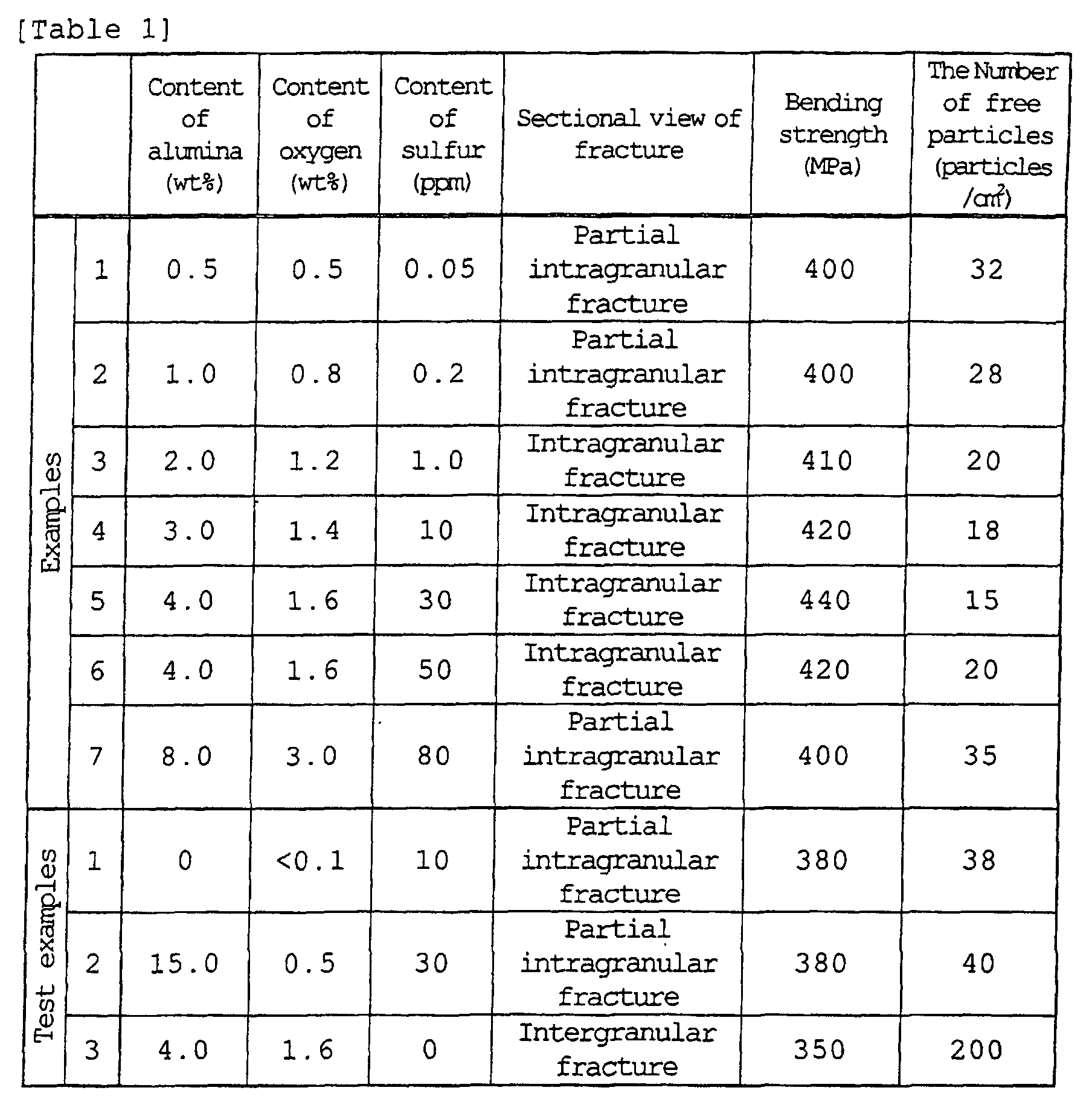
As is obvious from Table 1, when the content of sulfur
was too small, it was difficult to adjust the sectional view
of fracture of the ceramic substrate to a state of intragranular
fracture. It is assumed that this phenomenon is caused because
the effect of binding the grains drops when the content of sulfur
is too small.
On the other hand, when the content of oxygen is too much,
it was also difficult to bring most portions of the sectional
view of fracture of the ceramic substrate to a state of
intragranular fracture.
The number of the free particles generated in examples
1 to 7 was 40/ cm2 or less.
A composition containing: 100 parts by weight of aluminum
nitride powder (the average particle diameter: 1.1 µm) ; 4 parts
by weight of yttria (the average particle diameter: 0.4 µm) ;
12 parts by weight of acrylic binder; and alcohol was prepared.
By spray drying the obtained composition, granular powder was
produced. A formed body was produced by using the granular powder.
The obtained formed body was subjected to the firing process
at 1800 °C and under a pressure of 20 MPa. Thereafter, a ceramic
heater was produced in a manner substantially similar to that
of example 8.
A ceramic heater was produced in a manner similar to that
of example 8 except that the firing temperature was 1650 °C.
A ceramic heater was produced in a manner similar to that
of example 8 except that the firing temperature was 1950 °C.
Thereafter, a ceramic substrate was produced and a
resistance heating element and the like were formed therein in
a manner similar to that of example 11, whereby a ceramic heater
was obtained.
A composition containing: 100 parts by weight of aluminum
nitride powder (the average particle diameter: 1.1 µm) ; 4 parts
by weight of yttria (the average particle diameter: 0.4 µm) ;
12 parts by weight of acrylic binder; and alcohol was prepared.
By spray drying the obtained composition, granular powder was
produced. A formed body was produced by using the granular powder.
The obtained formed body was subjected to the firing process
at 1950 °C and under a pressure of 20 MPa. Thereafter, a ceramic
heater was produced in a manner substantially similar to that
of example 8 (that is, the only difference between example 8
and comparative example 5 was the abovementioned conditions in
preparing the formed body and firing).
In comparative example 6, a ceramic heater was produced
in a manner similar to that of example 8 except that the firing
temperature was 1950 °C.
For each of the ceramic heaters produced by examples 8
to 12 and comparative examples 1 to 6, measurement of the number
of the free particles, measurement of the average grain diameter
of the ceramic grains constituting the ceramic substrate and
observation of the sectional view of fracture thereof were
carried out according to the methods described below.
The SEM photograghs taken in the abovementioned
measurement and observation are shown in Figs. 25 to 30. Fig.
25 is a SEM photograph which shows the result of example 8. Fig.
26 is a SEM photograph which shows the result of example 9. Fig.
27 is a SEM photograph which shows the result of comparative
example 1. Fig. 28 is a SEM photograph which shows the result
of example 12. Fig. 29 is a SEM photograph which shows the result
of comparative example 5. Fig. 30 is a SEM photograph which shows
the result of comparative example 6.
Fig. 31 is a graph which shows the relationship between
the firing temperature (the amount of the sintering aid) and
the grain diameter.
For each of the ceramic substrates constituting these
ceramic heaters, the heat conductivity, the thermal expansion
coefficient, the bending strength and the fracture toughness
value were measured by the methods described below.
The results are shown in Table 2.
For each of the ceramic heaters according to examples 8
to 11 and comparative examples 1 to 4, the number of the free
particles thereof was measured by a method including the steps
of: placing the ceramic substrate with the heating face thereof
facing below; setting a silicon wafer under the lower side of
the ceramic substrate surface; carrying out a vibration test
at 10 to 55 Herz according to JIS C 0040; thereafter arbitrarily
photographing 10 sites at the silicon wafer by an electron
microscope, with observation; counting the number of the
particles whose particle diameter was 3 µm or more; dividing
the number of the free particles by the area of the photographed
field, thereby obtaining the number of the free particles per
the unit area.
For each of the ceramic heaters according to example 12
and comparative examples 5 and 6, the number of the free particles
thereof was measured by a method including the steps of: putting
a silicon wafer on each ceramic heater; applying a load of 50
kgf/cm2 on the silicon wafer; arbitrarily photographing 10 sites
at the silicon wafer by an electron microscope, with observation;
counting the number of the free particles whose particle diameter
was 2 µm or more; dividing the number of the free particles by
the area of the photographed field, thereby obtaining the number
of the free particles per the unit area.
The results thereof are shown in Table 2.
For each of the ceramic heaters according to the examples
and the comparative examples, the sectional view of fracture
thereof was observed with an electron microscope at a
magnification of 5000 times and the diameter of twenty,
arbitrarily chosen ceramic grains was each measured. The measured
diameter values were averaged.
For each of the ceramic heaters according to the examples
and the comparative examples, the sectional view of fracture
thereof was observed with an electron microscope at a
magnification of 8000 times and the state of the sectional view
of fracture, that is, whether the sectional view of fracture
exhibited the state of intragranular fracture or not, was
observed.
Thermal constant measuring device according to the Rigaku laser
flush method
LF/TCM-FA8510B
LF/TCM-FA8510B
| Temperature | Room temperature |
| Atmosphere | vacuum |
The temperature detection during the measurement of
specific heat was carried out by using a thermocouple attached
to the back surface of the sample with silver paste (a platinel).
The measurement of specific heat at the room temperature
was carried out in a state in which a light-receiving plate (glassy
carbon) was further attached to the upper surface of the sample
through silicon grease. The specific heat (Cp) of each sample
was obtained according to the calculation formula described
below.
Cp = {ΔO ΔT - CpG.C · W - CpS.G · WS.G } 1W
In the abovementioned calculation formula (1), ΔO
represents the input energy, ΔT represents the saturation value
of the temperature increase of the sample, CpG.C. represents the
specific heat of the glassy carbon, WG.C. represents the weight
of the glassy carbon, CpS.G. represents the specific heat of the
silicon grease, WS.G. represents the weight of the silicon grease,
W represents the weight of the sample.
For each of the ceramic substrates according to examples
8 to 12 and comparative examples 1 to 6, the strength thereof
was measured in a manner similar to that employed for the ceramic
heaters according to examples 1 to 7 and comparative examples
1 to 3. However, the present measurement was carried out in the
air at 25 °C.
The fracture toughness value was obtained by using a
Vickers hardness measuring device ("MVK-D" type manufactured
by Akashi Seisakusho Co.) , by pressing the indentator into the
surface of the sample, measuring the length of the generated
crack and performing the calculation according to the calculation
formula (3) described below.
Fracture toughness value
= 0.026 × E1/2 × 0.5 × P1/2 × a × C-3/2
where E represents the Young's modulus (3.18 × 10¹¹ Pa),
P represents the pressing load (98N) , "a" represents a half of
the average length of the indentation diagonal line (m), C
represents a half of the average length of cracks (m).

As is obvious from the results shown in Table 2, the average
grain diameter of the ceramic grains of each of the ceramic heaters
according to examples 8 to 11 was 3 µm or less and the sectional
view of fracture thereof exhibited the state of intragranular
fracture. When a silicon wafer was heated by using each of these
ceramic heaters, no free particles whose particle diameter was
3 µm or larger and only a very small amount of free particles
whose diameter was smaller than 3 µm were observed at the silicon
wafer, which allowed circuits and the like to be formed on the
silicon wafer in an excellent state. The bending strength of
these ceramic substrate was in a range of 471.6 to 550.5 MPa,
which was also excellent.
On the other hand, the average grain diameter of the ceramic
grains of each of the ceramic heaters according to comparative
examples 1 and 3 was 5.4 µm and 6.0 µm, respectively, both of
which exceeded 3 µm, and the sectional view of fracture thereof
exhibited the fracture at the grain boundary (intergranular
fracture). Further, when a silicon wafer was heated by using
each of these ceramic heaters, a number of free particles whose
particle diameter was 3 µm or larger was observed on the silicon
wafer, whereby failures such as short circuit occurred at the
circuit and the like formed on the silicon wafer, making some
samples unsuitable for actual use. In the ceramic heater
according to comparative example 4, the average grain diameter
thereof was 5.0 µm. In comparative example 2, the average grain
diameter was 0.6 µm but the sectional view of fracture thereof
exhibited interguranular fracture.
Further, in example 12, the average grain diameter of the
ceramic grains of the ceramic heater thereof was 2 µm or less
and the sectional view of fracture exhibited intragranular
fracture. When a silicon wafer was heated by using each of these
ceramic heaters, no free particles whose particle diameter was
2 µm or larger and only a very small amount of free particles
whose diameter was smaller than 2 µm were observed at the silicon
wafer, which allowed circuits and the like to be formed on the
silicon wafer in an excellent state.
On the other hand, the average grain diameter of the ceramic
grains of the ceramic heater according to comparative example
5 was 5.4 µm, which exceeded 2 µm, and the sectional view of
fracture thereof exhibited the intergranular fracture. When a
silicon wafer was heated by using this ceramic heater, a number
of free particles whose particle diameter was 2 µm or larger
were observed on the silicon wafer, whereby failures such as
short circuit occurred at the circuit and the like formed on
the silicon wafer, making some samples unsuitable for actual
use. Further, in comparative example 6, the average grain
diameter thereof was 2.5 µm, which was large.
Further, the bending strength of the ceramic substrate
according to examples 8 to 11 was in a range of 471.6 to 550.5
MPa, which was higher than the bending strength of the ceramic
substrate of the ceramic heaters according to comparative
examples 1 to 4.
Further, as shown in Fig. 31, as the firing temperature
increases and as the amount of the sintering aid is increased,
the average grain diameter becomes larger.
The content of oxygen of the ceramic substrate constituting
the electrostatic chuck having a resistance heating element
produced in such a manner was 1.6 weight %, and the content of
sulfur thereof was 30 ppm.
Further, the resistance heating element of the ceramic
substrate is energized, such that the temperature of the ceramic
substrate rose up to 400 °C and the resistance heating element
was operated. No leak current was observed, the strength at such
a high temperature of 400 °C was 400 Mpa, which is significantly
high and the ceramic substrate exhibited partial intragranular
fracture.
A paste was produced by mixing: 1000 parts by weight of
aluminum nitride powder (manufactured by Tokuyama Co., the
average particle diameter: 1.1 µm) which had been fired in the
air at 500 °C for 1 hour; 20 parts by weight of alumina (the
average particle diameter: 0.4µm) ; 115 parts by weight of acrylic
binder; 0.07 parts by weight of CaS; 0.03 parts by weight of
silica; 5 parts by weight of a dispersant; and 530 parts by weight
of alcohol comprising 1-butanol and ethanol. By using the
obtained paste and performing the forming process according to
the doctor blade method, a green sheet having a thickness of
0.47 mm was obtained. Thereafter, an electrostatic chuck was
produced in a manner similar to that of example 13.
A paste was produced by mixing: 1000 parts by weight of
aluminum nitride powder (manufactured by Tokuyama Co., the
average particle diameter: 1.1 µm) which had been fired in the
air at 500 °C for 1 hour; 20 parts by weight of alumina (the
average particle diameter: 0.4 µm) ; 115 parts by weight of acrylic
binder; 0.03 parts by weight of silica; 5 parts by weight of
a dispersant; and 530 parts by weight of alcohol comprising
1-butanol and ethanol. By using the obtained paste and performing
the forming process according to the doctor blade method, a green
sheet having a thickness of 0.47 mm was obtained.
The resistance heating element 25 of the electrostatic
chuck 201 fitted in this supporting case 41 is energized in order
to raise the temperature thereof and, at the same time , the coolant
was flowed through the supporting case, so that the temperature
of the electrostatic chuck 201 was controlled. The temperature
control was very excellently performed.
After implementing the processing steps of the
abovementioned (1) to (5) of example 15, nickel was flame sprayed
to the bottom face of the electrostatic chuck and then a
lead-tellurium based Peltier device was joined thereto, whereby
the electrostatic chuck 401 was obtained.
The electrostatic chuck 401 produced in such a manner had
excellent temperature-dropping property. When cooling was
performed by the Peltier device, the temperature dropped from
450 °C to 100 °C in three minutes.
A ceramic heater was produced in a manner similar to that
of example 1, except that the time duration of the hot-pressing
of aluminum nitride in the step (3) was changed to 10 hours.
(1) A paste was produced by mixing: 100 parts by weight of aluminum
nitride powder (manufactured by Tokuyama Co., the average
particle diameter: 1.1 µm) ; 4 parts by weight of yttria (the
average particle diameter: 0.4 µm) ; 11.5 parts by weight of
acrylic binder; 0.5 parts by weight of a dispersant; and 53 parts
by weight of alcohol comprising 1-butanol and ethanol. By using
the obtained paste and performing the forming process according
to the doctor blade method, a green sheet 50 having a thickness
of 0.47 mm was obtained. Thereafter, an electrostatic chuck was
produced in a manner similar to that of example 14.
An electrostatic chuck was produced in a manner similar
to that of example 15, except that the aluminum nitride powder
was not fired in the air and silica and the like was not added.
The content of oxygen in the aluminum nitride powder was
presumably 0.01 weight %.
An electrostatic chuck was produced in a manner similar
to that of example 15, except that 4 parts by weight of yttria
was added.
An electrostatic chuck was produced in a manner similar
to that of example 14, except that the electrostatic chuck had
a diameter of 330 mm and a thickness of 3 mm.
An electrostatic chuck was produced in a manner similar
to that of comparative example 7, except that the electrostatic
chuck had a diameter of 330 mm and a thickness of 3 mm.
An electrostatic chuck was produced in a manner similar
to that of comparative example 8, except that the electrostatic
chuck had a diameter of 330 mm and a thickness of 3 mm.
For each of the electrostatic chucks obtained by examples
14 to 17 and comparative examples 7 to 9 and the ceramic heater
obtained by test example 4, measurement of the number of free
particles and the bending strength, observation of the sectional
view of fracture and measurement of degree of warp and the oxygen
content were carried out by the methods similar to those employed
in examples 1 to 7. The results thereof are shown in Table 3.
Moreover, the degree of warp was measured by the method described
below only for the electrostatic chucks of example 14-1,
comparative examples 7-1 and 8-1.
Specifically, after raising the temperature of the ceramic
substrate to 600 °C in vacuum, the degree of warp of the ceramic
substrate was measured by using a laser displacement measuring
device. Moreover, the measurement was carried out in a range
of (diameter - 10 mm).

As is obvious from the SEM photograghs shown in Fig. 22
and Fig. 24, the ceramic substrate constituting the electrostatic
chuck according to example 14 exhibits a sectional view of
intragranular fracture, and the ceramic substrate constituting
the electrostatic chuck of comparative example 7 exhibits a
sectional view of intergranular fracture. Further, it is obvious
from Table 3 that the electrostatic chuck with a hot plate
according to examples 14 to 17 has excellent bending strength
at a high temperature and the number of free particles found
on the silicon wafer put on the electrostatic chuck is small.
The reason for the abovementioned high bending strength
at a high temperature is not clearly known. It is assumed that
the electrostatic chuck has excellent bending strength at a high
temperature because relatively few impurities such as oxygen
are present at the grain boundary and thus relatively few apparent
voids are found therein. In evaluation, the state of
"intragranular fracture" does not necessarily mean that all the
portions of the sectional view of fracture must show
intragranular fracture. As shown in an electron microscope (Fig.
22), when most portions of the sectional view of fracture exhibit
intragranular fracture, the state can be called "intragranular
fracture" if the sectional view includes some intergranular
fracture.
The content of oxygen of the ceramic substrate of the wafer
prober produced in such a manner as described above was 1.6 weight %
and the content of oxygen ion thereof was 30 ppm.
When the temperature of the ceramic substrate was raised
to 200 °C, no problems such as short circuit was observed. Further,
the bending strength of the ceramic substrate at 400 °C was 400
MPa, which was excellently high. Further, the sectional view
of fracture of the ceramic substrate exhibited partial
intragranular fracture.
When the obtained wafer prober having a heater was heated,
the temperature of the wafer prober reached 200 °C in about 20
seconds. The bending strength thereof at 400 °C was 400 MPa,
which was excellently high. Further, the sectional view of
fracture of the ceramic substrate exhibited intragranular
fracture.
An electrostatic chuck was produced in a manner similar
to that of example 20, except that the green sheet for the upper
layer was produced as follows. First, a paste was produced by
mixing: 100 parts by weight of aluminum nitride powder
(manufactured by Tokuyama Co., the average particle diameter:
0.6 µm) ; 0.2 parts by weight of yttria (the average particle
diameter: 0.4 µm) ; 11.5 parts by weight of acrylic binder; 0.5
parts by weight of a dispersant; and 53 parts by weight of alcohol
comprising 1-butanol and ethanol. By using the obtained paste
and performing the forming process according to the doctor blade
method, a green sheet for the upper layer having a thickness
of 0.47 mm was obtained.
An electrostatic chuck was produced in a manner similar
to that of example 20, except that the green sheet for the lower
layer was produced as follows. First, a paste was produced by
mixing: 1000 parts by weight of aluminum nitride powder
(manufactured by Tokuyama Co., the average particle diameter:
0.6 µm); 40 parts by weight of yttria (the average particle
diameter:0.4 µm) ; 115 parts by weight of acrylic binder; 0.002
parts by weight of boron nitride; 0.05 parts by weight of silica;
0.001 parts by weight of Na2O; 5 parts by weight of a dispersant;
and 530 parts by weight of alcohol comprising 1-butanol and
ethanol. By using the obtained paste and performing the forming
process according to the doctor blade method, a green sheet for
the lower layer having a thickness of 0.47 mm was obtained.
An electrostatic chuck was produced in a manner similar
to that of example 22, except that the green sheet for the upper
layer was produced as follows. First, a paste was prepared by
mixing: 100 parts by weight of aluminum nitride powder
(manufactured by Tokuyama Co., the average particle diameter:
0.6 µm); 0.2 parts by weight of yttria (the average particle
diameter: 0.4 µm) ; 11.5 parts by weight of acrylic binder; 0.5
parts by weight of a dispersant; and 53 parts by weight of alcohol
comprising 1-butanol and ethanol. By using the obtained paste
and performing the forming process according to the doctor blade
method, a green sheet for the upper layer having a thickness
of 0.47 mm was obtained.
First, a paste was prepared mixing: 100 parts by weight
of aluminum nitride powder (the average particle diameter: 0.6
µm) ; 0.3 parts by weight of yttria (the average particle diameter:
0.4 µm) ; 12 parts by weight of an acrylic binder; and alcohol.
By using the obtained paste and performing the forming process
according to the doctor blade method, a green sheet having a
thickness of 0.47 mm was obtained. Then, an electrostatic chuck
was produced in a manner similar to that of comparative example
10, except that the green sheet was hot-pressed for 3 hours at
1700 °C and at a pressure of 20 MPa (200 kgf/cm2).
For each of electrostatic chucks produced in examples 20
to 23 and comparative examples 10 and 11, counting of the number
of free particles, observation of the sectional view of fracture,
measurement of the porosity, measurement of temperature
distribution after the temperature of the ceramic substrate
reached 400 °C, and an insulation test of the conductor circuit
in the ceramic substrate, were carried out. In addition,
presence/absence of occurrence of short circuit between the
conductor circuits was checked.
The results thereof are shown in Table 4 below.
The number of the free particles was measured by a method
including the steps of: setting a silicon wafer on each
electrostatic chuck; applying a load of 50 kgf/cm2 thereon;
arbitrarily photographing 10 sites at the silicon wafer by an
electron microscope, with observation; counting the number of
the free particles whose particle diameter was 2 µm or more;
dividing the number of the particles by the area of the
photographed field, thereby obtaining the number of the particles
per the unit area.
For each of the electrostatic chucks, the sectional view
of fracture thereof was observed with an electron microscope
at a magnification of 5000 times and the state of the sectional
view of fracture, that is, whether the sectional view of fracture
exhibited the state of intragranular fracture or not, was
observed. Fig. 32 is a photograph taken by a scanning electron
microscope (SEM) which shows a sectional view of fracture in
the vicinity of the upper surface (the upper layer) of an
electrostatic chuck according to example 20. Fig. 33 is a
photograph taken by a scanning electron microscope (SEM) which
shows a sectional view of fracture at the lower surface of the
electrostatic chuck according to example 20.
Each of the electrostatic chucks according to examples
20 to 23 and comparative examples 10 to 11 was energized and
the temperature thereof was raised to 400 °C. Thereafter, the
difference in temperature at the heating face was measured by
a thermoviewer ("IR162012-0012" manufactured by Nihon Datum
Co. ) .
The state of insulation between the conductor circuits
provided in the ceramic substrate (that is, whether insulation
is being maintained therebetween or not) was checked by using
a tester, whereby presence/absence of occurrence of short circuit
was checked.
Measurement of the porosity was performed according to
the Archimedes' method. Moreover, the measurement of the pore
diameter at the upper layer portion of the electrostatic chuck
was carried out in a method in which the upper layer portion
thereof was thinly peeled or separated.

As is obvious from the results shown in Table 4, the
sectional view of fracture in the vicinity of the upper portion
surface (the upper layer) of the electrostatic chuck according
to examples 20 to 23 exhibited the state of intragranular fracture.
Accordingly, the number of free particles observed in the
vicinity of the surface of the silicon wafer and the like which
had been treated was relatively small.
On the other hand, the sectional view of fracture of the
lower portion (the lower layer) exhibited the state of
intergranular fracture. Further, the porosity of the lower layer
was lower than that of the upper layer. Accordingly, the results
of the insulation test of the conductor circuit in the ceramic
substrates were unanimously excellent and no short circuit was
observed therein.
In comparative example 10, the sectional view of fracture
exhibited the state of intergranular fracture at both the upper
and lower layers. In this comparative example, the porosity of
the ceramic substrate as a whole was relatively low and the result
of the insulation test of the conductor circuit in the ceramic
substrate was generally good, thereby avoiding occurrence of
short circuit between the conductor circuits. However, in this
case, the number of free particles observed on the surface of
the silicon wafer and the like which had been treated was
relatively large, whereby short circuits, disconnection and the
like occurred in the conductor circuit of the silicon wafer.
Further, the sectional view of fracture of the
electrostatic chuck according to comparative example 11
exhibited the state of intragranular fracture at both the upper
and lower layers. Therefore, the number of free particles
observed on the surface of the silicon wafer and the like which
had been treated was relatively small and occurrence of short
circuit, disconnection and the like was not observed in the
conductor circuits of the silicon wafer. However, in this case,
the porosity of the electrostatic chuck was high as a whole and
the insulation between the conductor circuits in the ceramic
substrate was not reliably maintained, whereby occurrence of
short circuit was observed.
As described above, the aluminum nitride sintered body
of the first aspect of the present invention contains sulfur.
As a result, the binding force between the ceramic grains is
strong and the aluminum nitride sintered body has excellent
mechanical strength, whereby coming-off of the ceramic particles
from the surface and/or the side face of the aluminum nitride
sintered body is suppressed and generation of free particles
can be significantly prevented.
The aluminum nitride sintered body of the second aspect
of the present invention exhibits intragranular fracture at the
sectional view of fracture thereof. In addition, the average
grain diameter of the aluminum nitride sintered body is adjusted
so as to be 3 µm or less. Accordingly, coming-off of particles
is hardly observed. Further, as there exist hardly any barriers
between the grains of the aluminum nitride sintered body, the
strength thereof at a high temperature is significantly enhanced.
The ceramic substrate of the third aspect of the present
invention is sintered such that the sectional view of fracture
thereof exhibits intragranular fracture. As a result, the ceramic
substrate is excellent in the properties at a high temperature,
generates a relatively small number of free particles which
attach to the silicon wafer and the like and thus can be most
suitably used as a ceramic substrate for a semiconductor
producing/examining device.
In the ceramic substrate of the fourth aspect of the present
invention, the average grain diameter of the ceramic grain of
the ceramic substrate is adjusted so as to be 2 µm or less.
Accordingly, the sectional view of fracture thereof is likely
to exhibit intragranular fracture and coming-off of particles
is not likely to happen. Further, as the diameter of the free
particles which come off is small (2 µm or less) , the silicon
wafer and the like is prevented from being contaminated.
Therefore, the ceramic substrate of the present invention can
be most preferably used as a ceramic substrate for a semiconductor
producing/examining device.
The ceramic substrate for a semiconductor
producing/examining device of the fifth aspect of the present
invention is a ceramic substrate including a conductor formed
inside thereof. The ceramic layer which includes the conductor
and the layers located lower than the conductor (that is, the
lower layer) exhibits the state of intergranular fracture at
the time of fracture. Another ceramic layer (the upper layer)
exhibits the state of intragranular fracture at the time of
fracture. Accordingly, generation of free particles as a result
of coming-off of the ceramic particles is not likely to occur
at the substrate surface on which the material to be treated
is loaded, whereby short circuit, disconnection and the like
are not likely to happen between the conductor circuits formed
on the object to be treated (for instance, a silicon wafer).
Further, as the porosity is relatively small between the
conductor circuits of the ceramic substrate, short circuits are
not likely to occur between the conductor circuits and thus the
substrate reliably function in an excellent manner.
The electrostatic chuck of the sixth aspect of the present
invention is the electrostatic chuck comprising the
electrostatic electrode and the resistance heating element
formed inside the ceramic substrate. The ceramic layer which
includes the electrostatic electrode and the layers located lower
than the electrostatic electrode (that is, the lower layer)
exhibits the state of intergranular fracture at the time of
fracture. Another ceramic layer (the upper layer) exhibits the
state of intragranular fracture at the time of fracture.
Accordingly, grains constituting the upper layer are firmly bound
to each other and the ceramic particles are not likely to come
off from the surface of the upper layer, whereby coming-off of
particles from the dielectric film surface and attachment of
the generated free particles to the object to be treated (such
as a silicon wafer) can be prevented and thus occurrence of
adhesion failure between the object to be treated and the
electrostatic chuck can be prevented. Further, the lower ceramic
layer exhibits the state of intergranular fracture at the time
of fracture and has a relatively low porosity, whereby occurrence
of short circuit: between the electrostatic electrodes; between
the resistance heating elements; or between the electrostatic
electrode and the resistance heating element of the lower layer
can be prevented. In case that a RF electrode is present in the
electrostatic chuck, occurrence of short circuit between the
electrostatic electrode and the RF electrode and between the
RF electrode and the resistance heating element can also be
prevented, whereby the electrostatic chuck can function in an
excellent manner.
Claims (16)
- An aluminum nitride sintered body containing sulfur.
- The aluminum nitride sintered body according to claim 1,
wherein the content of said sulfur is in a range of 0.05 to 200 ppm. - The aluminum nitride sintered body according to claim 1 or 2,
wherein said aluminum nitride sintered body contains oxygen. - An aluminum nitride sintered body,
wherein said aluminum nitride sintered body exhibits a state of intragranular fracture at the time of fracture and the average grain diameter of a ceramic grain thereof is 3 µm or less. - A ceramic substrate having a conductor inside thereof or on the surface thereof,
wherein said ceramic substrate has been sintered such that a sectional view of fracture thereof exhibits intragranular fracture. - The ceramic substrate according to claim 5,
wherein the average grain diameter of a ceramic grain thereof is 3 µm or less. - The ceramic substrate according to claim 5 or 6,
wherein said ceramic substrate comprises nitride ceramic and said nitride ceramic contains sulfur therein. - The ceramic substrate according to any of claims 5 to 7,
wherein the content of said sulfur is in a range of 0.05 to 200 ppm. - The ceramic substrate according to any of claims 5 to 8,
wherein said ceramic substrate contains oxygen. - A ceramic heater,
wherein the ceramic substrate according to any of claims 5 to 9 is used. - An electrostatic chuck,
wherein the ceramic substrate according to any of claims 5 to 9 is used. - A ceramic substrate having a conductor inside thereof or on the surface thereof,
wherein the average grain diameter of the ceramic grain of said ceramic substrate is 2 µm or less. - A ceramic heater,
wherein the ceramic substrate according to claim 12 is used. - An electrostatic chuck,
wherein the ceramic substrate according to claim 12 is used. - A ceramic substrate having a conductor formed inside thereof for a semiconductor producing/examining device,
wherein:a ceramic layer including said conductor and the vicinity thereof and a ceramic layer located lower than said conductor exhibit a state of intergranular fracture at the time of fracture; anda ceramic layer other than said ceramic layers exhibits a state of intragranular fracture at the time of fracture. - An electrostatic chuck having an electrostatic electrode and a resistance heating element formed inside a ceramic substrate thereof,
wherein:a ceramic layer including said conductor and the vicinity thereof and a ceramic layer located lower than said conductor exhibit a state of intergranular fracture at the time of fracture; anda ceramic layer other than said ceramic layers exhibits a state of intragranular fracture at the time of fracture.
Applications Claiming Priority (11)
| Application Number | Priority Date | Filing Date | Title |
|---|---|---|---|
| JP2000048262 | 2000-02-24 | ||
| JP2000048338 | 2000-02-24 | ||
| JP2000048338 | 2000-02-24 | ||
| JP2000048262A JP2001233675A (en) | 2000-02-24 | 2000-02-24 | Aluminum nitride sintered body and ceramic substrate |
| JP2000202826A JP2002025749A (en) | 2000-07-04 | 2000-07-04 | Ceramic heater |
| JP2000020226 | 2000-07-04 | ||
| JP2000036168 | 2000-11-28 | ||
| JP2000361768A JP2002164422A (en) | 2000-11-28 | 2000-11-28 | Aluminum nitride sintered body and ceramic substrate |
| JP2000036741 | 2000-12-01 | ||
| JP2000367541A JP2002170870A (en) | 2000-12-01 | 2000-12-01 | Ceramic substrate and electrostatic chuck for semiconductor fabrication/inspection equipment |
| PCT/JP2001/001406 WO2001062686A1 (en) | 2000-02-24 | 2001-02-26 | Aluminum nitride sintered compact, ceramic substrate, ceramic heater and electrostatic chuck |
Publications (2)
| Publication Number | Publication Date |
|---|---|
| EP1191002A1 true EP1191002A1 (en) | 2002-03-27 |
| EP1191002A4 EP1191002A4 (en) | 2005-01-26 |
Family
ID=27531425
Family Applications (1)
| Application Number | Title | Priority Date | Filing Date |
|---|---|---|---|
| EP01906299A Withdrawn EP1191002A4 (en) | 2000-02-24 | 2001-02-26 | SINTERED ALUMINUM NITRIDE PIECE, CERAMIC SUBSTRATE, CERAMIC HEATING BODY, AND ELECTROSTATIC CHUCK |
Country Status (3)
| Country | Link |
|---|---|
| US (3) | US6861165B2 (en) |
| EP (1) | EP1191002A4 (en) |
| WO (1) | WO2001062686A1 (en) |
Cited By (2)
| Publication number | Priority date | Publication date | Assignee | Title |
|---|---|---|---|---|
| DE10312626B4 (en) * | 2003-03-21 | 2014-12-24 | Infineon Technologies Ag | Electrostatic carrier |
| EP3873173A1 (en) | 2020-02-26 | 2021-09-01 | SunFire GmbH | Gas heater heating element manufacturing method and gas heater heating element |
Families Citing this family (70)
| Publication number | Priority date | Publication date | Assignee | Title |
|---|---|---|---|---|
| US6900149B1 (en) * | 1999-09-06 | 2005-05-31 | Ibiden Co., Ltd. | Carbon-containing aluminum nitride sintered compact and ceramic substrate for use in equipment for manufacturing or inspecting semiconductor |
| WO2001062686A1 (en) * | 2000-02-24 | 2001-08-30 | Ibiden Co., Ltd. | Aluminum nitride sintered compact, ceramic substrate, ceramic heater and electrostatic chuck |
| JP2001247382A (en) * | 2000-03-06 | 2001-09-11 | Ibiden Co Ltd | Ceramic substrate |
| EP1233651A1 (en) * | 2000-04-07 | 2002-08-21 | Ibiden Co., Ltd. | Ceramic heater |
| JP3565496B2 (en) * | 2000-04-13 | 2004-09-15 | イビデン株式会社 | Ceramic heater, electrostatic chuck and wafer prober |
| US7071551B2 (en) * | 2000-05-26 | 2006-07-04 | Ibiden Co., Ltd. | Device used to produce or examine semiconductors |
| JP3516392B2 (en) * | 2000-06-16 | 2004-04-05 | イビデン株式会社 | Hot plate for semiconductor manufacturing and inspection equipment |
| WO2002003435A1 (en) * | 2000-07-04 | 2002-01-10 | Ibiden Co., Ltd. | Hot plate for semiconductor manufacture and testing |
| WO2002009171A1 (en) * | 2000-07-25 | 2002-01-31 | Ibiden Co., Ltd. | Ceramic substrate for semiconductor manufacture/inspection apparatus, ceramic heater, electrostatic clampless holder, and substrate for wafer prober |
| WO2002047129A1 (en) | 2000-12-05 | 2002-06-13 | Ibiden Co., Ltd. | Ceramic substrate for semiconductor manufacturing and inspecting devices, and method of manufacturing the ceramic substrate |
| US20040206747A1 (en) * | 2001-04-11 | 2004-10-21 | Yasutaka Ito | Ceramic heater for semiconductor manufacturing/inspecting apparatus |
| US20040239717A1 (en) * | 2003-02-26 | 2004-12-02 | Kyocera Corporation | Alumina sintered body and ink-jet recording head structure |
| DE10320384B3 (en) * | 2003-05-06 | 2005-02-10 | Leybold Optics Gmbh | Heating unit, for vacuum deposition assembly, has electrical heating wire embedded in non-conductive ceramic material with electrical contact through contact pins with shrouding for connection to a high tension supply |
| KR100832684B1 (en) * | 2003-07-08 | 2008-05-27 | 가부시끼가이샤 퓨처 비전 | Substrate stage, electrode used for the substrate stage, and treating apparatus having the substrate stage and the electrode |
| KR100756776B1 (en) * | 2003-10-31 | 2007-09-07 | 가부시끼가이샤 도꾸야마 | Aluminum nitride joined article and method for manufacture thereof |
| KR100555222B1 (en) * | 2003-11-18 | 2006-03-03 | 한국표준과학연구원 | Surface modification method of oxide ceramics using glass and surface modified oxide ceramics |
| JP4321855B2 (en) * | 2003-12-11 | 2009-08-26 | 日本碍子株式会社 | Ceramic chuck |
| US7220497B2 (en) * | 2003-12-18 | 2007-05-22 | Lam Research Corporation | Yttria-coated ceramic components of semiconductor material processing apparatuses and methods of manufacturing the components |
| JP4266886B2 (en) * | 2004-06-21 | 2009-05-20 | 株式会社ソディック | Ceramic element and manufacturing method thereof |
| KR100550019B1 (en) * | 2004-07-21 | 2006-02-08 | 주식회사 코미코 | Ceramic electrostatic chuck device having arc preventing edge protrusion and manufacturing method thereof |
| US20060088692A1 (en) * | 2004-10-22 | 2006-04-27 | Ibiden Co., Ltd. | Ceramic plate for a semiconductor producing/examining device |
| US7300707B2 (en) * | 2004-10-25 | 2007-11-27 | Creative Technology Corporation | Aluminium composite structure having a channel therein and method of manufacturing the same |
| JP2007042910A (en) * | 2005-08-04 | 2007-02-15 | Sumitomo Electric Ind Ltd | Wafer prober chuck top and wafer prober mounted therewith |
| JP5161450B2 (en) * | 2005-09-30 | 2013-03-13 | 財団法人高知県産業振興センター | Plasma CVD apparatus and plasma surface treatment method |
| KR101329630B1 (en) * | 2006-04-13 | 2013-11-14 | 신에쓰 가가꾸 고교 가부시끼가이샤 | Heating element |
| US8226769B2 (en) * | 2006-04-27 | 2012-07-24 | Applied Materials, Inc. | Substrate support with electrostatic chuck having dual temperature zones |
| US20070251456A1 (en) * | 2006-04-27 | 2007-11-01 | Applied Materials, Inc., A Delaware Corporation | Composite heater and chill plate |
| US7696455B2 (en) * | 2006-05-03 | 2010-04-13 | Watlow Electric Manufacturing Company | Power terminals for ceramic heater and method of making the same |
| US20070284356A1 (en) * | 2006-06-09 | 2007-12-13 | Carol Findlay | Warming blanket with independent energy source |
| JP5137362B2 (en) * | 2006-09-12 | 2013-02-06 | イビデン株式会社 | Structure comprising a metal substrate and an inorganic material surface layer |
| JP2008108703A (en) * | 2006-09-28 | 2008-05-08 | Covalent Materials Corp | Planar heater and semiconductor heat treatment apparatus provided with the heater |
| US8573836B2 (en) * | 2006-10-26 | 2013-11-05 | Tokyo Electron Limited | Apparatus and method for evaluating a substrate mounting device |
| US7928029B2 (en) * | 2007-02-20 | 2011-04-19 | Corning Incorporated | Refractory ceramic composite and method of making |
| US20080226838A1 (en) * | 2007-03-12 | 2008-09-18 | Kochi Industrial Promotion Center | Plasma CVD apparatus and film deposition method |
| CN101409961B (en) * | 2007-10-10 | 2010-06-16 | 清华大学 | Surface heat light source, its preparation method and its application method for heating objects |
| CN101400198B (en) * | 2007-09-28 | 2010-09-29 | 北京富纳特创新科技有限公司 | Surface heat light source, its preparation method and its application method for heating objects |
| CN101409962B (en) * | 2007-10-10 | 2010-11-10 | 清华大学 | Surface heat light source and preparation method thereof |
| JP4533926B2 (en) * | 2007-12-26 | 2010-09-01 | 財団法人高知県産業振興センター | Film forming apparatus and film forming method |
| US8993939B2 (en) * | 2008-01-18 | 2015-03-31 | Momentive Performance Materials Inc. | Resistance heater |
| US20100122980A1 (en) * | 2008-06-13 | 2010-05-20 | Tsinghua University | Carbon nanotube heater |
| US20100000669A1 (en) * | 2008-06-13 | 2010-01-07 | Tsinghua University | Carbon nanotube heater |
| US20100126985A1 (en) * | 2008-06-13 | 2010-05-27 | Tsinghua University | Carbon nanotube heater |
| WO2010090948A1 (en) * | 2009-02-04 | 2010-08-12 | Mattson Technology, Inc. | Electrostatic chuck system and process for radially tuning the temperature profile across the surface of a substrate |
| US8580593B2 (en) * | 2009-09-10 | 2013-11-12 | Micron Technology, Inc. | Epitaxial formation structures and associated methods of manufacturing solid state lighting devices |
| JP5412270B2 (en) * | 2009-12-28 | 2014-02-12 | 株式会社日立ハイテクノロジーズ | Scanning electron microscope |
| US8547005B1 (en) | 2010-05-18 | 2013-10-01 | Superior Technical Ceramics, Inc. | Multi-layer heater for an electron gun |
| US20140251214A1 (en) * | 2013-03-06 | 2014-09-11 | Applied Materials, Inc. | Heated substrate support with flatness control |
| EP3041039B1 (en) * | 2013-08-26 | 2022-01-05 | KYOCERA Corporation | Sample-retainer |
| CN107207367A (en) | 2014-05-07 | 2017-09-26 | 摩根先进陶瓷公司 | For manufacturing the large-scale improved method for burning object altogether |
| JP6219229B2 (en) * | 2014-05-19 | 2017-10-25 | 東京エレクトロン株式会社 | Heater feeding mechanism |
| EP3252810B1 (en) * | 2015-01-29 | 2020-01-08 | Kyocera Corporation | Circuit board and electronic device |
| JP6690918B2 (en) * | 2015-10-16 | 2020-04-28 | 日本特殊陶業株式会社 | Heating member, electrostatic chuck, and ceramic heater |
| JP6673466B2 (en) * | 2016-03-22 | 2020-03-25 | 株式会社村田製作所 | Ceramic electronic component and method of manufacturing ceramic electronic component |
| KR102377658B1 (en) * | 2016-03-23 | 2022-03-24 | 엔지케이 인슐레이터 엘티디 | Cordierite sintered body and production thereof and composite substrate |
| CN109156050A (en) * | 2016-04-07 | 2019-01-04 | 美题隆公司 | Beryllium oxide integral resistance heater |
| US10636690B2 (en) * | 2016-07-20 | 2020-04-28 | Applied Materials, Inc. | Laminated top plate of a workpiece carrier in micromechanical and semiconductor processing |
| JP6758143B2 (en) * | 2016-09-29 | 2020-09-23 | 日本特殊陶業株式会社 | Heating device |
| US10679873B2 (en) * | 2016-09-30 | 2020-06-09 | Ngk Spark Plug Co., Ltd. | Ceramic heater |
| JP6927851B2 (en) | 2017-10-30 | 2021-09-01 | モメンティブ・クオーツ・ジャパン合同会社 | Heater and its manufacturing method |
| KR20200143691A (en) | 2018-03-27 | 2020-12-24 | 에스씨피 홀딩스 언 어숨드 비지니스 네임 오브 나이트라이드 이그나이터스 엘엘씨 | High temperature surface igniter for cooktop |
| US12020956B2 (en) | 2019-05-03 | 2024-06-25 | Therm-X Of California, Inc. | High temperature aluminum nitride heater pedestal with multi-zone capability |
| WO2021053724A1 (en) * | 2019-09-17 | 2021-03-25 | 株式会社Kokusai Electric | Substrate processing apparatus, susceptor cover, and method for manufacturing semiconductor apparatus |
| TW202518671A (en) | 2019-10-11 | 2025-05-01 | 美商應用材料股份有限公司 | Pedestal heater for spatial multi-wafer processing tool |
| JP7465771B2 (en) * | 2020-09-15 | 2024-04-11 | 日本碍子株式会社 | Compound sintered body, semiconductor manufacturing equipment member, and method for manufacturing compound sintered body |
| KR102843910B1 (en) * | 2021-05-04 | 2025-08-07 | 와틀로 일렉트릭 매뉴팩츄어링 컴파니 | Metal heater assembly with resistance heater installed |
| DE102021123004A1 (en) * | 2021-09-06 | 2023-03-09 | Specs Surface Nano Analysis Gmbh | Sample carrier and sample holder for holding a sample in an evacuated environment or a gas atmosphere |
| KR20230145459A (en) * | 2022-03-30 | 2023-10-17 | 엔지케이 인슐레이터 엘티디 | Materials for semiconductor manufacturing equipment |
| WO2025254805A1 (en) * | 2024-06-05 | 2025-12-11 | Heraeus Covantics North America Llc | Process for producing a sintered layered body by controlling the sulfur content of a powder employed |
| WO2025254804A1 (en) * | 2024-06-05 | 2025-12-11 | Heraeus Covantics North America Llc | Process for producing a sintered layered body by controlling the carbon content of a powder employed |
| CN119735442B (en) * | 2024-11-11 | 2025-12-05 | 山东大学 | An assembly method for low-loss sintering and purification of aluminum nitride raw materials |
Family Cites Families (81)
| Publication number | Priority date | Publication date | Assignee | Title |
|---|---|---|---|---|
| US256356A (en) * | 1882-04-11 | Cultivator-tooth | ||
| US256700A (en) * | 1882-04-18 | Melvin jincks | ||
| US257463A (en) * | 1882-05-09 | Half to hiram edgar ketohum | ||
| US6635853B2 (en) * | 1909-08-09 | 2003-10-21 | Ibiden Co., Ltd. | Hot plate unit |
| JPS6060983A (en) * | 1983-09-08 | 1985-04-08 | 株式会社デンソー | Ceramic heater and manufacture |
| JPH075371B2 (en) | 1984-12-17 | 1995-01-25 | ティーディーケイ株式会社 | Aluminum nitride sintered body and manufacturing method thereof |
| US5154863A (en) | 1985-10-31 | 1992-10-13 | Kyocera Corporation | Aluminum nitride-based sintered body and process for the production thereof |
| DE3608326A1 (en) * | 1986-03-13 | 1987-09-17 | Kempten Elektroschmelz Gmbh | PRACTICAL, PORE-FREE SHAPED BODIES MADE OF POLYCRISTALLINE ALUMINUM NITRIDE AND METHOD FOR THE PRODUCTION THEREOF WITHOUT THE USE OF SINTER AUXILIARIES |
| JPS6311575A (en) | 1986-07-01 | 1988-01-19 | 旭硝子株式会社 | Manufacture of aluminum nitride sintered body |
| EP0393524A3 (en) | 1989-04-17 | 1993-02-10 | Kawasaki Steel Corporation | Method of making a sintered body of aluminium nitride |
| JPH02275765A (en) | 1989-04-17 | 1990-11-09 | Kawasaki Steel Corp | Production of sintered aluminum nitride |
| JP2968539B2 (en) * | 1989-06-30 | 1999-10-25 | 株式会社東芝 | Method for manufacturing aluminum nitride structure |
| US5350720A (en) * | 1991-03-18 | 1994-09-27 | Shin-Etsu Chemical Co., Ltd. | Triple-layered ceramic heater |
| JPH04317402A (en) | 1991-04-16 | 1992-11-09 | Sumitomo Chem Co Ltd | Aluminum nitride power and its production |
| JPH0597523A (en) | 1991-10-03 | 1993-04-20 | Sumitomo Chem Co Ltd | Production of sintered aluminum nitride |
| JPH05117039A (en) | 1991-10-29 | 1993-05-14 | Sumitomo Chem Co Ltd | Aluminum nitride powder and method for producing the same |
| JPH05147910A (en) | 1991-11-25 | 1993-06-15 | Sumitomo Chem Co Ltd | Aluminum nitride powder and method for producing the same |
| JPH06206772A (en) | 1992-11-18 | 1994-07-26 | Toshiba Corp | Aluminum nitride sintered compact and ceramic circuit substrate |
| JPH06191955A (en) | 1992-12-22 | 1994-07-12 | Matsushita Electric Works Ltd | Production of aluminum mitride sintered compact |
| JP3152857B2 (en) | 1995-02-28 | 2001-04-03 | 京セラ株式会社 | Electrostatic chuck |
| JP3501317B2 (en) | 1995-07-21 | 2004-03-02 | 日産自動車株式会社 | High thermal conductivity silicon nitride sintered body and insulating substrate made of silicon nitride sintered body |
| JP3389384B2 (en) | 1995-10-31 | 2003-03-24 | 京セラ株式会社 | Aluminum nitride substrate |
| JP3693077B2 (en) | 1996-09-02 | 2005-09-07 | 信越化学工業株式会社 | Electrostatic chuck |
| JP3145664B2 (en) | 1997-08-29 | 2001-03-12 | 京セラ株式会社 | Wafer heating device |
| JPH11111431A (en) | 1997-09-29 | 1999-04-23 | Kyocera Corp | Ceramic heater and method of manufacturing the same |
| JPH11228234A (en) | 1998-02-17 | 1999-08-24 | Kobe Steel Ltd | Sintered product having excellent corrosion resistance and heat conductivity |
| JPH11236270A (en) | 1998-02-25 | 1999-08-31 | Kyocera Corp | Silicon nitride substrate and method of manufacturing the same |
| JP2000048262A (en) | 1998-07-30 | 2000-02-18 | Nippon Syst Akad:Kk | Goods storage management system for shop |
| WO2000069219A1 (en) * | 1999-05-07 | 2000-11-16 | Ibiden Co., Ltd. | Hot plate and method of producing the same |
| US6835916B2 (en) * | 1999-08-09 | 2004-12-28 | Ibiden, Co., Ltd | Ceramic heater |
| JP2001118664A (en) | 1999-08-09 | 2001-04-27 | Ibiden Co Ltd | Ceramic heater |
| JP3381909B2 (en) * | 1999-08-10 | 2003-03-04 | イビデン株式会社 | Ceramic heater for semiconductor manufacturing and inspection equipment |
| US6717116B1 (en) * | 1999-08-10 | 2004-04-06 | Ibiden Co., Ltd. | Semiconductor production device ceramic plate |
| US6900149B1 (en) * | 1999-09-06 | 2005-05-31 | Ibiden Co., Ltd. | Carbon-containing aluminum nitride sintered compact and ceramic substrate for use in equipment for manufacturing or inspecting semiconductor |
| EP1199908A4 (en) * | 1999-10-22 | 2003-01-22 | Ibiden Co Ltd | CERAMIC HEATING PLATE |
| US6632512B1 (en) * | 1999-11-10 | 2003-10-14 | Ibiden Co., Ltd. | Ceramic substrate |
| ATE301916T1 (en) | 1999-11-19 | 2005-08-15 | Ibiden Co Ltd | CERAMIC HEATER |
| WO2001041508A1 (en) | 1999-11-30 | 2001-06-07 | Ibiden Co., Ltd. | Ceramic heater |
| EP1383167A1 (en) * | 1999-12-09 | 2004-01-21 | Ibiden Co., Ltd. | Ceramic plate for semiconductor producing/inspecting apparatus |
| JP2001237053A (en) * | 1999-12-14 | 2001-08-31 | Ibiden Co Ltd | Ceramic heater and support pins for semiconductor manufacturing and inspection equipment |
| US20040016746A1 (en) * | 1999-12-29 | 2004-01-29 | Ibiden Co., Ltd. | Ceramic heater |
| JP3228923B2 (en) * | 2000-01-18 | 2001-11-12 | イビデン株式会社 | Ceramic heater for semiconductor manufacturing and inspection equipment |
| JP3228924B2 (en) * | 2000-01-21 | 2001-11-12 | イビデン株式会社 | Ceramic heater for semiconductor manufacturing and inspection equipment |
| EP1193233A1 (en) * | 2000-02-07 | 2002-04-03 | Ibiden Co., Ltd. | Ceramic substrate for semiconductor production/inspection device |
| US7011874B2 (en) * | 2000-02-08 | 2006-03-14 | Ibiden Co., Ltd. | Ceramic substrate for semiconductor production and inspection devices |
| US6686570B2 (en) * | 2000-02-10 | 2004-02-03 | Tokyo Electron Limited | Hot plate unit |
| WO2001062686A1 (en) * | 2000-02-24 | 2001-08-30 | Ibiden Co., Ltd. | Aluminum nitride sintered compact, ceramic substrate, ceramic heater and electrostatic chuck |
| JP2001244320A (en) | 2000-02-25 | 2001-09-07 | Ibiden Co Ltd | Ceramic substrate and method of manufacturing the same |
| US20030098299A1 (en) * | 2000-03-06 | 2003-05-29 | Ibiden Co., Ltd. | Ceramic heater |
| WO2001066488A1 (en) * | 2000-03-07 | 2001-09-13 | Ibiden Co., Ltd. | Ceramic substrate for manufacture/inspection of semiconductor |
| JP2001253777A (en) * | 2000-03-13 | 2001-09-18 | Ibiden Co Ltd | Ceramic substrate |
| US20040074586A1 (en) * | 2000-03-15 | 2004-04-22 | Yasuji Hiramatsu | Method of producing electrostatic chucks and method of producing ceramic heaters |
| EP1233651A1 (en) * | 2000-04-07 | 2002-08-21 | Ibiden Co., Ltd. | Ceramic heater |
| US20040149718A1 (en) * | 2000-04-07 | 2004-08-05 | Yasutaka Ito | Ceramic heater |
| US20030160042A1 (en) * | 2000-04-10 | 2003-08-28 | Yasuji Hiramatsu | Ceramic board |
| JP3565496B2 (en) * | 2000-04-13 | 2004-09-15 | イビデン株式会社 | Ceramic heater, electrostatic chuck and wafer prober |
| US6887316B2 (en) * | 2000-04-14 | 2005-05-03 | Ibiden Co., Ltd. | Ceramic heater |
| JP2001302330A (en) * | 2000-04-24 | 2001-10-31 | Ibiden Co Ltd | Ceramic substrate |
| WO2001084888A1 (en) * | 2000-04-29 | 2001-11-08 | Ibiden Co., Ltd. | Ceramic heater and method of controlling temperature of the ceramic heater |
| WO2001084885A1 (en) * | 2000-05-02 | 2001-11-08 | Ibiden Co., Ltd. | Ceramic heater |
| EP1225790A1 (en) | 2000-05-02 | 2002-07-24 | Ibiden Co., Ltd. | Ceramic heater |
| JP2002025758A (en) * | 2000-05-02 | 2002-01-25 | Ibiden Co Ltd | Hot plate unit |
| WO2001086717A1 (en) * | 2000-05-10 | 2001-11-15 | Ibiden Co., Ltd. | Electrostatic chuck |
| US7071551B2 (en) * | 2000-05-26 | 2006-07-04 | Ibiden Co., Ltd. | Device used to produce or examine semiconductors |
| JP3618640B2 (en) * | 2000-06-15 | 2005-02-09 | イビデン株式会社 | Hot plate for semiconductor manufacturing and inspection equipment |
| JP3516392B2 (en) * | 2000-06-16 | 2004-04-05 | イビデン株式会社 | Hot plate for semiconductor manufacturing and inspection equipment |
| WO2002003434A1 (en) * | 2000-07-03 | 2002-01-10 | Ibiden Co., Ltd. | Ceramic heater for semiconductor manufacturing/testing apparatus |
| WO2002003435A1 (en) * | 2000-07-04 | 2002-01-10 | Ibiden Co., Ltd. | Hot plate for semiconductor manufacture and testing |
| EP1255284A1 (en) * | 2000-07-19 | 2002-11-06 | Ibiden Co., Ltd. | Semiconductor manufacturing/testing ceramic heater |
| US6967312B2 (en) * | 2000-07-19 | 2005-11-22 | Ibiden Co., Ltd. | Semiconductor manufacturing/testing ceramic heater, production method for the ceramic heater and production system for the ceramic heater |
| WO2002009171A1 (en) * | 2000-07-25 | 2002-01-31 | Ibiden Co., Ltd. | Ceramic substrate for semiconductor manufacture/inspection apparatus, ceramic heater, electrostatic clampless holder, and substrate for wafer prober |
| US6878906B2 (en) * | 2000-08-30 | 2005-04-12 | Ibiden Co., Ltd. | Ceramic heater for semiconductor manufacturing and inspecting equipment |
| JP2002076102A (en) * | 2000-08-31 | 2002-03-15 | Ibiden Co Ltd | Ceramic substrate |
| US20040035846A1 (en) * | 2000-09-13 | 2004-02-26 | Yasuji Hiramatsu | Ceramic heater for semiconductor manufacturing and inspecting equipment |
| JP2002160974A (en) * | 2000-11-22 | 2002-06-04 | Ibiden Co Ltd | Aluminium nitride sintered compact and its manufacturing method, ceramic substrate and its manufacturing method |
| EP1345472A1 (en) * | 2000-11-24 | 2003-09-17 | Ibiden Co., Ltd. | Ceramic heater, and production method for ceramic heater |
| JP2002170651A (en) * | 2000-11-29 | 2002-06-14 | Ibiden Co Ltd | Ceramic heater |
| US20030000938A1 (en) * | 2000-12-01 | 2003-01-02 | Yanling Zhou | Ceramic heater, and ceramic heater resistor paste |
| WO2002047129A1 (en) * | 2000-12-05 | 2002-06-13 | Ibiden Co., Ltd. | Ceramic substrate for semiconductor manufacturing and inspecting devices, and method of manufacturing the ceramic substrate |
| IL154264A0 (en) * | 2001-06-06 | 2003-09-17 | Ibiden Co Ltd | Wafer prober |
| WO2003015157A1 (en) * | 2001-08-10 | 2003-02-20 | Ibiden Co., Ltd. | Ceramic joint body |
-
2001
- 2001-02-26 WO PCT/JP2001/001406 patent/WO2001062686A1/en not_active Ceased
- 2001-02-26 EP EP01906299A patent/EP1191002A4/en not_active Withdrawn
- 2001-02-26 US US09/926,362 patent/US6861165B2/en not_active Expired - Lifetime
-
2003
- 2003-05-22 US US10/442,967 patent/US6929874B2/en not_active Expired - Lifetime
-
2004
- 2004-08-20 US US10/921,992 patent/US20050014031A1/en not_active Abandoned
Cited By (4)
| Publication number | Priority date | Publication date | Assignee | Title |
|---|---|---|---|---|
| DE10312626B4 (en) * | 2003-03-21 | 2014-12-24 | Infineon Technologies Ag | Electrostatic carrier |
| EP3873173A1 (en) | 2020-02-26 | 2021-09-01 | SunFire GmbH | Gas heater heating element manufacturing method and gas heater heating element |
| WO2021170260A1 (en) | 2020-02-26 | 2021-09-02 | Sunfire Gmbh | Gas heater heating element production method |
| US12484117B2 (en) | 2020-02-26 | 2025-11-25 | Sunfire Gmbh | Gas heater heating element production method |
Also Published As
| Publication number | Publication date |
|---|---|
| US6929874B2 (en) | 2005-08-16 |
| US6861165B2 (en) | 2005-03-01 |
| US20030203225A1 (en) | 2003-10-30 |
| WO2001062686A1 (en) | 2001-08-30 |
| US20030044653A1 (en) | 2003-03-06 |
| EP1191002A4 (en) | 2005-01-26 |
| US20050014031A1 (en) | 2005-01-20 |
Similar Documents
| Publication | Publication Date | Title |
|---|---|---|
| US6929874B2 (en) | Aluminum nitride sintered body, ceramic substrate, ceramic heater and electrostatic chuck | |
| US6888236B2 (en) | Ceramic substrate for manufacture/inspection of semiconductor | |
| US6891263B2 (en) | Ceramic substrate for a semiconductor production/inspection device | |
| JP3228924B2 (en) | Ceramic heater for semiconductor manufacturing and inspection equipment | |
| EP1435655A2 (en) | Electrostatic chuck | |
| US6964812B2 (en) | Carbon-containing aluminum nitride sintered compact and ceramic substrate for use in equipment for manufacturing or inspecting semiconductor | |
| US7011874B2 (en) | Ceramic substrate for semiconductor production and inspection devices | |
| EP1321971A1 (en) | Ceramic substrate for semiconductor production and inspection | |
| EP1225157A1 (en) | Ceramic substrate | |
| EP1340732A1 (en) | Aluminum nitride sintered body, method for producing aluminum nitride sintered body, ceramic substrate and method for producing ceramic substrate | |
| EP1383167A1 (en) | Ceramic plate for semiconductor producing/inspecting apparatus | |
| EP1274124A1 (en) | Ceramic substrate | |
| EP1281691A1 (en) | Ceramic substrate | |
| EP1254874A1 (en) | Carbon-containing aluminum nitride sintered compact, and ceramic substrate for use in apparatus for manufacturing and inspecting semiconductor | |
| JP2004214690A (en) | Ceramic substrate for semiconductor manufacturing and inspection device | |
| JP2001345370A (en) | Semiconductor manufacturing and inspecting apparatus | |
| JP2001257196A (en) | Ceramic substrate for semiconductor manufacturing and checking device | |
| JP2001319966A (en) | Electrostatic chuck | |
| JP2001308168A (en) | Ceramic substrate for semiconductor manufacturing and inspecting device | |
| JP2001313330A (en) | Ceramic board for semiconductor manufacturing-checking apparatus | |
| JP2003212658A (en) | Aluminum nitride sintered compact and ceramic substrate | |
| JP2003249545A (en) | Ceramic substrate for semiconductor manufacturing and inspection apparatus | |
| JP2004168658A (en) | Ceramic substrate for semiconductor manufacture/inspection apparatus | |
| JP2004026635A (en) | Ceramic substrate for semiconductor manufacturing and for testing device | |
| JP2002255652A (en) | Ceramic substrate |
Legal Events
| Date | Code | Title | Description |
|---|---|---|---|
| PUAI | Public reference made under article 153(3) epc to a published international application that has entered the european phase |
Free format text: ORIGINAL CODE: 0009012 |
|
| 17P | Request for examination filed |
Effective date: 20011121 |
|
| AK | Designated contracting states |
Kind code of ref document: A1 Designated state(s): AT BE CH CY DE DK ES FI FR GB GR IE IT LI LU MC NL PT SE TR |
|
| A4 | Supplementary search report drawn up and despatched |
Effective date: 20041208 |
|
| 17Q | First examination report despatched |
Effective date: 20050307 |
|
| STAA | Information on the status of an ep patent application or granted ep patent |
Free format text: STATUS: THE APPLICATION IS DEEMED TO BE WITHDRAWN |
|
| 18D | Application deemed to be withdrawn |
Effective date: 20050719 |