EP1190369B1 - Kommunikationsendgerät - Google Patents
Kommunikationsendgerät Download PDFInfo
- Publication number
- EP1190369B1 EP1190369B1 EP01909654A EP01909654A EP1190369B1 EP 1190369 B1 EP1190369 B1 EP 1190369B1 EP 01909654 A EP01909654 A EP 01909654A EP 01909654 A EP01909654 A EP 01909654A EP 1190369 B1 EP1190369 B1 EP 1190369B1
- Authority
- EP
- European Patent Office
- Prior art keywords
- carrier frequency
- resonant circuit
- capacitor
- resonant
- antenna
- Prior art date
- Legal status (The legal status is an assumption and is not a legal conclusion. Google has not performed a legal analysis and makes no representation as to the accuracy of the status listed.)
- Expired - Lifetime
Links
Images
Classifications
-
- H—ELECTRICITY
- H04—ELECTRIC COMMUNICATION TECHNIQUE
- H04B—TRANSMISSION
- H04B1/00—Details of transmission systems, not covered by a single one of groups H04B3/00 - H04B13/00; Details of transmission systems not characterised by the medium used for transmission
- H04B1/59—Responders; Transponders
-
- G—PHYSICS
- G06—COMPUTING OR CALCULATING; COUNTING
- G06K—GRAPHICAL DATA READING; PRESENTATION OF DATA; RECORD CARRIERS; HANDLING RECORD CARRIERS
- G06K7/00—Methods or arrangements for sensing record carriers, e.g. for reading patterns
- G06K7/10—Methods or arrangements for sensing record carriers, e.g. for reading patterns by electromagnetic radiation, e.g. optical sensing; by corpuscular radiation
- G06K7/10009—Methods or arrangements for sensing record carriers, e.g. for reading patterns by electromagnetic radiation, e.g. optical sensing; by corpuscular radiation sensing by radiation using wavelengths larger than 0.1 mm, e.g. radio-waves or microwaves
- G06K7/10316—Methods or arrangements for sensing record carriers, e.g. for reading patterns by electromagnetic radiation, e.g. optical sensing; by corpuscular radiation sensing by radiation using wavelengths larger than 0.1 mm, e.g. radio-waves or microwaves using at least one antenna particularly designed for interrogating the wireless record carriers
- G06K7/10346—Methods or arrangements for sensing record carriers, e.g. for reading patterns by electromagnetic radiation, e.g. optical sensing; by corpuscular radiation sensing by radiation using wavelengths larger than 0.1 mm, e.g. radio-waves or microwaves using at least one antenna particularly designed for interrogating the wireless record carriers the antenna being of the far field type, e.g. HF types or dipoles
-
- H—ELECTRICITY
- H03—ELECTRONIC CIRCUITRY
- H03H—IMPEDANCE NETWORKS, e.g. RESONANT CIRCUITS; RESONATORS
- H03H7/00—Multiple-port networks comprising only passive electrical elements as network components
- H03H7/01—Frequency selective two-port networks
Definitions
- the invention relates to a terminal for data communication with contactless working data carriers, with a Transceiver electronics with two resonant circuits with at least a condenser and a common antenna for radiation of electromagnetic waves.
- the data carriers are designed as transponders. To Activation by the electromagnetic field of the end device can read out the data stored in the data carrier and possibly also be changed.
- Non-contact data carriers for example non-contact working smart cards are used for the most diverse Applications used, for example in use public transport systems, as an electronic wallet, Health insurance card and the like. Because the number of Smart cards that a person carries with them, in general is constantly increasing, a multi-function data medium is to be sought, which can be used for as many applications as possible.
- Higher frequency transponders are transponders with lower ones Carrier frequency, in particular with regard to the data transmission speed, think.
- lead high-frequency transponders with high data transmission speed to a large frequency bandwidth It is therefore desirable, depending on the application either a high or a low carrier frequency for communication between the To be able to use the end device and the data carriers.
- the carrier frequency was largely free to choose could be the carrier frequency
- the permissible frequency bandwidth and the transmission energy emitted by the terminal now have been determined by relevant provisions. So is e.g. a carrier frequency of 13.56 MHz is prescribed by the ISO standard.
- each terminal has two resonant circuits, and a resonant circuit with a small antenna for the low one Carrier frequency and a resonant circuit with large antenna for the high carrier frequency (DE 198 31 767). This is with one high additional costs and space problems.
- the antennas can also influence each other.
- DE 196 51 719 A1 describes a wireless transceiver system known for example for querying IC cards, the one primary and a secondary circuit device and thus a terminal for communication with non-contact users Data carriers.
- the secondary facility comprises two Oscillating circuits that have different resonance frequencies. The electromagnetic vibrations to be emitted are emitted via the respective voice circuit coil.
- DE 39 22 977 C2 describes a terminal according to the preamble of claim 1, in which about the only Antenna electromagnetic vibrations different Frequency position are emitted, the only resonant circuit by switching individual capacities on or off in its Frequency position is set.
- the object of the invention is the cost and the To significantly reduce the space required for a device that with data carriers with two different data transmission carrier frequencies Communicate without contact at the same time can.
- the terminal uses a single, common antenna. This makes the cost and space requirements noticeable reduced. It is also advantageous that a mutual influence multiple antennas no longer takes place.
- a coupling inductance coil is provided in the resonant circuit for the low Carrier frequency between its capacitor and the antenna.
- This coil forms a high impedance for the high carrier frequency, for the low one Carrier frequency, however, only a low AC resistance, whereby only the resonant circuit for the high carrier frequency communicates with data carriers based on the high carrier frequency are designed.
- the Resonant circuit for the low Carrier frequency communicates with data carriers on the low carrier frequency are preferably between the transmission / reception electronics of the terminal and the Resonant circuit for the high carrier frequency at least one capacitor intended.
- This capacitor forms together with the capacitor in the resonant circuit for the high carrier frequency a high-resistance for the low carrier frequency, low resistance for the high carrier frequency, whereby only the resonant circuit for the low carrier frequency communicates with disks on the low Carrier frequency are designed.
- the capacitor (C2) forms between the transmitter / receiver electronics and the resonant circuit for the high carrier frequency together with the resonant circuit capacitor (C1) an adaptation circuit to the driver stage, which prevents reflections and parasitic power radiation can be avoided.
- the Transmitting / receiving electronics of the end device is with a coaxial cable with appropriate wave resistance with the antenna connected.
- the resonant circuit preferably has the high carrier frequency at least one parallel resistor to the goodness to be able to set this resonant circuit.
- the two resonant circuits can for example with a multiplexer alternately active for communication be switched. It is even possible to do both Activate resonant circuits simultaneously for communication.
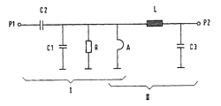
- the invention is based on the attached drawing exemplified, which is a basic circuit of the two resonant circuits shows.
- the (not shown) Transmitter / receiver electronics of the end device is connected at P1, So via a capacitor C2 with the resonant circuit I connected.
- the resonant circuit I has a parallel resistance R with which the quality of the resonant circuit is determined becomes.
- the second resonant circuit II for the low carrier frequency from e.g. 125 kHz also includes antenna A and the capacitor C3.
- the antenna A is thus two resonant circuits I and II together.
- the resonant circuit II further comprises an inductance coil L. between capacitor C3 and antenna A.
- the transmit / receive electronics is connected to the resonant circuit II at P2.
- the high or low carrier frequency for example 13.56 MHz or 125 kHz is replaced by appropriate Sinusoidal oscillators fed into the resonant circuits I and II.
Landscapes
- Engineering & Computer Science (AREA)
- Health & Medical Sciences (AREA)
- Toxicology (AREA)
- Physics & Mathematics (AREA)
- Computer Networks & Wireless Communication (AREA)
- Computer Vision & Pattern Recognition (AREA)
- General Health & Medical Sciences (AREA)
- Artificial Intelligence (AREA)
- Electromagnetism (AREA)
- General Physics & Mathematics (AREA)
- Theoretical Computer Science (AREA)
- Signal Processing (AREA)
- Near-Field Transmission Systems (AREA)
- Exchange Systems With Centralized Control (AREA)
- Insulation, Fastening Of Motor, Generator Windings (AREA)
- Polysaccharides And Polysaccharide Derivatives (AREA)
- Radar Systems Or Details Thereof (AREA)
Description
Claims (5)
- Endgerät zur Kommunikation mit berührungslos arbeitenden Datenträgern, mit einer Sende/Empfangselektronik mit zwei Schwingkreisen (I und II) mit wenigstens einem Kondensator (C1, C2) und einer gemeinsamen Antenne (A) zum Abstrahlen von elektromagnetischen Wellen, dadurch gekennzeichnet, dass ein Schwingkreis (II) für eine niedrige Trägerfrequenz und der andere Schwingkreis (I) für eine hohe Trägerfrequenz ausgelegt ist, die Sende/Empfangselektronik an den Schwingkreis (I) für die hohe Trägerfrequenz über wenigstens einen Kondensator (C2) angeschlossen ist und in dem Schwingkreis (II) für die niedrige Trägerfrequenz zwischen dem Kondensator (C3) und der Antenne (A) eine Koppel-Induktivitätsspule (L) vorgesehen ist.
- Endgerät nach Anspruch 1, dadurch gekennzeichnet, daß der Schwingkreis (I) für die hohe Trägerfrequenz wenigstens einen Parallelwiderstand (R) aufweist, mit dem die Güte des Schwingkreises eingestellt wird.
- Endgerät nach einem der vorstehenden Ansprüche, dadurch gekennzeichnet, daß das Verhältnis der hohen Trägerfrequenz zur niedrigen Trägerfrequenz wenigstens 10:1 beträgt.
- Endgerät nach einem der vorstehenden Ansprüche, dadurch gekennzeichnet, daß beide Schwingkreise (I und II) abwechselnd zur Kommunikation aktiv geschaltet sind.
- Endgerät nach einem der Ansprüche 1 bis 3, dadurch gekennzeichnet, daß beide Schwingkreise (I und II) gleichzeitig zur Kommunikation aktiv geschaltet sind.
Applications Claiming Priority (3)
| Application Number | Priority Date | Filing Date | Title |
|---|---|---|---|
| DE10002311A DE10002311C1 (de) | 2000-01-20 | 2000-01-20 | Kommunikationsendgerät |
| DE10002311 | 2000-01-20 | ||
| PCT/EP2001/000559 WO2001054049A2 (de) | 2000-01-20 | 2001-01-18 | Kommunikationsendgerät |
Publications (2)
| Publication Number | Publication Date |
|---|---|
| EP1190369A2 EP1190369A2 (de) | 2002-03-27 |
| EP1190369B1 true EP1190369B1 (de) | 2004-04-14 |
Family
ID=7628141
Family Applications (1)
| Application Number | Title | Priority Date | Filing Date |
|---|---|---|---|
| EP01909654A Expired - Lifetime EP1190369B1 (de) | 2000-01-20 | 2001-01-18 | Kommunikationsendgerät |
Country Status (9)
| Country | Link |
|---|---|
| US (1) | US6674365B2 (de) |
| EP (1) | EP1190369B1 (de) |
| JP (1) | JP2003521162A (de) |
| KR (1) | KR20020001757A (de) |
| AT (1) | ATE264525T1 (de) |
| CA (1) | CA2365205A1 (de) |
| DE (2) | DE10002311C1 (de) |
| NO (1) | NO20014445D0 (de) |
| WO (1) | WO2001054049A2 (de) |
Families Citing this family (4)
| Publication number | Priority date | Publication date | Assignee | Title |
|---|---|---|---|---|
| DE10042875C2 (de) | 2000-08-31 | 2002-12-12 | Skidata Ag | Kommunikationsendgerät |
| US7199717B2 (en) * | 2004-02-17 | 2007-04-03 | Sensormatic Electronics Corporation | Frequency-division marker for an electronic article surveillance system |
| US7164358B2 (en) * | 2004-02-17 | 2007-01-16 | Sensormatic Electronics Corporation | Frequency divider with variable capacitance |
| US7456743B2 (en) * | 2005-12-07 | 2008-11-25 | Datamars S.A. | Combined low and high frequency RFID system |
Family Cites Families (11)
| Publication number | Priority date | Publication date | Assignee | Title |
|---|---|---|---|---|
| DE3922977A1 (de) | 1989-07-12 | 1991-01-24 | Texas Instruments Deutschland | Trimmschaltung und unter verwendung einer solchen trimmschaltung ausfuehrbares abgleichverfahren |
| GB9009739D0 (en) * | 1990-05-01 | 1990-06-20 | Disys Inc | Transponder system |
| US5293137A (en) * | 1992-05-26 | 1994-03-08 | Tavis Corporation | Digital transducer system including two reactive transducers forming resonant oscillator circuits |
| NO176900C (no) * | 1992-07-31 | 1995-06-14 | Micro Design As | Framgangsmåte for individuell identifikasjon ved bruk av elektronisk interrogering, og en identifikasjonsbrikke for samme |
| US5537094A (en) * | 1995-01-27 | 1996-07-16 | Sensormatic Electronics Corporation | Method and apparatus for detecting an EAS marker using a neural network processing device |
| US5517179A (en) * | 1995-05-18 | 1996-05-14 | Xlink Enterprises, Inc. | Signal-powered frequency-dividing transponder |
| JPH09326736A (ja) * | 1996-06-03 | 1997-12-16 | Mitsubishi Electric Corp | ワイヤレス送受信システム用2次側回路装置およびワイヤレス送受信システム用誘導コイル |
| US5963173A (en) * | 1997-12-05 | 1999-10-05 | Sensormatic Electronics Corporation | Antenna and transmitter arrangement for EAS system |
| US6362738B1 (en) * | 1998-04-16 | 2002-03-26 | Motorola, Inc. | Reader for use in a radio frequency identification system and method thereof |
| DE19831767C2 (de) | 1998-07-15 | 2002-03-28 | Skidata Ag | Durchgangskontrolleinrichtung für berührungslose Datenträger |
| US6400271B1 (en) * | 2000-03-20 | 2002-06-04 | Checkpoint Systems, Inc. | Activate/deactiveable security tag with enhanced electronic protection for use with an electronic security system |
-
2000
- 2000-01-20 DE DE10002311A patent/DE10002311C1/de not_active Expired - Fee Related
-
2001
- 2001-01-18 KR KR1020017011537A patent/KR20020001757A/ko not_active Ceased
- 2001-01-18 WO PCT/EP2001/000559 patent/WO2001054049A2/de not_active Ceased
- 2001-01-18 EP EP01909654A patent/EP1190369B1/de not_active Expired - Lifetime
- 2001-01-18 JP JP2001554271A patent/JP2003521162A/ja not_active Withdrawn
- 2001-01-18 DE DE50101967T patent/DE50101967D1/de not_active Expired - Lifetime
- 2001-01-18 CA CA002365205A patent/CA2365205A1/en not_active Abandoned
- 2001-01-18 US US09/937,118 patent/US6674365B2/en not_active Expired - Lifetime
- 2001-01-18 AT AT01909654T patent/ATE264525T1/de active
- 2001-09-13 NO NO20014445A patent/NO20014445D0/no not_active Application Discontinuation
Also Published As
| Publication number | Publication date |
|---|---|
| DE50101967D1 (de) | 2004-05-19 |
| KR20020001757A (ko) | 2002-01-09 |
| WO2001054049A2 (de) | 2001-07-26 |
| EP1190369A2 (de) | 2002-03-27 |
| NO20014445L (no) | 2001-09-13 |
| CA2365205A1 (en) | 2001-07-26 |
| WO2001054049A3 (de) | 2002-01-17 |
| NO20014445D0 (no) | 2001-09-13 |
| US6674365B2 (en) | 2004-01-06 |
| JP2003521162A (ja) | 2003-07-08 |
| DE10002311C1 (de) | 2001-06-13 |
| ATE264525T1 (de) | 2004-04-15 |
| US20030071732A1 (en) | 2003-04-17 |
Similar Documents
| Publication | Publication Date | Title |
|---|---|---|
| EP1164532B1 (de) | Vorrichtung zur kontaktlosen Übertragung von Daten | |
| EP1482647B1 (de) | Schaltungsanordnung zur Phasenmodulation für rückstreubasierte Transponder | |
| DE3779723T2 (de) | Datenspeichervorrichtungen. | |
| EP0677752B1 (de) | Sensorsystem | |
| DE69323995T2 (de) | Verfahren zum Abstimmen von elektronischen Antwortgeräten | |
| DE69332198T2 (de) | Bidirektionales-Kommunikationssystem mit Doppelresonanz-Antennenschaltung für RF-Anhänger | |
| EP0826190B1 (de) | Kontaktlose chipkarte | |
| EP1336158A1 (de) | Kontaktloser datenträger | |
| DE69620658T2 (de) | Sende-Empfänger für kontaktloses IC-Kartensystem | |
| DE10393263T5 (de) | Verfahren und System für eine logarithmische Wendelantenne mit großer Bandbreite für ein Radio- frequenzidentifizierungskennzeichnungssystem | |
| EP1224607B1 (de) | Verfahren zum auslesen und beschreiben von rfid-transpondern | |
| DE10158442B4 (de) | Sende- und Empfangseinrichtung für eine kontaktlose Datenübertragung | |
| DE10325396A1 (de) | Schaltungsanordnung und Verfahren zur Phasenmodulation für rückstreubasierte Transponder | |
| DE10002311C1 (de) | Kommunikationsendgerät | |
| DE112021001455T5 (de) | Elektronische karte mit biometrischer authentifizierungsfunktion | |
| EP1756758B1 (de) | Sende-/empfangs-einrichtung | |
| DE102009019724A1 (de) | Transponder für RFID-Anwendungen sowie Verfahren zur Auslegung eines solchen Transponders | |
| EP1695454A1 (de) | Elektronisches gerät mit einem sicherheitsmodul | |
| EP1814068A1 (de) | Antenne für einen rückstreubasierten RFID-Transponder | |
| EP1323117B1 (de) | Kommunikationsendgerät | |
| DE19715215C1 (de) | Kontaktloses Transpondersystem | |
| EP2689537A1 (de) | Anlage mit einem stationären teil und einem dazu relativ bewegbar angeordneten mobilteil | |
| EP2624470B1 (de) | Elektronisches System als passiver RFID Nahfeld Transformer | |
| EP2141637A1 (de) | Tragbarer Datenträger mit aktiver Kontaktlosschnittstelle und Verfahren zum Betreiben | |
| DE10202162B4 (de) | Sicherungssystem für ein Fahrzeug mit einer Funkfrequenz-Antenne |
Legal Events
| Date | Code | Title | Description |
|---|---|---|---|
| PUAI | Public reference made under article 153(3) epc to a published international application that has entered the european phase |
Free format text: ORIGINAL CODE: 0009012 |
|
| 17P | Request for examination filed |
Effective date: 20010919 |
|
| AK | Designated contracting states |
Kind code of ref document: A2 Designated state(s): AT BE CH CY DE DK ES FI FR GB GR IE IT LI LU MC NL PT SE TR |
|
| 17Q | First examination report despatched |
Effective date: 20030312 |
|
| GRAP | Despatch of communication of intention to grant a patent |
Free format text: ORIGINAL CODE: EPIDOSNIGR1 |
|
| GRAS | Grant fee paid |
Free format text: ORIGINAL CODE: EPIDOSNIGR3 |
|
| GRAA | (expected) grant |
Free format text: ORIGINAL CODE: 0009210 |
|
| AK | Designated contracting states |
Kind code of ref document: B1 Designated state(s): AT BE CH CY DE DK ES FI FR GB GR IE IT LI LU MC NL PT SE TR |
|
| PG25 | Lapsed in a contracting state [announced via postgrant information from national office to epo] |
Ref country code: GB Free format text: LAPSE BECAUSE OF FAILURE TO SUBMIT A TRANSLATION OF THE DESCRIPTION OR TO PAY THE FEE WITHIN THE PRESCRIBED TIME-LIMIT Effective date: 20040414 Ref country code: IE Free format text: LAPSE BECAUSE OF FAILURE TO SUBMIT A TRANSLATION OF THE DESCRIPTION OR TO PAY THE FEE WITHIN THE PRESCRIBED TIME-LIMIT Effective date: 20040414 Ref country code: TR Free format text: LAPSE BECAUSE OF FAILURE TO SUBMIT A TRANSLATION OF THE DESCRIPTION OR TO PAY THE FEE WITHIN THE PRESCRIBED TIME-LIMIT Effective date: 20040414 Ref country code: FI Free format text: LAPSE BECAUSE OF FAILURE TO SUBMIT A TRANSLATION OF THE DESCRIPTION OR TO PAY THE FEE WITHIN THE PRESCRIBED TIME-LIMIT Effective date: 20040414 Ref country code: NL Free format text: LAPSE BECAUSE OF FAILURE TO SUBMIT A TRANSLATION OF THE DESCRIPTION OR TO PAY THE FEE WITHIN THE PRESCRIBED TIME-LIMIT Effective date: 20040414 |
|
| REG | Reference to a national code |
Ref country code: GB Ref legal event code: FG4D Free format text: NOT ENGLISH |
|
| REG | Reference to a national code |
Ref country code: CH Ref legal event code: EP |
|
| REF | Corresponds to: |
Ref document number: 50101967 Country of ref document: DE Date of ref document: 20040519 Kind code of ref document: P |
|
| REG | Reference to a national code |
Ref country code: IE Ref legal event code: FG4D Free format text: GERMAN |
|
| REG | Reference to a national code |
Ref country code: SE Ref legal event code: TRGR |
|
| PG25 | Lapsed in a contracting state [announced via postgrant information from national office to epo] |
Ref country code: DK Free format text: LAPSE BECAUSE OF FAILURE TO SUBMIT A TRANSLATION OF THE DESCRIPTION OR TO PAY THE FEE WITHIN THE PRESCRIBED TIME-LIMIT Effective date: 20040714 Ref country code: GR Free format text: LAPSE BECAUSE OF FAILURE TO SUBMIT A TRANSLATION OF THE DESCRIPTION OR TO PAY THE FEE WITHIN THE PRESCRIBED TIME-LIMIT Effective date: 20040714 |
|
| PG25 | Lapsed in a contracting state [announced via postgrant information from national office to epo] |
Ref country code: ES Free format text: LAPSE BECAUSE OF FAILURE TO SUBMIT A TRANSLATION OF THE DESCRIPTION OR TO PAY THE FEE WITHIN THE PRESCRIBED TIME-LIMIT Effective date: 20040725 |
|
| REG | Reference to a national code |
Ref country code: CH Ref legal event code: NV Representative=s name: KELLER & PARTNER PATENTANWAELTE AG |
|
| NLV1 | Nl: lapsed or annulled due to failure to fulfill the requirements of art. 29p and 29m of the patents act | ||
| GBV | Gb: ep patent (uk) treated as always having been void in accordance with gb section 77(7)/1977 [no translation filed] |
Effective date: 20040414 |
|
| REG | Reference to a national code |
Ref country code: IE Ref legal event code: FD4D |
|
| ET | Fr: translation filed | ||
| PG25 | Lapsed in a contracting state [announced via postgrant information from national office to epo] |
Ref country code: CY Free format text: LAPSE BECAUSE OF FAILURE TO SUBMIT A TRANSLATION OF THE DESCRIPTION OR TO PAY THE FEE WITHIN THE PRESCRIBED TIME-LIMIT Effective date: 20050118 Ref country code: LU Free format text: LAPSE BECAUSE OF NON-PAYMENT OF DUE FEES Effective date: 20050118 |
|
| PG25 | Lapsed in a contracting state [announced via postgrant information from national office to epo] |
Ref country code: BE Free format text: LAPSE BECAUSE OF NON-PAYMENT OF DUE FEES Effective date: 20050131 Ref country code: MC Free format text: LAPSE BECAUSE OF NON-PAYMENT OF DUE FEES Effective date: 20050131 |
|
| PLBE | No opposition filed within time limit |
Free format text: ORIGINAL CODE: 0009261 |
|
| STAA | Information on the status of an ep patent application or granted ep patent |
Free format text: STATUS: NO OPPOSITION FILED WITHIN TIME LIMIT |
|
| 26N | No opposition filed |
Effective date: 20050117 |
|
| BERE | Be: lapsed |
Owner name: *SKIDATA A.G. Effective date: 20050131 |
|
| BERE | Be: lapsed |
Owner name: *SKIDATA A.G. Effective date: 20050131 |
|
| PG25 | Lapsed in a contracting state [announced via postgrant information from national office to epo] |
Ref country code: PT Free format text: LAPSE BECAUSE OF NON-PAYMENT OF DUE FEES Effective date: 20040914 |
|
| PGFP | Annual fee paid to national office [announced via postgrant information from national office to epo] |
Ref country code: FR Payment date: 20110202 Year of fee payment: 11 Ref country code: DE Payment date: 20110121 Year of fee payment: 11 Ref country code: CH Payment date: 20110124 Year of fee payment: 11 Ref country code: SE Payment date: 20110113 Year of fee payment: 11 Ref country code: AT Payment date: 20110113 Year of fee payment: 11 Ref country code: IT Payment date: 20110126 Year of fee payment: 11 |
|
| REG | Reference to a national code |
Ref country code: CH Ref legal event code: PL |
|
| REG | Reference to a national code |
Ref country code: SE Ref legal event code: EUG |
|
| REG | Reference to a national code |
Ref country code: FR Ref legal event code: ST Effective date: 20120928 |
|
| PG25 | Lapsed in a contracting state [announced via postgrant information from national office to epo] |
Ref country code: CH Free format text: LAPSE BECAUSE OF NON-PAYMENT OF DUE FEES Effective date: 20120131 Ref country code: LI Free format text: LAPSE BECAUSE OF NON-PAYMENT OF DUE FEES Effective date: 20120131 Ref country code: DE Free format text: LAPSE BECAUSE OF NON-PAYMENT OF DUE FEES Effective date: 20120801 Ref country code: SE Free format text: LAPSE BECAUSE OF NON-PAYMENT OF DUE FEES Effective date: 20120119 |
|
| REG | Reference to a national code |
Ref country code: DE Ref legal event code: R119 Ref document number: 50101967 Country of ref document: DE Effective date: 20120801 |
|
| PG25 | Lapsed in a contracting state [announced via postgrant information from national office to epo] |
Ref country code: IT Free format text: LAPSE BECAUSE OF NON-PAYMENT OF DUE FEES Effective date: 20120118 |
|
| REG | Reference to a national code |
Ref country code: AT Ref legal event code: MM01 Ref document number: 264525 Country of ref document: AT Kind code of ref document: T Effective date: 20120118 |
|
| PG25 | Lapsed in a contracting state [announced via postgrant information from national office to epo] |
Ref country code: FR Free format text: LAPSE BECAUSE OF NON-PAYMENT OF DUE FEES Effective date: 20120131 |
|
| PG25 | Lapsed in a contracting state [announced via postgrant information from national office to epo] |
Ref country code: AT Free format text: LAPSE BECAUSE OF NON-PAYMENT OF DUE FEES Effective date: 20120118 |