EP1187520A2 - Electrical circuit board and a method for making the same - Google Patents
Electrical circuit board and a method for making the same Download PDFInfo
- Publication number
- EP1187520A2 EP1187520A2 EP01121380A EP01121380A EP1187520A2 EP 1187520 A2 EP1187520 A2 EP 1187520A2 EP 01121380 A EP01121380 A EP 01121380A EP 01121380 A EP01121380 A EP 01121380A EP 1187520 A2 EP1187520 A2 EP 1187520A2
- Authority
- EP
- European Patent Office
- Prior art keywords
- layer
- circuit
- conductive layer
- circuit board
- assembly
- Prior art date
- Legal status (The legal status is an assumption and is not a legal conclusion. Google has not performed a legal analysis and makes no representation as to the accuracy of the status listed.)
- Withdrawn
Links
- 238000000034 method Methods 0.000 title description 28
- 229910052751 metal Inorganic materials 0.000 claims description 11
- 239000002184 metal Substances 0.000 claims description 11
- 239000004020 conductor Substances 0.000 claims description 6
- 239000010410 layer Substances 0.000 description 76
- 239000000463 material Substances 0.000 description 26
- 239000011162 core material Substances 0.000 description 24
- 229910000679 solder Inorganic materials 0.000 description 15
- 239000000853 adhesive Substances 0.000 description 7
- 230000001070 adhesive effect Effects 0.000 description 7
- RYGMFSIKBFXOCR-UHFFFAOYSA-N Copper Chemical compound [Cu] RYGMFSIKBFXOCR-UHFFFAOYSA-N 0.000 description 5
- 229910052802 copper Inorganic materials 0.000 description 5
- 239000010949 copper Substances 0.000 description 5
- 239000003989 dielectric material Substances 0.000 description 5
- 239000004593 Epoxy Substances 0.000 description 4
- PXHVJJICTQNCMI-UHFFFAOYSA-N Nickel Chemical compound [Ni] PXHVJJICTQNCMI-UHFFFAOYSA-N 0.000 description 4
- 229910052782 aluminium Inorganic materials 0.000 description 4
- XAGFODPZIPBFFR-UHFFFAOYSA-N aluminium Chemical compound [Al] XAGFODPZIPBFFR-UHFFFAOYSA-N 0.000 description 4
- 230000000712 assembly Effects 0.000 description 4
- 238000000429 assembly Methods 0.000 description 4
- 238000005530 etching Methods 0.000 description 4
- 238000004519 manufacturing process Methods 0.000 description 3
- 150000002739 metals Chemical class 0.000 description 3
- 239000000758 substrate Substances 0.000 description 3
- XEEYBQQBJWHFJM-UHFFFAOYSA-N Iron Chemical compound [Fe] XEEYBQQBJWHFJM-UHFFFAOYSA-N 0.000 description 2
- BQCADISMDOOEFD-UHFFFAOYSA-N Silver Chemical compound [Ag] BQCADISMDOOEFD-UHFFFAOYSA-N 0.000 description 2
- 238000004891 communication Methods 0.000 description 2
- 238000007906 compression Methods 0.000 description 2
- 239000011888 foil Substances 0.000 description 2
- PCHJSUWPFVWCPO-UHFFFAOYSA-N gold Chemical compound [Au] PCHJSUWPFVWCPO-UHFFFAOYSA-N 0.000 description 2
- 229910052737 gold Inorganic materials 0.000 description 2
- 239000010931 gold Substances 0.000 description 2
- 238000010030 laminating Methods 0.000 description 2
- 238000003754 machining Methods 0.000 description 2
- 229910052759 nickel Inorganic materials 0.000 description 2
- 229910052709 silver Inorganic materials 0.000 description 2
- 239000004332 silver Substances 0.000 description 2
- ATJFFYVFTNAWJD-UHFFFAOYSA-N Tin Chemical compound [Sn] ATJFFYVFTNAWJD-UHFFFAOYSA-N 0.000 description 1
- 229910045601 alloy Inorganic materials 0.000 description 1
- 239000000956 alloy Substances 0.000 description 1
- 238000005452 bending Methods 0.000 description 1
- 239000011248 coating agent Substances 0.000 description 1
- 238000000576 coating method Methods 0.000 description 1
- 230000006835 compression Effects 0.000 description 1
- 238000010276 construction Methods 0.000 description 1
- 239000012792 core layer Substances 0.000 description 1
- 230000002950 deficient Effects 0.000 description 1
- 238000005553 drilling Methods 0.000 description 1
- 239000012530 fluid Substances 0.000 description 1
- 238000007654 immersion Methods 0.000 description 1
- 229910052742 iron Inorganic materials 0.000 description 1
- 230000007257 malfunction Effects 0.000 description 1
- 238000010297 mechanical methods and process Methods 0.000 description 1
- 230000005226 mechanical processes and functions Effects 0.000 description 1
- 238000001465 metallisation Methods 0.000 description 1
- 238000007747 plating Methods 0.000 description 1
- 238000007639 printing Methods 0.000 description 1
- 238000005476 soldering Methods 0.000 description 1
- 239000011135 tin Substances 0.000 description 1
- 229910052718 tin Inorganic materials 0.000 description 1
Images


Classifications
-
- H—ELECTRICITY
- H05—ELECTRIC TECHNIQUES NOT OTHERWISE PROVIDED FOR
- H05K—PRINTED CIRCUITS; CASINGS OR CONSTRUCTIONAL DETAILS OF ELECTRIC APPARATUS; MANUFACTURE OF ASSEMBLAGES OF ELECTRICAL COMPONENTS
- H05K3/00—Apparatus or processes for manufacturing printed circuits
- H05K3/40—Forming printed elements for providing electric connections to or between printed circuits
- H05K3/4038—Through-connections; Vertical interconnect access [VIA] connections
- H05K3/4084—Through-connections; Vertical interconnect access [VIA] connections by deforming at least one of the conductive layers
-
- H—ELECTRICITY
- H05—ELECTRIC TECHNIQUES NOT OTHERWISE PROVIDED FOR
- H05K—PRINTED CIRCUITS; CASINGS OR CONSTRUCTIONAL DETAILS OF ELECTRIC APPARATUS; MANUFACTURE OF ASSEMBLAGES OF ELECTRICAL COMPONENTS
- H05K1/00—Printed circuits
- H05K1/02—Details
- H05K1/03—Use of materials for the substrate
- H05K1/05—Insulated conductive substrates, e.g. insulated metal substrate
- H05K1/056—Insulated conductive substrates, e.g. insulated metal substrate the metal substrate being covered by an organic insulating layer
-
- H—ELECTRICITY
- H05—ELECTRIC TECHNIQUES NOT OTHERWISE PROVIDED FOR
- H05K—PRINTED CIRCUITS; CASINGS OR CONSTRUCTIONAL DETAILS OF ELECTRIC APPARATUS; MANUFACTURE OF ASSEMBLAGES OF ELECTRICAL COMPONENTS
- H05K2201/00—Indexing scheme relating to printed circuits covered by H05K1/00
- H05K2201/03—Conductive materials
- H05K2201/0302—Properties and characteristics in general
- H05K2201/0305—Solder used for other purposes than connections between PCB or components, e.g. for filling vias or for programmable patterns
-
- H—ELECTRICITY
- H05—ELECTRIC TECHNIQUES NOT OTHERWISE PROVIDED FOR
- H05K—PRINTED CIRCUITS; CASINGS OR CONSTRUCTIONAL DETAILS OF ELECTRIC APPARATUS; MANUFACTURE OF ASSEMBLAGES OF ELECTRICAL COMPONENTS
- H05K2201/00—Indexing scheme relating to printed circuits covered by H05K1/00
- H05K2201/03—Conductive materials
- H05K2201/0332—Structure of the conductor
- H05K2201/0335—Layered conductors or foils
- H05K2201/0361—Etched tri-metal structure, i.e. metal layers or metal patterns on both sides of a different central metal layer which is later at least partly etched
-
- H—ELECTRICITY
- H05—ELECTRIC TECHNIQUES NOT OTHERWISE PROVIDED FOR
- H05K—PRINTED CIRCUITS; CASINGS OR CONSTRUCTIONAL DETAILS OF ELECTRIC APPARATUS; MANUFACTURE OF ASSEMBLAGES OF ELECTRICAL COMPONENTS
- H05K2201/00—Indexing scheme relating to printed circuits covered by H05K1/00
- H05K2201/03—Conductive materials
- H05K2201/0332—Structure of the conductor
- H05K2201/0364—Conductor shape
- H05K2201/0379—Stacked conductors
-
- H—ELECTRICITY
- H05—ELECTRIC TECHNIQUES NOT OTHERWISE PROVIDED FOR
- H05K—PRINTED CIRCUITS; CASINGS OR CONSTRUCTIONAL DETAILS OF ELECTRIC APPARATUS; MANUFACTURE OF ASSEMBLAGES OF ELECTRICAL COMPONENTS
- H05K2201/00—Indexing scheme relating to printed circuits covered by H05K1/00
- H05K2201/03—Conductive materials
- H05K2201/0332—Structure of the conductor
- H05K2201/0388—Other aspects of conductors
- H05K2201/0397—Tab
-
- H—ELECTRICITY
- H05—ELECTRIC TECHNIQUES NOT OTHERWISE PROVIDED FOR
- H05K—PRINTED CIRCUITS; CASINGS OR CONSTRUCTIONAL DETAILS OF ELECTRIC APPARATUS; MANUFACTURE OF ASSEMBLAGES OF ELECTRICAL COMPONENTS
- H05K2201/00—Indexing scheme relating to printed circuits covered by H05K1/00
- H05K2201/09—Shape and layout
- H05K2201/09209—Shape and layout details of conductors
- H05K2201/095—Conductive through-holes or vias
- H05K2201/09554—Via connected to metal substrate
-
- H—ELECTRICITY
- H05—ELECTRIC TECHNIQUES NOT OTHERWISE PROVIDED FOR
- H05K—PRINTED CIRCUITS; CASINGS OR CONSTRUCTIONAL DETAILS OF ELECTRIC APPARATUS; MANUFACTURE OF ASSEMBLAGES OF ELECTRICAL COMPONENTS
- H05K2203/00—Indexing scheme relating to apparatus or processes for manufacturing printed circuits covered by H05K3/00
- H05K2203/01—Tools for processing; Objects used during processing
- H05K2203/0195—Tool for a process not provided for in H05K3/00, e.g. tool for handling objects using suction, for deforming objects, for applying local pressure
-
- H—ELECTRICITY
- H05—ELECTRIC TECHNIQUES NOT OTHERWISE PROVIDED FOR
- H05K—PRINTED CIRCUITS; CASINGS OR CONSTRUCTIONAL DETAILS OF ELECTRIC APPARATUS; MANUFACTURE OF ASSEMBLAGES OF ELECTRICAL COMPONENTS
- H05K2203/00—Indexing scheme relating to apparatus or processes for manufacturing printed circuits covered by H05K3/00
- H05K2203/06—Lamination
- H05K2203/063—Lamination of preperforated insulating layer
-
- H—ELECTRICITY
- H05—ELECTRIC TECHNIQUES NOT OTHERWISE PROVIDED FOR
- H05K—PRINTED CIRCUITS; CASINGS OR CONSTRUCTIONAL DETAILS OF ELECTRIC APPARATUS; MANUFACTURE OF ASSEMBLAGES OF ELECTRICAL COMPONENTS
- H05K3/00—Apparatus or processes for manufacturing printed circuits
- H05K3/02—Apparatus or processes for manufacturing printed circuits in which the conductive material is applied to the surface of the insulating support and is thereafter removed from such areas of the surface which are not intended for current conducting or shielding
- H05K3/06—Apparatus or processes for manufacturing printed circuits in which the conductive material is applied to the surface of the insulating support and is thereafter removed from such areas of the surface which are not intended for current conducting or shielding the conductive material being removed chemically or electrolytically, e.g. by photo-etch process
- H05K3/061—Etching masks
- H05K3/062—Etching masks consisting of metals or alloys or metallic inorganic compounds
-
- H—ELECTRICITY
- H05—ELECTRIC TECHNIQUES NOT OTHERWISE PROVIDED FOR
- H05K—PRINTED CIRCUITS; CASINGS OR CONSTRUCTIONAL DETAILS OF ELECTRIC APPARATUS; MANUFACTURE OF ASSEMBLAGES OF ELECTRICAL COMPONENTS
- H05K3/00—Apparatus or processes for manufacturing printed circuits
- H05K3/40—Forming printed elements for providing electric connections to or between printed circuits
- H05K3/4092—Integral conductive tabs, i.e. conductive parts partly detached from the substrate
-
- H—ELECTRICITY
- H05—ELECTRIC TECHNIQUES NOT OTHERWISE PROVIDED FOR
- H05K—PRINTED CIRCUITS; CASINGS OR CONSTRUCTIONAL DETAILS OF ELECTRIC APPARATUS; MANUFACTURE OF ASSEMBLAGES OF ELECTRICAL COMPONENTS
- H05K3/00—Apparatus or processes for manufacturing printed circuits
- H05K3/44—Manufacturing insulated metal core circuits or other insulated electrically conductive core circuits
-
- H—ELECTRICITY
- H05—ELECTRIC TECHNIQUES NOT OTHERWISE PROVIDED FOR
- H05K—PRINTED CIRCUITS; CASINGS OR CONSTRUCTIONAL DETAILS OF ELECTRIC APPARATUS; MANUFACTURE OF ASSEMBLAGES OF ELECTRICAL COMPONENTS
- H05K3/00—Apparatus or processes for manufacturing printed circuits
- H05K3/44—Manufacturing insulated metal core circuits or other insulated electrically conductive core circuits
- H05K3/445—Manufacturing insulated metal core circuits or other insulated electrically conductive core circuits having insulated holes or insulated via connections through the metal core
-
- Y—GENERAL TAGGING OF NEW TECHNOLOGICAL DEVELOPMENTS; GENERAL TAGGING OF CROSS-SECTIONAL TECHNOLOGIES SPANNING OVER SEVERAL SECTIONS OF THE IPC; TECHNICAL SUBJECTS COVERED BY FORMER USPC CROSS-REFERENCE ART COLLECTIONS [XRACs] AND DIGESTS
- Y10—TECHNICAL SUBJECTS COVERED BY FORMER USPC
- Y10T—TECHNICAL SUBJECTS COVERED BY FORMER US CLASSIFICATION
- Y10T29/00—Metal working
- Y10T29/49—Method of mechanical manufacture
- Y10T29/49002—Electrical device making
- Y10T29/49117—Conductor or circuit manufacturing
- Y10T29/49124—On flat or curved insulated base, e.g., printed circuit, etc.
- Y10T29/49128—Assembling formed circuit to base
-
- Y—GENERAL TAGGING OF NEW TECHNOLOGICAL DEVELOPMENTS; GENERAL TAGGING OF CROSS-SECTIONAL TECHNOLOGIES SPANNING OVER SEVERAL SECTIONS OF THE IPC; TECHNICAL SUBJECTS COVERED BY FORMER USPC CROSS-REFERENCE ART COLLECTIONS [XRACs] AND DIGESTS
- Y10—TECHNICAL SUBJECTS COVERED BY FORMER USPC
- Y10T—TECHNICAL SUBJECTS COVERED BY FORMER US CLASSIFICATION
- Y10T29/00—Metal working
- Y10T29/49—Method of mechanical manufacture
- Y10T29/49002—Electrical device making
- Y10T29/49117—Conductor or circuit manufacturing
- Y10T29/49124—On flat or curved insulated base, e.g., printed circuit, etc.
- Y10T29/4913—Assembling to base an electrical component, e.g., capacitor, etc.
- Y10T29/49144—Assembling to base an electrical component, e.g., capacitor, etc. by metal fusion
-
- Y—GENERAL TAGGING OF NEW TECHNOLOGICAL DEVELOPMENTS; GENERAL TAGGING OF CROSS-SECTIONAL TECHNOLOGIES SPANNING OVER SEVERAL SECTIONS OF THE IPC; TECHNICAL SUBJECTS COVERED BY FORMER USPC CROSS-REFERENCE ART COLLECTIONS [XRACs] AND DIGESTS
- Y10—TECHNICAL SUBJECTS COVERED BY FORMER USPC
- Y10T—TECHNICAL SUBJECTS COVERED BY FORMER US CLASSIFICATION
- Y10T29/00—Metal working
- Y10T29/49—Method of mechanical manufacture
- Y10T29/49002—Electrical device making
- Y10T29/49117—Conductor or circuit manufacturing
- Y10T29/49124—On flat or curved insulated base, e.g., printed circuit, etc.
- Y10T29/49155—Manufacturing circuit on or in base
- Y10T29/49156—Manufacturing circuit on or in base with selective destruction of conductive paths
Definitions
- the present invention relates to an electrical circuit board and more particularly, to a multi-layer electrical circuit board having interconnections between portions or layers of the circuit board.
- Multi-layer circuit boards contain and/or include electrical components which selectively and operatively populate opposed first and second surfaces (i.e., top and bottom surfaces) of each board (or other respective interior portions of each of the boards), thereby desirably allowing each of the electrical circuit boards to contain and/or include a relatively large amount of electrical components which efficiently and densely populate the respective boards.
- This communication and interconnection may require the use of shared electrical ground planes, the transmittal of electrical power and/or control type signals between each of the component containing surfaces and/or the component containing board portions, and/or the selective and physical connection of various contained components.
- This desired interconnection typically requires one or more vias, apertures and/or holes to be drilled, etched and/or formed through the core of the circuit board substrate, thereby selectively creating one or more vias, apertures and/or holes which pass through and/or traverse some or all of the component containing surfaces and/or layers of the circuit board.
- the vias are then typically filled with solder (e.g., a pin or component connector is soldered into the hole).
- solder e.g., a pin or component connector is soldered into the hole.
- a method for forming a connection within a multi-layer circuit board includes a core member having a top surface and a bottom surface, and first and second conductive members, which are respectively attached to the top and the bottom surface of the core member.
- the method includes the steps of: selectively removing a portion of the core member, effective to cause a portion of the first conductive member to form an air bridge over the second conductive member; providing a bonding tool; imparting a force upon the air bridge by use of the bonding tool, the force being effective to collapse a portion of the air bridge; and bonding the collapsed portion of the air bridge to the second conductive member, thereby connecting the first conductive member to the second conductive member.
- a multi-layer circuit board assembly includes a first circuit portion having a top surface and a bottom surface; a first pre-circuit assembly which is attached to the top surface of the first circuit portion and which includes a top conductive layer; a second pre-circuit assembly which is attached to the bottom surface of the first circuit portion and which includes a bottom conductive layer; an aperture which is formed through the first circuit portion, the first pre-circuit assembly and the second pre-circuit assembly; and a plurality of tab portions which are integrally formed from the top conductive layer, which extend through the aperture and which are coupled to the bottom conductive layer, thereby connecting the top conductive layer to the bottom conductive layer.
- Circuit assembly 10 is formed by "building up” or sequentially adding various layers of certain materials to a core or ground member or layer 12, in a conventional manner.
- Core member 12 is manufactured and/or formed from an electrically conductive material such as copper or a metallic and electrically conductive foil material.
- a pair of substantially identical layers of dielectric material or conventional epoxy 14 are respectively applied/coupled to and substantially “cover” the "top” and “bottom” surfaces of member 12.
- Two layers of a conventional adhesive material 16 are applied/coupled to and substantially “cover” or coat the respective "outer” surface of each epoxy layer 14.
- Circuit assembly 10 further includes a pair of pre-circuit assemblies 24, 32.
- Each pre-circuit assembly 24, 32 respectively includes a core metal portion or layer 20, 28 which is preferably manufactured and/or formed from a conventional aluminum material, and a pair of electrically conductive layers 18, 22 and 26, 30 which are respectively attached to the opposing surfaces (e.g., top and bottom surfaces) of core metal portions 20, 28.
- the electrically conductive layers 18 are preferably manufactured and/or formed from a conventional copper material. While copper and aluminum are used to form circuit board 10 in the preferred embodiment of the invention, it should be appreciated that other metals and metal combinations can be used to form circuit board 10 and all of the other circuit boards described herein, and may include metals such as iron, nickel, silver, gold, tin and alloys thereof.
- Adhesive materials or layers 16 are disposed between each dielectric layer 14 and each pre-circuit assembly 24, 32 and respectively and operatively bond the conductive layers 18, 26 of each pre-circuit assembly 24, 32 to each dielectric layer 14.
- pre-circuit assemblies 24, 32 and/or electrically conductive members 18, 26 are connected, coupled, and/or attached to adhesive material 16 by use of a known and conventional laminating process such as a conventional "one-step" laminating process.
- portions of pre-circuit assembly 24, adhesive material 16, and dielectric layer 14 are selectively removed from the circuit assembly 10, as shown in Figure 1(b).
- portions of adhesive material 16 and dielectric material 14 are first selectively removed from an area or region 38 of the circuit assembly 10 in a conventional manner (e.g., by routing or machining).
- Portions of layers 22, 20 and 18 are then selectively removed from region 38 and from a region 34 by use of a conventional differential etching process or technique.
- the afore-described material removal or etching process is effective to create and/or form "air bridges" or crossover members 36 and 40.
- a portion or “strip” of conductive member or layer 22 forms a "bridge" 36 which is disposed over a portion of conductive member or layer 18, and a portion or “strip” of conductive member or layer 18 forms a "bridge” 40 over a portion of core 12.
- portions of the aluminum layer 20 remain attached to the bridges 36, 40 and assist in the below described bonding process.
- portions of layers 22, 20 and 18 are selectively removed prior to the assembly of circuit board 10.
- bridges 36, 40 are metallized by use of a conventional plating process (e.g., an immersion process).
- bridges 36, 40 are metallized with a conductive metal such as silver, gold or nickel, or combination of these and other metals, thereby increasing the overall "conductivity" of the bridges 36, 40 and/or increasing the amount of charge or current that the bridges 36, 40 can effectively carry or transfer.
- the metalization of the bridges 36, 40 of the preferred embodiment additionally provide a metallurgically bondable surface finish for bonding or soldering.
- a conventional metallurgical bonding tool 42 (e.g., an ultrasonic or thermo-compression bonding tool) having a relatively sharp edge 44 is positioned over bridges 36, 40.
- the bridges 36, 40 may be etched with stress concentration features, such as notches, or the bridges may be etched through so that the bridge is severed prior to being joined.
- the bonding tool 42 is moved downward in the direction of arrow 46 from the position illustrated in Figure 1(c) to the position illustrated in Figure 1(d).
- bonding tool 42 contacts air bridges 36 and 40 and is effective to "sever” or “collapse” the air bridges 36, 40, thereby respectively forming interconnection apertures or vias 52, 54. Additionally, the downward force applied to the severed ends 48, 50, by the bonding tool 42 causes the severed ends 48, 50 to respectively and forcibly contact conductive layer 18 and core 12. This forms a reliable interconnection between conductive layers 22 and 18, and between conductive layers 18 and 12. In other alternate embodiments, other types of bonding tools, methods and/or devices may be used to collapse air bridges 36, 40 and to bond members 22 and 18 and members 18 and 12.
- an amount of solder or conductive material 56 is selectively inserted into the formed aperture or via 52 after the layers 22 and 18 have been either ultrasonically bonded or simply formed into place.
- the conductive material 56 is effective to provide a more robust and reliable connection between layers 22 and 18.
- an amount of solder or conductive material 58 is selectively inserted into formed aperture or via 54 after layers 18 and 12 are bonded.
- Solder material 58 is effective to further interconnect layer 22 with layers 18 and 12 and to provide more robust and reliable interconnections between layers 22, 18 and 12.
- solder material 56 and 58 is selectively inserted or deposited into vias 52 and 54 in a molten state.
- solder material 56 and 58 is selectively inserted or deposited into vias 52 and 54 by use of a conventional compression printing technique.
- Circuit assembly 60 is formed by "building up” or sequentially adding various layers of certain materials to a core or ground member or layer 62, in a conventional manner.
- Core member 62 is manufactured and/or formed from an electrically conductive material such as copper or a metallic and electrically conductive foil material.
- a pair of substantially identical layers of dielectric material or conventional epoxy 64 are respectively applied/coupled to and substantially “cover” the "top” and “bottom” surfaces of core member 62.
- Conventional adhesive material is preferably applied/coupled to and substantially “covers” or coats the respective "outer” surfaces of each epoxy layer 64, and is effective to bond layers 68 and 80 to layer 64.
- Circuit assembly 60 further includes a pair of pre-circuit assemblies 66, 74.
- Each pre-circuit assembly 66, 74 respectively includes a core metal portion 70, 78 which is preferably manufactured and/or formed from a conventional aluminum material, and a pair of electrically conductive layers 68, 72 and 76, 80 which are respectively attached to the opposing surfaces of core metal portions 70, 78.
- the electrically conductive layers 68, 72 and 76, 80 are preferably manufactured and/or formed from a conventional copper material.
- Each pre-circuit assembly 66, 74 is respectively and operatively attached/coupled to each dielectric layer 64 by use of the conventional adhesive material.
- Circuit assembly 60 further includes a solder mask material 82 which is conventionally applied/coupled to portions of dielectric layer 64 and to conductive layer or member 72.
- the solder mask may also be applied to the bottom side of the substrate surfaces (i.e., 64 and 76).
- certain portions of pre-circuit assemblies 66, 74, dielectric material 64, and core 62 are selectively removed from a region 84 of the circuit assembly 60, as shown in Figure 2(a).
- portions of layers 76 - 80, 68, 70 and 62 are selectively removed from region 84 by use of a conventional etching process, procedure or technique
- portions of dielectric material 64 are selectively removed from region 84 by use of a conventional mechanical process (e.g., by routing, drilling, or machining), thereby forming a cavity or via 86.
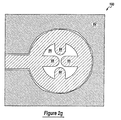
- Region 84 and via 86 are preferably generally circular in shape.
- Core layer 62 is preferably further "recessed" (e.g., etched) back from via 86 in order to prevent traces 88 from being shorted (e.g., connected to layer 62). In other alternate embodiments, core 62 is not recessed in order to intentionally short or connect traces 88 to core 62.
- protrusions or extensions 88 are forced downward in the direction illustrated by arrow 90, and move from the position shown in Figure 2(a) to the position shown in Figure 2(b).
- portions 88 are forced and/or moved downward by use of air pressure, fluid pressure, mechanical force, or a lead forming device. It should be appreciated that once protrusions 88 have been forced downward into the position illustrated in Figure 2(b), protrusions 88 each contact conductive layers or members 68, 80, and 76, and create a physical and electrical interconnection between members 76, 80, 68 and 72.
- End portions 92 are then "bent” or folded over portions or members 76 as illustrated in Figure 2(c), thereby securing protrusions 88 in an operatively “connected” position (e.g., protrusions 88 operatively connect members 76, 80, 68 and 72).
- solder paste 94 is conventionally dispensed and/or inserted within aperture 86, as illustrated in Figure 2(d).
- a conventional solder paste dispensing syringe is inserted into aperture 86 prior to the deformation or "bending" of protrusions 88, and is effective to deform and/or force protrusions 88 downward (e.g., into the position illustrated in Figure 2(b)) when the syringe is inserted.
- the syringe As the syringe is removed, it disposes, dispenses and/or deposits solder paste or material 94 within the aperture or via 86.
- circuit assembly 60 allows the "non-wettable" insulating layers or members 64 (i.e., layers or members 64 cannot be metallurgically bonded to conventional solder material) to be initially “bridged” or crossed-over, effective to connect members 68, 72, 76, and 80, without the use of solder material.
- Circuit assembly 100 is substantially identical in structure and function to circuit assembly 60 with the exception that a total of four protrusions 88 are formed and/or utilized instead of two protrusions 88. In this manner, circuit assembly 100 provides a more robust and reliable connection between conducting members or layers 68, 72, 76, and 80.
- the dielectric insulative or "solder mask" material 101 can be applied to the via walls of the core 62 to prevent any shorting of traces 88 to core 62, as opposed to the technique used in Figures 2(a)-2(e) where the recessing of the core material 62 prevents shorting. If shorting of the trace 88 to the core 62 is desired then no recessing or coating of core material 62 is used.
Landscapes
- Engineering & Computer Science (AREA)
- Manufacturing & Machinery (AREA)
- Microelectronics & Electronic Packaging (AREA)
- Production Of Multi-Layered Print Wiring Board (AREA)
- Printing Elements For Providing Electric Connections Between Printed Circuits (AREA)
Abstract
Description
Claims (5)
- A multi-layer circuit board assembly comprising:a first circuit portion having a top surface and a bottom surface;a first pre-circuit assembly which is attached to said top surface of said first circuit portion and which includes a top conductive layer;a second pre-circuit assembly which is attached to said bottom surface of said first circuit portion and which includes a bottom conductive layer;an aperture which is formed through said first circuit portion, said first pre-circuit assembly and said second pre-circuit assembly; anda plurality of tab portions which are integrally formed from said top conductive layer, which extend through said aperture and which are coupled to said bottom conductive layer, thereby connecting said top conductive layer to said bottom conductive layer.
- The multi-layer circuit board assembly of claim 1 wherein said first pre-circuit assembly further includes a second conductive layer and a first core metal layer which is disposed between said second conductive layer and said top conductive layer, and wherein said plurality of tab members are further effective to connect said second conductive layer to said top and bottom conductive layers.
- The multi-layer circuit board assembly of claim 2 wherein said second pre-circuit assembly further includes a third conductive layer and a second core metal layer which is disposed between said third conductive layer and said bottom conductive layer, and wherein said plurality of tab members are further effective to connect said third conductive layer to said second conductive layer and said top and bottom conductive layers.
- The multi-layer circuit board assembly of claim 1 wherein said first circuit portion comprises a conductive core member having a first and second surface and a pair of dielectric members which are attached to said first and second surfaces.
- The multi-layer circuit board assembly of claim 1 further comprising an amount of conductive material which is disposed within said aperture.
Applications Claiming Priority (2)
| Application Number | Priority Date | Filing Date | Title |
|---|---|---|---|
| US655986 | 2000-09-06 | ||
| US09/655,986 US6449839B1 (en) | 2000-09-06 | 2000-09-06 | Electrical circuit board and a method for making the same |
Publications (2)
| Publication Number | Publication Date |
|---|---|
| EP1187520A2 true EP1187520A2 (en) | 2002-03-13 |
| EP1187520A3 EP1187520A3 (en) | 2003-01-15 |
Family
ID=24631182
Family Applications (1)
| Application Number | Title | Priority Date | Filing Date |
|---|---|---|---|
| EP01121380A Withdrawn EP1187520A3 (en) | 2000-09-06 | 2001-09-06 | Electrical circuit board and a method for making the same |
Country Status (3)
| Country | Link |
|---|---|
| US (1) | US6449839B1 (en) |
| EP (1) | EP1187520A3 (en) |
| JP (1) | JP2002124770A (en) |
Cited By (2)
| Publication number | Priority date | Publication date | Assignee | Title |
|---|---|---|---|---|
| CN102791446A (en) * | 2010-03-15 | 2012-11-21 | 吉列公司 | Razor cartridges |
| DE102009032998B4 (en) * | 2008-07-14 | 2015-05-28 | Infineon Technologies Ag | Component with contact elements and method for producing the same |
Families Citing this family (3)
| Publication number | Priority date | Publication date | Assignee | Title |
|---|---|---|---|---|
| US7152315B1 (en) * | 2001-03-20 | 2006-12-26 | Visteon Global Technologies, Inc. | Method of making a printed circuit board |
| DE102005033218A1 (en) * | 2005-07-15 | 2007-01-18 | Printed Systems Gmbh | Three-dimensional circuit |
| WO2022113779A1 (en) * | 2020-11-30 | 2022-06-02 | 株式会社村田製作所 | Laminated substrate, and manufacturing method for laminated substrate |
Family Cites Families (21)
| Publication number | Priority date | Publication date | Assignee | Title |
|---|---|---|---|---|
| JPS5146904B2 (en) | 1971-09-30 | 1976-12-11 | ||
| US3977074A (en) * | 1975-02-06 | 1976-08-31 | General Motors Corporation | Double sided printed circuit board and method for making same |
| US4319708A (en) * | 1977-02-15 | 1982-03-16 | Lomerson Robert B | Mechanical bonding of surface conductive layers |
| NL181611C (en) * | 1978-11-14 | 1987-09-16 | Philips Nv | METHOD FOR MANUFACTURING A WIRING SYSTEM, AND A SEMICONDUCTOR DEVICE EQUIPPED WITH SUCH WIRING SYSTEM. |
| US4289846A (en) * | 1979-12-28 | 1981-09-15 | General Electric Company | Process for forming low-reactance interconnections on semiconductors |
| US4404059A (en) | 1982-05-26 | 1983-09-13 | Livshits Vladimir I | Process for manufacturing panels to be used in microelectronic systems |
| JPH01173694A (en) * | 1987-12-26 | 1989-07-10 | Shindo Denshi Kogyo Kk | Manufacture of double-faced through-hole film carrier |
| JP3019884B2 (en) * | 1991-09-05 | 2000-03-13 | 松下電器産業株式会社 | Semiconductor device and manufacturing method thereof |
| US5408742A (en) * | 1991-10-28 | 1995-04-25 | Martin Marietta Corporation | Process for making air bridges for integrated circuits |
| CA2114792A1 (en) * | 1992-06-15 | 1993-12-16 | Walter Schmidt | Process for producing subsequently conditionable contact points on circuit substrates and circuit substrates with such contact points |
| US5658698A (en) * | 1994-01-31 | 1997-08-19 | Canon Kabushiki Kaisha | Microstructure, process for manufacturing thereof and devices incorporating the same |
| TW308719B (en) * | 1995-10-23 | 1997-06-21 | Dow Corning | |
| US5738797A (en) | 1996-05-17 | 1998-04-14 | Ford Global Technologies, Inc. | Three-dimensional multi-layer circuit structure and method for forming the same |
| US5976391A (en) * | 1998-01-13 | 1999-11-02 | Ford Motor Company | Continuous Flexible chemically-milled circuit assembly with multiple conductor layers and method of making same |
| JP3111977B2 (en) * | 1998-05-15 | 2000-11-27 | 日本電気株式会社 | Method for manufacturing semiconductor device |
| US6248247B1 (en) * | 1998-12-01 | 2001-06-19 | Visteon Global Technologies, Inc. | Method of fortifying an air bridge circuit |
| US6217783B1 (en) * | 1998-12-01 | 2001-04-17 | Visteon Global Technologies, Inc. | Method for strengthening air bridge circuits |
| US6218282B1 (en) * | 1999-02-18 | 2001-04-17 | Advanced Micro Devices, Inc. | Method of forming low dielectric tungsten lined interconnection system |
| US6214719B1 (en) * | 1999-09-30 | 2001-04-10 | Novellus Systems, Inc. | Method of implementing air-gap technology for low capacitance ILD in the damascene scheme |
| US6265321B1 (en) * | 2000-04-17 | 2001-07-24 | Chartered Semiconductor Manufacturing Ltd. | Air bridge process for forming air gaps |
| US6287979B1 (en) * | 2000-04-17 | 2001-09-11 | Chartered Semiconductor Manufacturing Ltd. | Method for forming an air gap as low dielectric constant material using buckminsterfullerene as a porogen in an air bridge or a sacrificial layer |
-
2000
- 2000-09-06 US US09/655,986 patent/US6449839B1/en not_active Expired - Fee Related
-
2001
- 2001-09-06 EP EP01121380A patent/EP1187520A3/en not_active Withdrawn
- 2001-09-06 JP JP2001270253A patent/JP2002124770A/en active Pending
Cited By (3)
| Publication number | Priority date | Publication date | Assignee | Title |
|---|---|---|---|---|
| DE102009032998B4 (en) * | 2008-07-14 | 2015-05-28 | Infineon Technologies Ag | Component with contact elements and method for producing the same |
| CN102791446A (en) * | 2010-03-15 | 2012-11-21 | 吉列公司 | Razor cartridges |
| CN102791446B (en) * | 2010-03-15 | 2014-12-31 | 吉列公司 | Razor cartridges |
Also Published As
| Publication number | Publication date |
|---|---|
| EP1187520A3 (en) | 2003-01-15 |
| US6449839B1 (en) | 2002-09-17 |
| JP2002124770A (en) | 2002-04-26 |
Similar Documents
| Publication | Publication Date | Title |
|---|---|---|
| US5962815A (en) | Antifuse interconnect between two conducting layers of a printed circuit board | |
| JP3492348B2 (en) | Method of manufacturing package for semiconductor device | |
| US20100071944A1 (en) | Chip capacitor embedded pwb | |
| JP2000332369A (en) | Printed circuit board and manufacturing method thereof | |
| KR19990035858A (en) | Method for forming protruding metal contacts for permanent engagement on electrical circuits | |
| US6998540B2 (en) | Electrical circuit board and a method for making the same | |
| KR100315588B1 (en) | Manufacturing method of multilayer wiring board | |
| US6495053B1 (en) | Electrical circuit board and a method for making the same | |
| US6449839B1 (en) | Electrical circuit board and a method for making the same | |
| US7218530B2 (en) | Enhanced blind hole termination of pin to PCB | |
| TWI295912B (en) | Method for manufacturing a substrate embedded with an electronic component and device from the same | |
| JP4635331B2 (en) | Printed wiring board | |
| US7083901B2 (en) | Joining member for Z-interconnect in electronic devices without conductive paste | |
| US7124503B1 (en) | Method for forming multilayer circuit board | |
| EP1187519B1 (en) | Electrical circuit board and a method for making the same | |
| JP2002198628A (en) | Printed circuit board and manufacturing method thereof | |
| US6391211B1 (en) | Method for making an electrical circuit board | |
| KR100821596B1 (en) | Semiconductor device using multilayer wiring board and multilayer wiring board | |
| US7152315B1 (en) | Method of making a printed circuit board | |
| US6739041B2 (en) | Circuit board and a method for making the same | |
| JP2002016330A (en) | Component mounting board and method of manufacturing the same | |
| JP2006303338A (en) | Multilayer circuit board and manufacturing method thereof | |
| JP2000013022A (en) | Multilayer wiring circuit board and method of manufacturing the same | |
| US6412168B1 (en) | Method of making an electrical circuit board | |
| US6673723B2 (en) | Circuit board and a method for making the same |
Legal Events
| Date | Code | Title | Description |
|---|---|---|---|
| PUAI | Public reference made under article 153(3) epc to a published international application that has entered the european phase |
Free format text: ORIGINAL CODE: 0009012 |
|
| AK | Designated contracting states |
Kind code of ref document: A2 Designated state(s): AT BE CH CY DE DK ES FI FR GB GR IE IT LI LU MC NL PT SE TR |
|
| AX | Request for extension of the european patent |
Free format text: AL;LT;LV;MK;RO;SI |
|
| 17P | Request for examination filed |
Effective date: 20020813 |
|
| PUAL | Search report despatched |
Free format text: ORIGINAL CODE: 0009013 |
|
| AK | Designated contracting states |
Kind code of ref document: A3 Designated state(s): AT BE CH CY DE DK ES FI FR GB GR IE IT LI LU MC NL PT SE TR |
|
| AX | Request for extension of the european patent |
Free format text: AL;LT;LV;MK;RO;SI |
|
| AKX | Designation fees paid |
Designated state(s): DE ES FR GB PT SE |
|
| 17Q | First examination report despatched |
Effective date: 20031009 |
|
| STAA | Information on the status of an ep patent application or granted ep patent |
Free format text: STATUS: THE APPLICATION IS DEEMED TO BE WITHDRAWN |
|
| 18D | Application deemed to be withdrawn |
Effective date: 20050106 |