EP1187325A2 - Multilayer type piezoelectric filter - Google Patents
Multilayer type piezoelectric filter Download PDFInfo
- Publication number
- EP1187325A2 EP1187325A2 EP01120910A EP01120910A EP1187325A2 EP 1187325 A2 EP1187325 A2 EP 1187325A2 EP 01120910 A EP01120910 A EP 01120910A EP 01120910 A EP01120910 A EP 01120910A EP 1187325 A2 EP1187325 A2 EP 1187325A2
- Authority
- EP
- European Patent Office
- Prior art keywords
- printed circuit
- circuit board
- resonators
- piezoelectric filter
- spacers
- Prior art date
- Legal status (The legal status is an assumption and is not a legal conclusion. Google has not performed a legal analysis and makes no representation as to the accuracy of the status listed.)
- Withdrawn
Links
- 125000006850 spacer group Chemical group 0.000 claims description 41
- 239000000853 adhesive Substances 0.000 description 8
- 230000001070 adhesive effect Effects 0.000 description 8
- 238000010438 heat treatment Methods 0.000 description 4
- 238000005476 soldering Methods 0.000 description 4
- 239000000919 ceramic Substances 0.000 description 2
- 229910000679 solder Inorganic materials 0.000 description 2
- 239000000758 substrate Substances 0.000 description 2
- 239000004593 Epoxy Substances 0.000 description 1
- 239000000470 constituent Substances 0.000 description 1
- 238000001816 cooling Methods 0.000 description 1
- 238000013016 damping Methods 0.000 description 1
- 239000011521 glass Substances 0.000 description 1
- 238000010030 laminating Methods 0.000 description 1
- HFGPZNIAWCZYJU-UHFFFAOYSA-N lead zirconate titanate Chemical compound [O-2].[O-2].[O-2].[O-2].[O-2].[Ti+4].[Zr+4].[Pb+2] HFGPZNIAWCZYJU-UHFFFAOYSA-N 0.000 description 1
- 238000004519 manufacturing process Methods 0.000 description 1
- 238000012986 modification Methods 0.000 description 1
- 230000004048 modification Effects 0.000 description 1
- 239000011347 resin Substances 0.000 description 1
- 229920005989 resin Polymers 0.000 description 1
- 229920001187 thermosetting polymer Polymers 0.000 description 1
- XLYOFNOQVPJJNP-UHFFFAOYSA-N water Substances O XLYOFNOQVPJJNP-UHFFFAOYSA-N 0.000 description 1
Images


Classifications
-
- H—ELECTRICITY
- H03—ELECTRONIC CIRCUITRY
- H03H—IMPEDANCE NETWORKS, e.g. RESONANT CIRCUITS; RESONATORS
- H03H9/00—Networks comprising electromechanical or electro-acoustic elements; Electromechanical resonators
- H03H9/02—Details
- H03H9/05—Holders or supports
- H03H9/10—Mounting in enclosures
- H03H9/1007—Mounting in enclosures for bulk acoustic wave [BAW] devices
- H03H9/1035—Mounting in enclosures for bulk acoustic wave [BAW] devices the enclosure being defined by two sealing substrates sandwiching the piezoelectric layer of the BAW device
-
- H—ELECTRICITY
- H03—ELECTRONIC CIRCUITRY
- H03H—IMPEDANCE NETWORKS, e.g. RESONANT CIRCUITS; RESONATORS
- H03H9/00—Networks comprising electromechanical or electro-acoustic elements; Electromechanical resonators
- H03H9/46—Filters
- H03H9/54—Filters comprising resonators of piezoelectric or electrostrictive material
- H03H9/58—Multiple crystal filters
Definitions
- the present invention relates to a multilayer type piezoelectric filter which is suited for a wave filter circuit in a mobile radio communication device such as a portable radio communication device and an automotive telephone.
- This kind of piezoelectric filter consists of a plurality of unit filter circuits, each including a series resonator and a parallel resonator which are connected to constitute an L-connection.
- the unit filter circuits are laminated one upon the other and disposed between an input terminal and an output terminal or a grounding terminal.
- the resonance frequency of the series resonators and the antiresonance frequency of the parallel resonators are adapted to correspond with each other, and the difference between the antiresonance frequency of the series resonators and the resonance frequency of the parallel resonators is held constant.
- the piezoelectric filter In the conventional structure of the piezoelectric filter, resonators and terminal boards are generally laminated to form a multilayer structure and disposed within a casing. This structure encounters a problem that it requires a large number of constituent parts and a difficult assembling work.
- the piezoelectric filter is required to be as thin as possible and as small in size as possible. Further, it is required that an electrical connection between each piezoelectric filter and an electrical path on a resonator mounting surface be attained with ease and the resonators be protected electrically and mechanically.
- a multilayer type piezoelectric filter wherein at least two resonators surrounded by frame-like spacers are laminated with an intermediate printed circuit board being interposed therebetween, a chamber is provided within each frame-like spacer for receiving therewithin a resonator, a top printed circuit board is disposed at the uppermost position, a bottom printed circuit board is disposed at the lowermost position, and electrode pads for connection to a printed circuit board on which the piezoelectric filter is to be mounted is formed on the lower surface of the bottom printed circuit board, whereby to form a predetermined filter circuit.
- the piezoelectric filter is formed from plate-like elements or components which are laminated one upon the other.
- the piezoelectric filter can be simple in structure and compact in size.
- the resonators are protected by the frame-like spacers and the top and bottom printed circuit boards.
- the piezoelectric filter has an advantage that it is strong and durable and the resonators are protected electrically and mechanically.
- the piezoelectric filter In case the piezoelectric filter is held within an atmosphere of a high temperature, the internal pressure becomes higher since the chambers defined within the frame-like spacers and receiving therewithin the resonators are hermetically sealed. Furthermore, if there is a little water within the chambers, it is vaporized to increase the internal pressure further. By this, there is caused a problem that the top printed circuit board and the bottom printed circuit board are curved or rounded outside and therefore the outer casing constituted by those printed circuit boards is deformed or transformed.
- a multilayer type piezoelectric filter comprising at least two laminated resonators, at least two frame-like spacers surrounding the resonators, respectively, at least one intermediate printed circuit board interposed between the resonators and between the frame-like spacers, a top printed circuit board disposed on the resonators and the frame-like spacers to cooperate with one of the frame-like spacers and the intermediate printed circuit board to define therebetween a first chamber within which one of the resonators is disposed, a bottom printed circuit board disposed under the resonators and the frame-like spacers to cooperate with the other of the frame-like resonators and the intermediate printed circuit board to define therebetween a second chamber within which the other of the resonators is disposed, a plurality of electrode pads formed on a lower surface of the bottom printed circuit board, a first communication hole formed in the intermediate printed circuit board for providing communication between the first chamber and the second chamber, and a second
- a multilayer type piezoelectric filter comprising a plurality of resonators laminated one upon the other, a plurality of frame-like spacers surrounding the resonators, respectively, a plurality of intermediate printed circuit boards interposed between adjacent two of the resonators and between adjacent two of the frame-like spacers, a top printed circuit board disposed on the resonators and the frame-like spacers to cooperate with associated one of the frame-like spacers and associated one of the intermediate printed circuit boards to define therebetween a first chamber, the intermediate printed circuit boards cooperating with the frame-like spacers to define therebetween at least one second chamber, a bottom printed circuit board disposed under the resonators and the frame-like spacers to cooperate with associated one of the frame-like spacers and associated one of the intermediate printed circuit boards to define therebetween a third chamber, the resonators being disposed within the first chamber, the second chamber and the third chamber, respectively, the frame-like spacers,
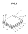
- a multilayer type piezoelectric filter according to an embodiment of the present invention is generally indicated by F and of the type having an S-P-S (series-parallel-series) structure.
- the piezoelectric filter F includes a series resonator S, a parallel resonator P and a series resonator S which are surrounded by respective frame-like spacers 2a, 2b and 2c and laminated one upon another with intermediate printed circuit boards 3a and 3b being interposed therebetween.
- a top printed circuit board 4 and a bottom printed circuit board 5 are disposed on the top of and under the bottom of the thus laminated resonators S, P and S.
- the frame-like spacers 2a, 2b and 2c and the printed circuit boards 4 and 5 are bonded together by means of adhesive sheets (not shown) and therefore hermetically sealed at the joining portions thereof.
- Each adhesive sheet is made of thermosetting resin and has a rectangular frame-like shape.
- the adhesive sheets are interposed between components, i.e., between the top printed circuit board 4 and the intermediate printed circuit board 3a, between the intermediate printed circuit boards 3a and 3b and between the intermediate printed circuit board 3b and the bottom printed circuit board 5 in a way as to extend along the peripheries thereof and bond or join them together by heating.
- the frame-like spacers 2a, 2b and 2c cooperate with the top printed circuit board 4, the intermediate printed circuit boards 3a and 3b and the bottom printed circuit board 5 to define therebetween chambers 6a, 6b and 6c for receiving therewithin the series resonator S, parallel resonator P and series resonator S, respectively.
- the resonators S, P and S are supported at the upper and lower surfaces thereof on the associated components, i.e., on the top printed circuit board 4 and the intermediate printed circuit board 3a, on the intermediate printed circuit boards 3a and 3b, and on the intermediate printed circuit board 3b and the bottom printed circuit board 5, respectively.
- each of the resonators S, S and P is made of lead titanate zirconate and has a square, thin plate-like shape.
- Each resonator consists of a piezoelectric ceramic substrate (no numeral) of a predetermined thickness and electrodes (not shown) formed on the upper and lower surfaces of the piezoelectric ceramic substrate.
- the parallel resonator P is thinner as compared with the series resonators S and S so as to have a large electrostatic capacity. By making smaller the thickness of the parallel resonator P as compared with that of the series resonators S, the difference in the capacity therebetween becomes large, thus making it possible to increase the attenuation or damping amount.
- each of the frame-like spacers 2a, 2b and 2c has at the front and rear edges thereof arcuate conductive grooves (no numeral) which are respectively aligned with conductive grooves (no numeral) at the edges of the intermediate printed circuit boards 3a and 3b, the top printed circuit board 4 and the bottom printed circuit board 5.
- a plurality of vertical conductive paths 12 are formed by the conductive grooves.
- the top printed circuit board 4 has at the lower surface thereof a conductive pattern including a circular land portion 14a.
- the conductive pattern is connected with one of the conductive grooves at the edge of the top printed circuit board 4.
- the conductive land portion 14a is connected to the central portion of the electrode on the upper surface of the series resonator S.
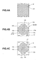
- each of the intermediate printed circuit boards 3a and 3b has at the upper surface thereof a conductive pattern 13a including four separate conductive surfaces 10a, 10b, 10b and 10b.
- a conductive pattern 13a including four separate conductive surfaces 10a, 10b, 10b and 10b.
- one conductive surface 10a is effective or actually operable and other three conductive surfaces 10b, 10b and 10b are dummy electrodes.
- a circular conductive land portion 14b which is connected by way of the effective conductive surface 10a to a conductive edge 15 constituting part of the arcuate conductive groove of the intermediate printed circuit boards 3a and 3b.
- each of the intermediate printed circuit boards 3a and 3b is formed a similar circular conductive land portion 14c (refer to Fig. 3).
- the conductive land portion 14b on the upper surface of the intermediate printed circuit board 3a is connected to the central portion of the electrode on the lower surface of the series resonator S (refer to Fig. 4A).
- the conductive land potion 14c on the lower surface of the intermediate printed circuit board 3a is connected to the central portion of the electrode on the upper surface of the parallel resonator P.
- the conductive land portion 14b on the upper surface of the intermediate printed circuit board 3b is connected to the central portion of the electrode on the lower surface of the parallel resonator P.
- the conductive land portion 14c on the lower surface of the intermediate printed circuit board 3b is connected to the central portion of the electrode on the upper surface of the series resonator S.
- the bottom printed circuit board 5 has on the upper surface thereof a conductive pattern 13b including four separate conductive surface portions 10a, 10b, 10b and 10b and a circular conductive land portion 14d.
- the conductive pattern 13b is connected to a conductive edge 17 constituting one of the arcuate conductive grooves of the bottom printed circuit board 5.
- an input electrode 18a and an output electrode 18b which are located adjacent the corners on the front edge side and a grounding electrode pad 18c which is located adjacent the center of the rear edge.
- the electrodes are connected to the respective conductive patterns 13a and 13b by way of the conductive paths 12.
- each printed circuit board can be uniform in the mechanical strength around the circular conductive land portion 14b or 14d.
- the multilayer type piezoelectric filter has an advantage of being capable of attaining an improved mechanical strength.
- the multilayer type piezoelectric filter F has such an S-P-S structure as described above.
- the piezoelectric filter F In case of mounting the piezoelectric filter F on a printed circuit board, i.e., in case the electrodes 18a, 18b and 18c on the lower surface of the piezoelectric filter F are connected by reflow soldering to corresponding portions of a printed circuit board, the piezoelectric filter F is exposed to heat of a high temperature. Further, the frame-like spacers 2a, 2b and 2c, the intermediate printed circuit boards 3a and 3b, the top printed circuit board 4 and the bottom printed circuit board 5 are joined together by heating of the adhesive sheets. To this end, the piezoelectric filter F is also placed within an atmosphere of a high temperature.
- the frame-like spacers 2a, 2b and 2c, the intermediate printed circuit boards 3a and 3b, the printed circuit board 4 and the bottom printed circuit board 5 are all made of glass epoxy and may be sized, by way of example, such that the intermediate printed circuit boards 3a and 3b are 0.1mm thick and the top printed circuit board 4 and the bottom printed circuit board 5 are 0.2mm thick.
- Such a multilayer type piezoelectric filter F is quite thin, i.e., the total thickness thereof is 1.8mm.
- the dimensions of the external shape is 6.5mm long and 5.5mm wide. The above described dimensions are shown for the purpose of illustration only and not for the purpose of limitation.
- the multilayer type piezoelectric filter F structured as described above is simple in structure, i.e., has a simple laminated structure and can be thin. Further, since the resonators S and P are protected by a casing consisting of the frame-like spacers 2a, 2b and 2c, the top printed circuit board 4 and the bottom printed circuit board 5, the piezoelectric filter F is strong and durable while enabling the resonators S and P to be protected mechanically and electrically. Furthermore, the piezoelectric filter F can be produced by simply laminating the plate-like components and the adhesive sheets and heating them. Thus, the piezoelectric filter F can be produced with ease and is therefore suited for mass production.
- a feature of the present invention resides in that the top printed circuit board 4 and the intermediate printed circuit boards 3a and 3b are formed with air vents or communication holes 20, 21a and 21b, respectively.
- the communication hole 20 provides communication between the chamber 6a and the outside or atmosphere.
- the communication hole 21a provides communication between the chambers 6a and 6b.
- the communication hole 21b provides communication between the chambers 6b and 6c.
- the pressure within the chambers 6a, 6b and 6c is prevented from becoming too high when the piezoelectric filter F is exposed to heat of a high temperature for electrically and mechanically connecting the electrode pads 18a, 18b and 18c to a printed circuit board by reflow soldering or when heated to a high temperature for bonding the frame-like spacers 2a, 2b and 2c, the intermediate printed circuit boards 3a and 3b, the top printed circuit board 4 and the bottom printed circuit board 5 together by means of the adhesive sheets.
- the communication hole 20 formed in the top printed circuit board 4 is formed so as to be smaller in diameter than the communication holes 21a and 21b.
- the communication hole 20 is 0.3mm in diameter and the communication holes 21a and 21b are 0.5mm in diameter.
- the diameter of the communication hole 20 is not limited to 0.3mm but can range from 0.1mm to 0.4mm.
- the diameter of the communication holes 21a and 21b is not limited to 0.5mm but can be 0.4mm or larger.
- the communication hole 21a formed in the upper, intermediate printed circuit board 3a can be smaller in diameter than the communication hole 21b formed in the lower, intermediate printed circuit board 3b so that higher one of the communication holes 20, 21a and 21b has a smaller diameter.
- the communication holes 20 and 21a are disposed at one and the other of opposite sides of the piezoelectric filter F so as to be distant or separate as much as possible.
- the communication holes 21b and 21a are respectively disposed at one and the other of the opposite sides so as to be distant or separate as much as possible.
- the communication holes 20, 21a and 21b are disposed alternately at one and the other of the opposite sides as shown in Fig. 3. More preferably, the communication holes 20 and 21a are respectively disposed at one and the other of diagonally opposite corners of the piezoelectric filter F so as to be distant or separate as much as possible.
- the communication holes 21b and 21a are respectively disposed at one and the other of the diagonally opposite corners so as to be distant or separate as much as possible. Namely, the communication holes 20, 21a and 21b are disposed alternately at one and the other of the diagonally opposite corners as shown in Fig. 2.
- the top printed circuit board 4 and the intermediate printed circuit boards 3a and 3b are respectively formed with the communication holes 20, 21a and 21b, thus allowing the chambers 6a, 6b and 6c to be communicated with the outside or the atmosphere. Accordingly, even when the piezoelectric filter F is heated up to a high temperature, substantial or excessive increase of the internal pressure is not caused and therefore it never occurs deformation of the outer casing, i.e., it never occurs that the top and bottom printed circuit boards 4 and 5 are curved or rounded outward. Further, with such a structure, the bottom printed circuit board 5 is not formed with any communication hole. By this, it never occurs that solder flows into the piezoelectric filter F through the communication hole.
- the filter F when the filter F is cooled down to a normal temperature after the air inside the piezoelectric filter F is discharged due to heat of a high temperature, the air containing moisture of the atmosphere may flow into the piezoelectric filter F, thus causing a possibility that the characteristics of the piezoelectric filter F are deteriorated and the conductive layers are shorted. Accordingly, it is desired that discharge of air inside the piezoelectric filter F due to heat of a high temperature is restricted so long as a variation of the internal pressure does not cause the top and bottom printed circuit board 4 and 5 to be curved or rounded outward.
- the communication hole 20 formed in the top printed circuit board 4 is smaller in diameter than the communication holes 21a and 21b formed in the intermediate printed circuit boards 3a and 3b, the air inside the chambers 6c and 6b is caused to flow out therefrom relatively with ease since the components of the piezoelectric filter F are heated to a high temperature in the order from a lower component to a higher component. A temperature rise of the chamber 6a located at an uppermost position is relatively smaller.
- the communication hole 20 which is formed in the top printed circuit board 4 so as to communicate directly with the atmosphere and have a relatively smaller diameter the air has a difficulty of flowing out due to the flow resistance so that the air inside the piezoelectric filter F generally has a difficulty of flowing out of the same.
- the communication holes 20, 21a and 21b are disposed alternately on the right-hand side and the lefthand side and spaced apart from each other along a side surface as much as possible.
- air flows from one side edge to the other side edge, i.e., flows zigzag.
- the heat of air is absorbed by the respective components of the piezoelectric filter F, thus causing a temperature fall of the air.
- the flow resistance is increased due to increase of the resistance of the surrounding or associated components and occurrence of a turbulent flow. By this increase of the flow resistance, the amount of air flowing out of the piezoelectric filter F is reduced. For this reason, when the piezoelectric filter F held within an atmosphere of a high temperature is moved therefrom and held within an atmosphere of a normal temperature, flow of the air into the chambers 6a, 6b and 6c is prevented or restricted.
- the internal pressure in the respective chambers 6a, 6b and 6c is adjusted optimally.
- an influence of heat due to reflow soldering or an influence of cooling on the piezoelectric filter F is prevented or restricted.
- the invention has been described above by reference to a certain embodiment of the invention, the invention is not limited to the embodiment described above. Modifications and variations of the embodiment described above will occur to those skilled in the art, in light of the above teachings.
- the multilayer type piezoelectric filter F of the S-P-S structure i.e., of the three-storied structure has been described and shown, it can be of the P-S-P structure or it can be of the two-storied structure or of the four-storied or more structure.
- the bottom printed circuit board 5 may be formed with a communication hole for providing communication between the chamber 6c and the outside.
- the communication hole is formed sufficiently small in diameter so as not to cause the solder to flow therethrough into the chamber 6c or the communication hole is formed at a place sufficiently separated or distant from the electrode pads 18a, 18b and 18c.
Landscapes
- Physics & Mathematics (AREA)
- Acoustics & Sound (AREA)
- Chemical & Material Sciences (AREA)
- Crystallography & Structural Chemistry (AREA)
- Piezo-Electric Or Mechanical Vibrators, Or Delay Or Filter Circuits (AREA)
Abstract
Description
Claims (12)
- A multilayer type piezoelectric filter (F) comprising:at least two laminated resonators (S, P or P, S);at least two frame-like spacers (2a, 2b or 2b, 2c) surrounding the resonators (S, P pr P, S), respectively;at least one intermediate printed circuit board (3a or 3b) interposed between the resonators (S, P or P, S) and between the frame-like spacers (2a, 2b or 2b, 2c);a top printed circuit board (4) disposed on the resonators (S, P) and the frame-like spacers (2a, 2b or 2b, 2c) to cooperate with one of the frame-like spacers (2a, 2b or 2b, 2c) and the intermediate printed circuit board (3a or 3b) to define therebetween a first chamber (6a or 6b) within which one of the resonators (S, P or P, S) is disposed;a bottom printed circuit board (5) disposed under the resonators (S, P or P, S)) and the frame-like spacers (2a, 2b or 2b, 2c) to cooperate with the other of the frame-like spacers (2a, 2b or 2b, 2c) and the intermediate printed circuit board (3a or 3b) to define therebetween a second chamber (6b or 6c) within which the other of the resonators (S, P or P, S) is disposed;a plurality of electrode pads (18a, 18b, 18c) formed on a lower surface of the bottom printed circuit board (5);a first communication hole (21a or 21b) formed in the intermediate printed circuit board (3a or 3b) for providing communication between the first chamber (6a or 6b) and the second chamber (6b or 6c); anda second communication hole (20) formed in the top printed circuit board (4) for providing communication between the first chamber (6a or 6b) and the outside.
- A multilayer type piezoelectric filter (F) according to claim 1, wherein the second communication hole (20) is smaller in diameter than the first communication hole (21a or 21b).
- A multilayer type piezoelectric filter (F) according to claim 1, being generally rectangular when observed in plan, wherein the first communication hole (21a or 21b) is disposed adjacent one of opposite sides of the piezoelectric filter (F) and the second communication hole (20) is disposed adjacent the other of the opposite sides when observed in plan.
- A multilayer type piezoelectric filter (F) according to claim 1, being generally rectangular when observed in plan, and wherein the first communication hole (21a or 21b) is disposed adjacent one of diagonally opposite corners of the piezoelectric filter (F) and the second communication hole (20) is disposed adjacent the other of the diagonally opposite corners when observed in plan.
- A multilayer type piezoelectric filter (F) according to claim 1, wherein the frame-like spacers (2a, 2b or 2b, 2c), the top printed circuit board (4) and the bottom printed circuit board (5) are bonded together and hermetically sealed at joining portions thereof.
- A multilayer type piezoelectric filter (F) comprising:a plurality of resonators (S, P, S) laminated one upon the other;a plurality of frame-like spacers (2a, 2b, 2c) surrounding the resonators (S, P, S), respectively;a plurality of intermediate printed circuit boards (3a, 3b) interposed between adjacent two of the resonators (S, P, S) and between adjacent two of the frame-like spacers (2a, 2b, 2c);a top printed circuit board (4) disposed on the resonators (S, P, S) and the frame-like spacers (2a, 2b, 2c) to cooperate with associated one of the frame-like spacers (2a, 2b, 2c) and associated one of the intermediate printed circuit boards (3a, 3b) to define therebetween a first chamber (6a);the intermediate printed circuit boards (3a, 3b) cooperating with the frame-like spacers (3a, 3b) to define therebetween at least one second chamber (6b);a bottom printed circuit board (5) disposed under the resonators (S, P, S) and the frame-like spacers (2a, 2b, 2c) to cooperate with associated one of the frame-like spacers (2a, 2b, 2c) and associated one of the intermediate printed circuit boards (3a, 3b) to define therebetween a third chamber (6c);the resonators (S, P, S) being disposed within the first chamber (6a), the second chamber (6b) and the third chamber (6c), respectively;the frame-like spacers (2a, 2b, 2c), the top printed circuit board (4) and the bottom printed circuit board (5) being bonded together and hermetically sealed at joining portions thereof;a plurality of electrode pads (18a, 18b, 18c) formed on a lower surface of the bottom printed circuit board (5);a plurality of first vents (21a, 21b) formed in the intermediate printed circuit boards (3a, 3b) for providing communication between the first chamber (6a) and the second chamber (6b) and between the second chamber (6b) and the third chamber (6c); anda second vent (20) formed in the top printed circuit board (4) for providing communication between the first chamber (6a) and the outside.
- A multilayer type piezoelectric filter (F) according to claim 6, wherein one (21a) of the first vents formed in upper one (3a) of the intermediate printed circuit boards is smaller in diameter than another (21b) of the first vents formed in lower one (3b) of the intermediate printed circuit boards.
- A multilayer type piezoelectric filter (F) according to claim 7, wherein the second vent (20) is smaller in diameter than one (21a) of the first vents formed in upper one (3a) of the intermediate printed circuit boards.
- A multilayer type piezoelectric filter (F) according to claim 6, being generally rectangular when observed in plan, wherein one (21a) of the first vents formed in the upper one (3a) of the intermediate printed circuit boards is located adjacent one of diagonally opposite corners of the piezoelectric filter (F), and another (21b) of the first vents formed in lower one (3b) of the intermediate printed circuit boards and the second vent (20) are located adjacent the other of the diagonally opposite corners when observed in plan.
- A multilayer type piezoelectric filter (F) according to claim 6, wherein the number of the resonators (S, P, S) is three, one (P) of the resonators is a parallel resonator and the other two (S) are series resonators to constitute a filter circuit of an S-P-S structure.
- A multilayer type piezoelectric filter (F) according to claim 6, wherein the number of the resonators (P, S, P)) is three, one (S) of the resonators is a series resonator and the other two (P) are parallel resonators to constitute a filter circuit of an P-S-P structure.
- A multilayer type piezoelectric filter (F) according to claim 6, wherein the first vents (21a, 21b) are 0.4mn or larger in diameter, and the second vent (20) ranges in diameter from 0.1 to 0.4mm.
Applications Claiming Priority (2)
| Application Number | Priority Date | Filing Date | Title |
|---|---|---|---|
| JP2000264101 | 2000-08-31 | ||
| JP2000264101A JP2002076837A (en) | 2000-08-31 | 2000-08-31 | Multilayer piezoelectric filter |
Publications (2)
| Publication Number | Publication Date |
|---|---|
| EP1187325A2 true EP1187325A2 (en) | 2002-03-13 |
| EP1187325A3 EP1187325A3 (en) | 2008-08-06 |
Family
ID=18751563
Family Applications (1)
| Application Number | Title | Priority Date | Filing Date |
|---|---|---|---|
| EP01120910A Withdrawn EP1187325A3 (en) | 2000-08-31 | 2001-08-30 | Multilayer type piezoelectric filter |
Country Status (3)
| Country | Link |
|---|---|
| US (1) | US6590474B2 (en) |
| EP (1) | EP1187325A3 (en) |
| JP (1) | JP2002076837A (en) |
Families Citing this family (3)
| Publication number | Priority date | Publication date | Assignee | Title |
|---|---|---|---|---|
| US8618720B2 (en) * | 2009-10-01 | 2013-12-31 | Blackberry Limited | Piezoelectric assembly |
| JP6835971B2 (en) * | 2017-08-04 | 2021-02-24 | 株式会社フジクラ | Manufacturing method of multi-layer printed wiring board and multi-layer printed wiring board |
| US10638608B2 (en) | 2017-09-08 | 2020-04-28 | Apple Inc. | Interconnect frames for SIP modules |
Family Cites Families (8)
| Publication number | Priority date | Publication date | Assignee | Title |
|---|---|---|---|---|
| JPH044603A (en) * | 1990-04-21 | 1992-01-09 | Murata Mfg Co Ltd | Chip type piezoelectric component |
| JPH06224687A (en) * | 1993-01-28 | 1994-08-12 | Murata Mfg Co Ltd | Ladder type filter |
| JPH0918285A (en) * | 1995-06-30 | 1997-01-17 | Kyocera Corp | Ladder type filter |
| US6114800A (en) * | 1997-10-01 | 2000-09-05 | Murata Manufacturing Co., Ltd | Piezoelectric component |
| JP2000077971A (en) * | 1998-08-28 | 2000-03-14 | Ngk Spark Plug Co Ltd | Multilayer piezoelectric filter |
| JP3610477B2 (en) | 1998-12-17 | 2005-01-12 | 日本特殊陶業株式会社 | Multilayer piezoelectric filter |
| JP2000223983A (en) | 1999-02-03 | 2000-08-11 | Ngk Spark Plug Co Ltd | Conduction method of multilayer piezoelectric filter |
| JP2000223982A (en) | 1999-02-03 | 2000-08-11 | Ngk Spark Plug Co Ltd | Conduction method of multilayer piezoelectric filter |
-
2000
- 2000-08-31 JP JP2000264101A patent/JP2002076837A/en active Pending
-
2001
- 2001-08-30 US US09/941,739 patent/US6590474B2/en not_active Expired - Fee Related
- 2001-08-30 EP EP01120910A patent/EP1187325A3/en not_active Withdrawn
Also Published As
| Publication number | Publication date |
|---|---|
| EP1187325A3 (en) | 2008-08-06 |
| US20020024408A1 (en) | 2002-02-28 |
| US6590474B2 (en) | 2003-07-08 |
| JP2002076837A (en) | 2002-03-15 |
Similar Documents
| Publication | Publication Date | Title |
|---|---|---|
| JP2002330044A (en) | Surface mount electronic components | |
| JP3218971B2 (en) | Ladder type filter | |
| US5825262A (en) | Ladder filter with piezoelectric resonators each having a plurality of layers with internal electrodes | |
| JP3427032B2 (en) | Electret condenser microphone | |
| US6246013B1 (en) | Surface mounting structure and surface mount type electronic component included therein | |
| US5925971A (en) | Piezoelectric resonator and electronic component containing same | |
| US6590474B2 (en) | Multilayer piezoelectric filter with an air vent between two resonator chambers | |
| US5394123A (en) | Ladder type filter comprised of stacked tuning fork type resonators | |
| JPH09270669A (en) | Ladder filter | |
| JPH04284015A (en) | Ladder-type filter | |
| US6420945B1 (en) | Piezoelectric resonator having internal electrode films, piezoelectric component and ladder filter formed therefrom | |
| JP3413657B2 (en) | Manufacturing method of package for surface mount type piezoelectric vibrator | |
| JPS6359012A (en) | Composite electronic component | |
| KR100490501B1 (en) | Piezoelectric vibrator and fabricating method therefor | |
| US6225877B1 (en) | Multilayer type piezoelectric filter with intermediary printed circuit board elements | |
| JP3610477B2 (en) | Multilayer piezoelectric filter | |
| EP0821482A2 (en) | Piezoelectric resonator and electric component using the same | |
| JP2003086755A (en) | Hybrid module | |
| JPS62122312A (en) | Piezoelectric resonator built-in capacitor | |
| JP2003023336A (en) | Mounting electronic components such as multilayer piezoelectric filters | |
| JP2002314369A (en) | Multilayer piezoelectric filter | |
| JP2536627B2 (en) | Chip-shaped piezoelectric component | |
| JP3993399B2 (en) | Chip-type piezoelectric filter | |
| JP2006100680A (en) | Electronic device package, manufacturing method thereof, and piezoelectric device | |
| JP2000031774A (en) | Piezo filter |
Legal Events
| Date | Code | Title | Description |
|---|---|---|---|
| PUAI | Public reference made under article 153(3) epc to a published international application that has entered the european phase |
Free format text: ORIGINAL CODE: 0009012 |
|
| AK | Designated contracting states |
Kind code of ref document: A2 Designated state(s): AT BE CH CY DE DK ES FI FR GB GR IE IT LI LU MC NL PT SE TR |
|
| AX | Request for extension of the european patent |
Free format text: AL;LT;LV;MK;RO;SI |
|
| PUAL | Search report despatched |
Free format text: ORIGINAL CODE: 0009013 |
|
| AK | Designated contracting states |
Kind code of ref document: A3 Designated state(s): AT BE CH CY DE DK ES FI FR GB GR IE IT LI LU MC NL PT SE TR |
|
| AX | Request for extension of the european patent |
Extension state: AL LT LV MK RO SI |
|
| AKX | Designation fees paid | ||
| STAA | Information on the status of an ep patent application or granted ep patent |
Free format text: STATUS: THE APPLICATION IS DEEMED TO BE WITHDRAWN |
|
| 18D | Application deemed to be withdrawn |
Effective date: 20090207 |
|
| REG | Reference to a national code |
Ref country code: DE Ref legal event code: 8566 |