EP1187202A2 - Semiconductor package - Google Patents
Semiconductor package Download PDFInfo
- Publication number
- EP1187202A2 EP1187202A2 EP01121166A EP01121166A EP1187202A2 EP 1187202 A2 EP1187202 A2 EP 1187202A2 EP 01121166 A EP01121166 A EP 01121166A EP 01121166 A EP01121166 A EP 01121166A EP 1187202 A2 EP1187202 A2 EP 1187202A2
- Authority
- EP
- European Patent Office
- Prior art keywords
- die
- pad
- semiconductor device
- wires
- silver
- Prior art date
- Legal status (The legal status is an assumption and is not a legal conclusion. Google has not performed a legal analysis and makes no representation as to the accuracy of the status listed.)
- Ceased
Links
Images



Classifications
-
- H—ELECTRICITY
- H10—SEMICONDUCTOR DEVICES; ELECTRIC SOLID-STATE DEVICES NOT OTHERWISE PROVIDED FOR
- H10W—GENERIC PACKAGES, INTERCONNECTIONS, CONNECTORS OR OTHER CONSTRUCTIONAL DETAILS OF DEVICES COVERED BY CLASS H10
- H10W74/00—Encapsulations, e.g. protective coatings
- H10W74/01—Manufacture or treatment
- H10W74/019—Manufacture or treatment using temporary auxiliary substrates
-
- H—ELECTRICITY
- H10—SEMICONDUCTOR DEVICES; ELECTRIC SOLID-STATE DEVICES NOT OTHERWISE PROVIDED FOR
- H10P—GENERIC PROCESSES OR APPARATUS FOR THE MANUFACTURE OR TREATMENT OF DEVICES COVERED BY CLASS H10
- H10P72/00—Handling or holding of wafers, substrates or devices during manufacture or treatment thereof
- H10P72/70—Handling or holding of wafers, substrates or devices during manufacture or treatment thereof for supporting or gripping
- H10P72/74—Handling or holding of wafers, substrates or devices during manufacture or treatment thereof for supporting or gripping using temporarily an auxiliary support
-
- H—ELECTRICITY
- H10—SEMICONDUCTOR DEVICES; ELECTRIC SOLID-STATE DEVICES NOT OTHERWISE PROVIDED FOR
- H10W—GENERIC PACKAGES, INTERCONNECTIONS, CONNECTORS OR OTHER CONSTRUCTIONAL DETAILS OF DEVICES COVERED BY CLASS H10
- H10W70/00—Package substrates; Interposers; Redistribution layers [RDL]
- H10W70/40—Leadframes
- H10W70/411—Chip-supporting parts, e.g. die pads
-
- H—ELECTRICITY
- H10—SEMICONDUCTOR DEVICES; ELECTRIC SOLID-STATE DEVICES NOT OTHERWISE PROVIDED FOR
- H10W—GENERIC PACKAGES, INTERCONNECTIONS, CONNECTORS OR OTHER CONSTRUCTIONAL DETAILS OF DEVICES COVERED BY CLASS H10
- H10W70/00—Package substrates; Interposers; Redistribution layers [RDL]
- H10W70/40—Leadframes
- H10W70/456—Materials
- H10W70/457—Materials of metallic layers on leadframes
-
- H—ELECTRICITY
- H10—SEMICONDUCTOR DEVICES; ELECTRIC SOLID-STATE DEVICES NOT OTHERWISE PROVIDED FOR
- H10W—GENERIC PACKAGES, INTERCONNECTIONS, CONNECTORS OR OTHER CONSTRUCTIONAL DETAILS OF DEVICES COVERED BY CLASS H10
- H10W74/00—Encapsulations, e.g. protective coatings
- H10W74/01—Manufacture or treatment
- H10W74/014—Manufacture or treatment using batch processing
-
- H—ELECTRICITY
- H10—SEMICONDUCTOR DEVICES; ELECTRIC SOLID-STATE DEVICES NOT OTHERWISE PROVIDED FOR
- H10W—GENERIC PACKAGES, INTERCONNECTIONS, CONNECTORS OR OTHER CONSTRUCTIONAL DETAILS OF DEVICES COVERED BY CLASS H10
- H10W74/00—Encapsulations, e.g. protective coatings
- H10W74/10—Encapsulations, e.g. protective coatings characterised by their shape or disposition
- H10W74/111—Encapsulations, e.g. protective coatings characterised by their shape or disposition the semiconductor body being completely enclosed
-
- H—ELECTRICITY
- H10—SEMICONDUCTOR DEVICES; ELECTRIC SOLID-STATE DEVICES NOT OTHERWISE PROVIDED FOR
- H10W—GENERIC PACKAGES, INTERCONNECTIONS, CONNECTORS OR OTHER CONSTRUCTIONAL DETAILS OF DEVICES COVERED BY CLASS H10
- H10W72/00—Interconnections or connectors in packages
- H10W72/01—Manufacture or treatment
- H10W72/0198—Manufacture or treatment batch processes
-
- H—ELECTRICITY
- H10—SEMICONDUCTOR DEVICES; ELECTRIC SOLID-STATE DEVICES NOT OTHERWISE PROVIDED FOR
- H10W—GENERIC PACKAGES, INTERCONNECTIONS, CONNECTORS OR OTHER CONSTRUCTIONAL DETAILS OF DEVICES COVERED BY CLASS H10
- H10W72/00—Interconnections or connectors in packages
- H10W72/071—Connecting or disconnecting
- H10W72/075—Connecting or disconnecting of bond wires
-
- H—ELECTRICITY
- H10—SEMICONDUCTOR DEVICES; ELECTRIC SOLID-STATE DEVICES NOT OTHERWISE PROVIDED FOR
- H10W—GENERIC PACKAGES, INTERCONNECTIONS, CONNECTORS OR OTHER CONSTRUCTIONAL DETAILS OF DEVICES COVERED BY CLASS H10
- H10W72/00—Interconnections or connectors in packages
- H10W72/071—Connecting or disconnecting
- H10W72/075—Connecting or disconnecting of bond wires
- H10W72/07551—Connecting or disconnecting of bond wires characterised by changes in properties of the bond wires during the connecting
- H10W72/07554—Connecting or disconnecting of bond wires characterised by changes in properties of the bond wires during the connecting changes in dispositions
-
- H—ELECTRICITY
- H10—SEMICONDUCTOR DEVICES; ELECTRIC SOLID-STATE DEVICES NOT OTHERWISE PROVIDED FOR
- H10W—GENERIC PACKAGES, INTERCONNECTIONS, CONNECTORS OR OTHER CONSTRUCTIONAL DETAILS OF DEVICES COVERED BY CLASS H10
- H10W72/00—Interconnections or connectors in packages
- H10W72/50—Bond wires
-
- H—ELECTRICITY
- H10—SEMICONDUCTOR DEVICES; ELECTRIC SOLID-STATE DEVICES NOT OTHERWISE PROVIDED FOR
- H10W—GENERIC PACKAGES, INTERCONNECTIONS, CONNECTORS OR OTHER CONSTRUCTIONAL DETAILS OF DEVICES COVERED BY CLASS H10
- H10W72/00—Interconnections or connectors in packages
- H10W72/50—Bond wires
- H10W72/541—Dispositions of bond wires
- H10W72/5449—Dispositions of bond wires not being orthogonal to a side surface of the chip, e.g. fan-out arrangements
-
- H—ELECTRICITY
- H10—SEMICONDUCTOR DEVICES; ELECTRIC SOLID-STATE DEVICES NOT OTHERWISE PROVIDED FOR
- H10W—GENERIC PACKAGES, INTERCONNECTIONS, CONNECTORS OR OTHER CONSTRUCTIONAL DETAILS OF DEVICES COVERED BY CLASS H10
- H10W72/00—Interconnections or connectors in packages
- H10W72/50—Bond wires
- H10W72/541—Dispositions of bond wires
- H10W72/547—Dispositions of multiple bond wires
-
- H—ELECTRICITY
- H10—SEMICONDUCTOR DEVICES; ELECTRIC SOLID-STATE DEVICES NOT OTHERWISE PROVIDED FOR
- H10W—GENERIC PACKAGES, INTERCONNECTIONS, CONNECTORS OR OTHER CONSTRUCTIONAL DETAILS OF DEVICES COVERED BY CLASS H10
- H10W72/00—Interconnections or connectors in packages
- H10W72/50—Bond wires
- H10W72/551—Materials of bond wires
- H10W72/552—Materials of bond wires comprising metals or metalloids, e.g. silver
- H10W72/5525—Materials of bond wires comprising metals or metalloids, e.g. silver comprising copper [Cu]
-
- H—ELECTRICITY
- H10—SEMICONDUCTOR DEVICES; ELECTRIC SOLID-STATE DEVICES NOT OTHERWISE PROVIDED FOR
- H10W—GENERIC PACKAGES, INTERCONNECTIONS, CONNECTORS OR OTHER CONSTRUCTIONAL DETAILS OF DEVICES COVERED BY CLASS H10
- H10W72/00—Interconnections or connectors in packages
- H10W72/50—Bond wires
- H10W72/59—Bond pads specially adapted therefor
-
- H—ELECTRICITY
- H10—SEMICONDUCTOR DEVICES; ELECTRIC SOLID-STATE DEVICES NOT OTHERWISE PROVIDED FOR
- H10W—GENERIC PACKAGES, INTERCONNECTIONS, CONNECTORS OR OTHER CONSTRUCTIONAL DETAILS OF DEVICES COVERED BY CLASS H10
- H10W72/00—Interconnections or connectors in packages
- H10W72/90—Bond pads, in general
- H10W72/931—Shapes of bond pads
- H10W72/932—Plan-view shape, i.e. in top view
-
- H—ELECTRICITY
- H10—SEMICONDUCTOR DEVICES; ELECTRIC SOLID-STATE DEVICES NOT OTHERWISE PROVIDED FOR
- H10W—GENERIC PACKAGES, INTERCONNECTIONS, CONNECTORS OR OTHER CONSTRUCTIONAL DETAILS OF DEVICES COVERED BY CLASS H10
- H10W72/00—Interconnections or connectors in packages
- H10W72/90—Bond pads, in general
- H10W72/951—Materials of bond pads
-
- H—ELECTRICITY
- H10—SEMICONDUCTOR DEVICES; ELECTRIC SOLID-STATE DEVICES NOT OTHERWISE PROVIDED FOR
- H10W—GENERIC PACKAGES, INTERCONNECTIONS, CONNECTORS OR OTHER CONSTRUCTIONAL DETAILS OF DEVICES COVERED BY CLASS H10
- H10W72/00—Interconnections or connectors in packages
- H10W72/90—Bond pads, in general
- H10W72/951—Materials of bond pads
- H10W72/952—Materials of bond pads comprising metals or metalloids, e.g. PbSn, Ag or Cu
-
- H—ELECTRICITY
- H10—SEMICONDUCTOR DEVICES; ELECTRIC SOLID-STATE DEVICES NOT OTHERWISE PROVIDED FOR
- H10W—GENERIC PACKAGES, INTERCONNECTIONS, CONNECTORS OR OTHER CONSTRUCTIONAL DETAILS OF DEVICES COVERED BY CLASS H10
- H10W74/00—Encapsulations, e.g. protective coatings
-
- H—ELECTRICITY
- H10—SEMICONDUCTOR DEVICES; ELECTRIC SOLID-STATE DEVICES NOT OTHERWISE PROVIDED FOR
- H10W—GENERIC PACKAGES, INTERCONNECTIONS, CONNECTORS OR OTHER CONSTRUCTIONAL DETAILS OF DEVICES COVERED BY CLASS H10
- H10W74/00—Encapsulations, e.g. protective coatings
- H10W74/10—Encapsulations, e.g. protective coatings characterised by their shape or disposition
- H10W74/111—Encapsulations, e.g. protective coatings characterised by their shape or disposition the semiconductor body being completely enclosed
- H10W74/127—Encapsulations, e.g. protective coatings characterised by their shape or disposition the semiconductor body being completely enclosed characterised by arrangements for sealing or adhesion
-
- H—ELECTRICITY
- H10—SEMICONDUCTOR DEVICES; ELECTRIC SOLID-STATE DEVICES NOT OTHERWISE PROVIDED FOR
- H10W—GENERIC PACKAGES, INTERCONNECTIONS, CONNECTORS OR OTHER CONSTRUCTIONAL DETAILS OF DEVICES COVERED BY CLASS H10
- H10W90/00—Package configurations
- H10W90/701—Package configurations characterised by the relative positions of pads or connectors relative to package parts
- H10W90/751—Package configurations characterised by the relative positions of pads or connectors relative to package parts of bond wires
- H10W90/756—Package configurations characterised by the relative positions of pads or connectors relative to package parts of bond wires between a chip and a stacked lead frame, conducting package substrate or heat sink
Definitions
- the present invention relates to a semiconductor package in which a semiconductor device is mounted on a lead frame and the outside thereof, particularly the upper surface of semiconductor device is encapsulated with molding compound.
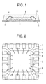
- Fig. 1 is a sectional view of one example of semiconductor package.
- Fig. 2 is a plan view thereof seen through molding compound.
- the semiconductor package shown in Figs. 1 and 2 is comprised of a lead frame 1, a semiconductor device 4 mounted on die-pad 3 supported with suspending leads 2 of lead frame 1, metallic thin wires 6 electrically connecting electrodes provided on the top face of the semiconductor device 4 with terminals 5 of lead frame 1, respectively and molding compound 7 for encapsulating the outside region of semiconductor device 4 including the upper side of semiconductor device 4 and the lower side of die-pad 3.
- the semiconductor package is of so-called non-lead type in which outer leads are not projected from the semiconductor package and the two of inner leads and outer leads are integrated into terminals 5, wherein in used lead flame 1, suspending leads 2 are directed upward in such a manner that die-pad 3 is positioned higher than terminals 5. Since such a step is provided between die pads 3 and terminals 5, molding compound 7 can be inserted into the lower side of die-pad 3.
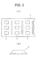
- a matrix type frame is mainly used for the above-mentioned non-lead type of semiconductor package, in which plural semiconductor devices are arranged in a direction of a width of the matrix type frame. Further, recently, from a demand for cost down, it is thought to switch over a frame of individually molding type shown in Fig. 3 to a frame of collectively molding type shown in Fig.4.
- Fig. 3(A) In the frame of individually molding type, as shown in Fig. 3(A), individual molding cavities C of small size are provided separately within a frame F. After molding, individual semiconductor packages are stamped out so that semiconductor packages S shown in Fig. 3(B) are obtained. Namely, semiconductor devices are mounted on die-pads of lead frames through silver paste and others, and wire bonding is carried out. Thereafter, respective semiconductor devices are individually molded with molding compound and the molded semiconductor devices are stamped out to form individual semiconductor packages.
- Fig. 4(A) In the frame of collectively molding type, as shown in Fig. 4(A), some molding cavities C of large size are provided within a frame F. Multiple semiconductor devices are arranged in matrix within each molding cavity C, respectively and collectively molded with molding compound. Thereafter, the collectively molded semiconductor devices are cut at grid-leads L by means of dicing saw so that a semiconductor package S shown in Fig. 4(B) is obtained. Namely, semiconductor devices are mounted on die-pads of lead frames through silver pastes and others and wire bonding is carried out. Thereafter, plural semiconductor devices arranged are collectively molded with molding compound to a given cavity size, and then the collectively molded semiconductor devices are cut to form individual semiconductor packages by dicing.
- a type of semiconductor package in which a die-pad is exposed to increase the effect of heat radiation and bonding of some electrodes of semiconductor device to the surface of die-pad 3 for grounding is needed.
- Fig. 5 is a sectional view of such a type of semiconductor package.
- Fig. 6 is a plan view of the semiconductor package seen through molding compound thereof.
- semiconductor devices are correctively molded with molding compound 7, and then as above-mentioned, the collectively molded semiconductor devices are cut to form individual semiconductor packages.
- silver plating (not shown) is made on the wire connecting points of terminals 5 in lead frame 1, while in a type of semiconductor package shown in Fig. 5, silver plating is made also on the surface of die-pad 3.
- solder plating is made not only on the exposed portions of terminals 5, but also on the exposed portions of die-pad 3. Further, solder cream is applied on areas on printed circuit board corresponding to the exposed portions of terminals 5 and die-pad 3.
- Semiconductor package mounted on a printed circuit board is heated in an oven at about 230°C, by which solder is made re-flow so that semiconductor package is fixed firmly at a given position on a printed circuit board.
- a semiconductor package of the present invention comprises a semiconductor device mounted on a die-pad supported by suspending leads of a lead frame, wires for electrically connecting given electrodes arranged on a top face of the semiconductor device with terminals of the lead frame, wires for bonding the other electrodes arranged on the top face of the semiconductor device to the surface of the die-pad for grounding and molding compound for encapsulating an outer area of the semiconductor device including all the wires, while the lower face of die-pad and the lower face and side face of terminals are exposed, wherein portion(s) plated with silver for connecting of wires on the surface of the die-pad are formed at points positioned between a peripheral edge of the die-pad and an outer edge of the semiconductor device with leaving spaces from both the edges.
- Fig. 7 is a sectional view of one example of semiconductor package according to the present invention.
- Fig. 8 is a plan view showing a state of the semiconductor package seen through molding compound.
- the semiconductor package is a collectively molding type of semiconductor package as shown in Figs. 7 and 8.
- the semiconductor package comprises a semiconductor device 4 mounted on a die-pad 3 supported by suspending leads 2 of a lead frame 1, wires 6 for electrically connecting given electrodes 9 arranged on a top face of the semiconductor device 4 with terminals 5 of the lead frame, wires 8 for bonding the other electrodes 10 arranged on the top face of semiconductor device 4 to the surface of the die-pad for grounding and molding compound 7 for encapsulating an outer area of semiconductor device 4 including all the wires 6, 8, while the lower face of die-pad 3 and the lower face and side face of terminals 5 are exposed.
- portions 11 plated with silver are formed in wire-connection parts of terminals 5, and portion 12 plated with silver for connecting of wires is formed on the surface of die-pad 3. Portions 11, 12 plated with silver are shown with hatching in Fig. 8 in order to make easy to read the figure.
- Portion 12 plated with silver on the surface of die-pad 3 is, as shown in Fig. 8, formed into a shape of line between a peripheral edge of die-pad 3 and an outer edge of semiconductor device 4 with leaving spaces from both the edges. Accordingly, molding compound 7 is made into contact not only with portion 12 plated with silver but also with copper material of lead frame on both sides of the linear shaped area plated with silver. Therefore, adhesion of portion plated with silver to molding compound 7 is improved as compared with a case where all molding compound 7 is made into contact with portion plated with silver.
- portion 12 plated with silver is formed continuously.
- portion 12 plated with silver may be divided into a plurality of portions plated with silver formed into a form of islands only to parts of die-pad 3 to be connected with wire 8.
- the discontinuous forming of portions 12 plated with silver in such a manner makes an area of resin 7 made into contact with copper surface of lead frame larger so that the adhesion of resin 7 to portions 12 plated with silver is improved.
- portions 11, 12 plated with silver are formed on a frame in which a plurality of lead frames 1 are arranged in matrix, in the same manner as conventional case, wherein however, portions 12 plated with silver on die-pad 3 are formed into a linear shape or discontinuously, differently from conventional case.
- Fig. 9 is a sectional view of another example of semiconductor package according to the present invention.
- Fig. 10 is a plan view of the semiconductor package, showing a state thereof seen through molding compound.
- the semiconductor package is nearly the same as the example shown in Figs. 7 and 8, wherein however, this semiconductor package has concave portions 13, 14 formed along both sides of portion 12 plated with silver for connecting of wires on the surface of die-pad 3. Since molding compound 7 is inserted into the concave portions 13, 14 in this semiconductor package, the adhesion of molding compound 7 to die-pad 3 is further improved.
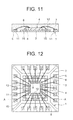
- Fig. 11 is a sectional view of further example of semiconductor package according to the present invention.
- Fig. 12 is a plan view showing a state of the semiconductor package seen through molding compound.
- Fig. 13 is a sectional view taken on line A-A of Fig. 12.
- the semiconductor package shown in Fig. 11 differs from the first example shown in Figs. 7 and 8 in the structure of the portion 12 plated with silver for connection of wires on the surface of die-pad 3. That is, portions plated with silver for connection of wires are formed discontinuously. And concave portions 15 are formed between discontinuous portions 12 plated with silver. In the semiconductor package, since molding compound 7 penetrates into these concave portions 15, the adhesion of molding compound 7 to die-pad 3 is further increased.
- through hole(s) can be applied instead of concave portions 15, by which the adhesion of molding compound 7 to die-pad 3 can be increased.
- the above-mentioned concave portions can be formed by half-cutting by etching or impressing of material of lead frame, when forming a lead frame. Further, through holes can be formed by etching material of lead frame from both sides of the material or stamping the material.
- the semiconductor package of the present invention comprises a semiconductor device mounted on a die-pad supported by suspending leads of a lead frame, wires for electrically connecting given electrodes arranged on a top face of the semiconductor device with terminals of the semiconductor device, wires for bonding the other electrodes arranged on the top face of the semiconductor device to the surface of the die-pad for grounding and molding compound with which an outer area of the semiconductor device including all the wires is encapsulated, wherein portions plated with silver for connecting of wires on the surface of the die-pad are formed at points positioned between a peripheral edge of the die-pad and an outer edge of the semiconductor device with leaving spaces from both the edges.
- molding compound is also made into contact with copper material of lead frame so that the adhesion of die-pad to molding compound is increased. Therefore, the reliability can be secured that no trouble of coming-off of wires or cutting of wires occur in mounting a semiconductor package on a printed circuit board.
Landscapes
- Structures Or Materials For Encapsulating Or Coating Semiconductor Devices Or Solid State Devices (AREA)
- Lead Frames For Integrated Circuits (AREA)
Abstract
Description
Claims (7)
- A semiconductor package comprising a semiconductor device mounted on a die-pad supported by suspending leads of a lead frame, wires for electrically connecting given electrodes arranged on a top face of the semiconductor device with terminals of the lead frame, wires for bonding the other electrodes arranged on the top face of the semiconductor device to the surface of the die-pad for grounding and molding compound with which an outer area of the semiconductor device including all the wires is encapsulated, wherein portion(s) plated with silver for connecting of wires on the surface of the die-pad are formed at points positioned between a peripheral edge of the die-pad and an outer edge of the semiconductor device with leaving spaces from both the edges.
- A semiconductor package as claimed in claim 1, wherein the portion plated with silver for connecting of wires on the surface of the die-pads is formed into a shape of line.
- A semiconductor device as claimed in claim 1, wherein the portion plated with silver for connecting of wires on the surface of the die-pad is formed into a shape of line and at least a concave portion is formed along one side of the linear shaped area plated with silver.
- A semiconductor device as claimed in claim 1, wherein the concave portion is provided with through hole(s) formed leaving at least a part of the concave portion.
- A semiconductor device as claimed in claim 1, wherein the portions plated with silver for connecting of wires on the surface of the die-pad are formed discontinuously.
- A semiconductor device as claimed in claim 5, wherein concave portions are formed between the discontinuous portions plated with silver.
- A semiconductor device as claimed in claim 1, wherein through holes are formed between the discontinuous portions plated with silver.
Priority Applications (1)
| Application Number | Priority Date | Filing Date | Title |
|---|---|---|---|
| EP06004143A EP1662565B1 (en) | 2000-09-04 | 2001-09-04 | Semiconductor package |
Applications Claiming Priority (2)
| Application Number | Priority Date | Filing Date | Title |
|---|---|---|---|
| JP2000266704A JP2002076228A (en) | 2000-09-04 | 2000-09-04 | Resin-sealed semiconductor device |
| JP2000266704 | 2000-09-04 |
Related Child Applications (1)
| Application Number | Title | Priority Date | Filing Date |
|---|---|---|---|
| EP06004143A Division EP1662565B1 (en) | 2000-09-04 | 2001-09-04 | Semiconductor package |
Publications (2)
| Publication Number | Publication Date |
|---|---|
| EP1187202A2 true EP1187202A2 (en) | 2002-03-13 |
| EP1187202A3 EP1187202A3 (en) | 2004-08-25 |
Family
ID=18753746
Family Applications (2)
| Application Number | Title | Priority Date | Filing Date |
|---|---|---|---|
| EP06004143A Expired - Lifetime EP1662565B1 (en) | 2000-09-04 | 2001-09-04 | Semiconductor package |
| EP01121166A Ceased EP1187202A3 (en) | 2000-09-04 | 2001-09-04 | Semiconductor package |
Family Applications Before (1)
| Application Number | Title | Priority Date | Filing Date |
|---|---|---|---|
| EP06004143A Expired - Lifetime EP1662565B1 (en) | 2000-09-04 | 2001-09-04 | Semiconductor package |
Country Status (3)
| Country | Link |
|---|---|
| US (1) | US6703696B2 (en) |
| EP (2) | EP1662565B1 (en) |
| JP (1) | JP2002076228A (en) |
Cited By (3)
| Publication number | Priority date | Publication date | Assignee | Title |
|---|---|---|---|---|
| WO2002069400A1 (en) | 2001-02-27 | 2002-09-06 | Chippac, Inc. | Plastic semiconductor package |
| WO2005055320A1 (en) * | 2003-12-03 | 2005-06-16 | Koninklijke Philips Electronics N.V. | Integrated circuit package and leadframe |
| WO2019143651A1 (en) * | 2018-01-17 | 2019-07-25 | Microchip Technology Incorporated | Lead frame die paddle with a plated area |
Families Citing this family (160)
| Publication number | Priority date | Publication date | Assignee | Title |
|---|---|---|---|---|
| US7005326B1 (en) | 1998-06-24 | 2006-02-28 | Amkor Technology, Inc. | Method of making an integrated circuit package |
| US6143981A (en) | 1998-06-24 | 2000-11-07 | Amkor Technology, Inc. | Plastic integrated circuit package and method and leadframe for making the package |
| US7332375B1 (en) | 1998-06-24 | 2008-02-19 | Amkor Technology, Inc. | Method of making an integrated circuit package |
| US6893900B1 (en) | 1998-06-24 | 2005-05-17 | Amkor Technology, Inc. | Method of making an integrated circuit package |
| US7112474B1 (en) | 1998-06-24 | 2006-09-26 | Amkor Technology, Inc. | Method of making an integrated circuit package |
| US7030474B1 (en) | 1998-06-24 | 2006-04-18 | Amkor Technology, Inc. | Plastic integrated circuit package and method and leadframe for making the package |
| US7071541B1 (en) | 1998-06-24 | 2006-07-04 | Amkor Technology, Inc. | Plastic integrated circuit package and method and leadframe for making the package |
| US6448633B1 (en) | 1998-11-20 | 2002-09-10 | Amkor Technology, Inc. | Semiconductor package and method of making using leadframe having lead locks to secure leads to encapsulant |
| KR20010037247A (en) | 1999-10-15 | 2001-05-07 | 마이클 디. 오브라이언 | Semiconductor package |
| KR100403142B1 (en) | 1999-10-15 | 2003-10-30 | 앰코 테크놀로지 코리아 주식회사 | semiconductor package |
| US6580159B1 (en) | 1999-11-05 | 2003-06-17 | Amkor Technology, Inc. | Integrated circuit device packages and substrates for making the packages |
| US6847103B1 (en) | 1999-11-09 | 2005-01-25 | Amkor Technology, Inc. | Semiconductor package with exposed die pad and body-locking leadframe |
| US6639308B1 (en) | 1999-12-16 | 2003-10-28 | Amkor Technology, Inc. | Near chip size semiconductor package |
| KR100421774B1 (en) | 1999-12-16 | 2004-03-10 | 앰코 테크놀로지 코리아 주식회사 | semiconductor package and its manufacturing method |
| KR100583494B1 (en) | 2000-03-25 | 2006-05-24 | 앰코 테크놀로지 코리아 주식회사 | Semiconductor Package |
| US7042068B2 (en) | 2000-04-27 | 2006-05-09 | Amkor Technology, Inc. | Leadframe and semiconductor package made using the leadframe |
| JP3895570B2 (en) * | 2000-12-28 | 2007-03-22 | 株式会社ルネサステクノロジ | Semiconductor device |
| KR20020058209A (en) | 2000-12-29 | 2002-07-12 | 마이클 디. 오브라이언 | Semiconductor package |
| US6967395B1 (en) | 2001-03-20 | 2005-11-22 | Amkor Technology, Inc. | Mounting for a package containing a chip |
| KR100393448B1 (en) * | 2001-03-27 | 2003-08-02 | 앰코 테크놀로지 코리아 주식회사 | Semiconductor package and method for manufacturing the same |
| KR100369393B1 (en) | 2001-03-27 | 2003-02-05 | 앰코 테크놀로지 코리아 주식회사 | Lead frame and semiconductor package using it and its manufacturing method |
| US6597059B1 (en) | 2001-04-04 | 2003-07-22 | Amkor Technology, Inc. | Thermally enhanced chip scale lead on chip semiconductor package |
| US7045883B1 (en) | 2001-04-04 | 2006-05-16 | Amkor Technology, Inc. | Thermally enhanced chip scale lead on chip semiconductor package and method of making same |
| US7064009B1 (en) | 2001-04-04 | 2006-06-20 | Amkor Technology, Inc. | Thermally enhanced chip scale lead on chip semiconductor package and method of making same |
| KR100708051B1 (en) * | 2001-07-28 | 2007-04-16 | 앰코 테크놀로지 코리아 주식회사 | Semiconductor Package |
| US7485952B1 (en) | 2001-09-19 | 2009-02-03 | Amkor Technology, Inc. | Drop resistant bumpers for fully molded memory cards |
| US6900527B1 (en) | 2001-09-19 | 2005-05-31 | Amkor Technology, Inc. | Lead-frame method and assembly for interconnecting circuits within a circuit module |
| US6710432B1 (en) * | 2001-11-02 | 2004-03-23 | National Semiconductor Corporation | Integrated circuit package with low inductance ground path and improved thermal capability |
| US6630726B1 (en) | 2001-11-07 | 2003-10-07 | Amkor Technology, Inc. | Power semiconductor package with strap |
| JP2003204027A (en) * | 2002-01-09 | 2003-07-18 | Matsushita Electric Ind Co Ltd | Lead frame and method of manufacturing the same, resin-sealed semiconductor device and method of manufacturing the same |
| US6630373B2 (en) * | 2002-02-26 | 2003-10-07 | St Assembly Test Service Ltd. | Ground plane for exposed package |
| CN1639862A (en) * | 2002-07-24 | 2005-07-13 | 三菱电机株式会社 | Semiconductor |
| JP2004063565A (en) * | 2002-07-25 | 2004-02-26 | Seiko Epson Corp | Semiconductor device and its manufacturing method, circuit board, and electronic equipment |
| JP2004071899A (en) * | 2002-08-07 | 2004-03-04 | Sanyo Electric Co Ltd | Circuit device and method of manufacturing the same |
| US6818973B1 (en) | 2002-09-09 | 2004-11-16 | Amkor Technology, Inc. | Exposed lead QFP package fabricated through the use of a partial saw process |
| DE10247075A1 (en) * | 2002-10-09 | 2004-04-22 | Micronas Gmbh | Mounting device for monolithic integrated circuits for use in motor vehicles which are subject to wide fluctuations in operating temperature have platform raised above substrate for connection area for bondable contacts |
| US7361533B1 (en) | 2002-11-08 | 2008-04-22 | Amkor Technology, Inc. | Stacked embedded leadframe |
| US7190062B1 (en) | 2004-06-15 | 2007-03-13 | Amkor Technology, Inc. | Embedded leadframe semiconductor package |
| US7723210B2 (en) | 2002-11-08 | 2010-05-25 | Amkor Technology, Inc. | Direct-write wafer level chip scale package |
| US6905914B1 (en) | 2002-11-08 | 2005-06-14 | Amkor Technology, Inc. | Wafer level package and fabrication method |
| US6847099B1 (en) | 2003-02-05 | 2005-01-25 | Amkor Technology Inc. | Offset etched corner leads for semiconductor package |
| US7001799B1 (en) | 2003-03-13 | 2006-02-21 | Amkor Technology, Inc. | Method of making a leadframe for semiconductor devices |
| US6794740B1 (en) | 2003-03-13 | 2004-09-21 | Amkor Technology, Inc. | Leadframe package for semiconductor devices |
| US7008825B1 (en) | 2003-05-27 | 2006-03-07 | Amkor Technology, Inc. | Leadframe strip having enhanced testability |
| US6897550B1 (en) | 2003-06-11 | 2005-05-24 | Amkor Technology, Inc. | Fully-molded leadframe stand-off feature |
| US7245007B1 (en) | 2003-09-18 | 2007-07-17 | Amkor Technology, Inc. | Exposed lead interposer leadframe package |
| US6921967B2 (en) | 2003-09-24 | 2005-07-26 | Amkor Technology, Inc. | Reinforced die pad support structure |
| US7138707B1 (en) | 2003-10-21 | 2006-11-21 | Amkor Technology, Inc. | Semiconductor package including leads and conductive posts for providing increased functionality |
| US7144517B1 (en) | 2003-11-07 | 2006-12-05 | Amkor Technology, Inc. | Manufacturing method for leadframe and for semiconductor package using the leadframe |
| US7211879B1 (en) | 2003-11-12 | 2007-05-01 | Amkor Technology, Inc. | Semiconductor package with chamfered corners and method of manufacturing the same |
| TWI254437B (en) * | 2003-12-31 | 2006-05-01 | Advanced Semiconductor Eng | Leadless package |
| US7057268B1 (en) | 2004-01-27 | 2006-06-06 | Amkor Technology, Inc. | Cavity case with clip/plug for use on multi-media card |
| US7091594B1 (en) | 2004-01-28 | 2006-08-15 | Amkor Technology, Inc. | Leadframe type semiconductor package having reduced inductance and its manufacturing method |
| JP4340578B2 (en) * | 2004-04-09 | 2009-10-07 | 富士通株式会社 | Component mounting board and component mounting structure |
| TWI277192B (en) * | 2004-07-08 | 2007-03-21 | Siliconware Precision Industries Co Ltd | Lead frame with improved molding reliability and package with the lead frame |
| US7202554B1 (en) | 2004-08-19 | 2007-04-10 | Amkor Technology, Inc. | Semiconductor package and its manufacturing method |
| US7217991B1 (en) | 2004-10-22 | 2007-05-15 | Amkor Technology, Inc. | Fan-in leadframe semiconductor package |
| US7602050B2 (en) * | 2005-07-18 | 2009-10-13 | Qualcomm Incorporated | Integrated circuit packaging |
| US7489022B2 (en) * | 2005-08-02 | 2009-02-10 | Viasat, Inc. | Radio frequency over-molded leadframe package |
| US7507603B1 (en) | 2005-12-02 | 2009-03-24 | Amkor Technology, Inc. | Etch singulated semiconductor package |
| US7572681B1 (en) | 2005-12-08 | 2009-08-11 | Amkor Technology, Inc. | Embedded electronic component package |
| US8487451B2 (en) * | 2006-04-28 | 2013-07-16 | Utac Thai Limited | Lead frame land grid array with routing connector trace under unit |
| US8492906B2 (en) * | 2006-04-28 | 2013-07-23 | Utac Thai Limited | Lead frame ball grid array with traces under die |
| US8310060B1 (en) * | 2006-04-28 | 2012-11-13 | Utac Thai Limited | Lead frame land grid array |
| US8461694B1 (en) | 2006-04-28 | 2013-06-11 | Utac Thai Limited | Lead frame ball grid array with traces under die having interlocking features |
| US8460970B1 (en) | 2006-04-28 | 2013-06-11 | Utac Thai Limited | Lead frame ball grid array with traces under die having interlocking features |
| US7902660B1 (en) | 2006-05-24 | 2011-03-08 | Amkor Technology, Inc. | Substrate for semiconductor device and manufacturing method thereof |
| US7968998B1 (en) | 2006-06-21 | 2011-06-28 | Amkor Technology, Inc. | Side leaded, bottom exposed pad and bottom exposed lead fusion quad flat semiconductor package |
| US8013437B1 (en) | 2006-09-26 | 2011-09-06 | Utac Thai Limited | Package with heat transfer |
| US8125077B2 (en) * | 2006-09-26 | 2012-02-28 | Utac Thai Limited | Package with heat transfer |
| US9761435B1 (en) | 2006-12-14 | 2017-09-12 | Utac Thai Limited | Flip chip cavity package |
| US9082607B1 (en) | 2006-12-14 | 2015-07-14 | Utac Thai Limited | Molded leadframe substrate semiconductor package |
| JP5197953B2 (en) * | 2006-12-27 | 2013-05-15 | 新光電気工業株式会社 | Lead frame, manufacturing method thereof, and semiconductor device |
| US7687893B2 (en) | 2006-12-27 | 2010-03-30 | Amkor Technology, Inc. | Semiconductor package having leadframe with exposed anchor pads |
| US7829990B1 (en) | 2007-01-18 | 2010-11-09 | Amkor Technology, Inc. | Stackable semiconductor package including laminate interposer |
| US7982297B1 (en) | 2007-03-06 | 2011-07-19 | Amkor Technology, Inc. | Stackable semiconductor package having partially exposed semiconductor die and method of fabricating the same |
| JP2008235557A (en) * | 2007-03-20 | 2008-10-02 | Rohm Co Ltd | Lead frame and semiconductor device |
| JP5453713B2 (en) * | 2007-07-06 | 2014-03-26 | 日亜化学工業株式会社 | Semiconductor device and method for forming the same |
| US7977774B2 (en) | 2007-07-10 | 2011-07-12 | Amkor Technology, Inc. | Fusion quad flat semiconductor package |
| US7687899B1 (en) | 2007-08-07 | 2010-03-30 | Amkor Technology, Inc. | Dual laminate package structure with embedded elements |
| US7777351B1 (en) | 2007-10-01 | 2010-08-17 | Amkor Technology, Inc. | Thin stacked interposer package |
| US8089159B1 (en) | 2007-10-03 | 2012-01-03 | Amkor Technology, Inc. | Semiconductor package with increased I/O density and method of making the same |
| US7847386B1 (en) | 2007-11-05 | 2010-12-07 | Amkor Technology, Inc. | Reduced size stacked semiconductor package and method of making the same |
| US7790512B1 (en) | 2007-11-06 | 2010-09-07 | Utac Thai Limited | Molded leadframe substrate semiconductor package |
| US7808089B2 (en) * | 2007-12-18 | 2010-10-05 | National Semiconductor Corporation | Leadframe having die attach pad with delamination and crack-arresting features |
| US20090152683A1 (en) * | 2007-12-18 | 2009-06-18 | National Semiconductor Corporation | Rounded die configuration for stress minimization and enhanced thermo-mechanical reliability |
| US7956453B1 (en) | 2008-01-16 | 2011-06-07 | Amkor Technology, Inc. | Semiconductor package with patterning layer and method of making same |
| US7723852B1 (en) | 2008-01-21 | 2010-05-25 | Amkor Technology, Inc. | Stacked semiconductor package and method of making same |
| US8067821B1 (en) | 2008-04-10 | 2011-11-29 | Amkor Technology, Inc. | Flat semiconductor package with half package molding |
| US7768135B1 (en) | 2008-04-17 | 2010-08-03 | Amkor Technology, Inc. | Semiconductor package with fast power-up cycle and method of making same |
| US7808084B1 (en) | 2008-05-06 | 2010-10-05 | Amkor Technology, Inc. | Semiconductor package with half-etched locking features |
| US8063470B1 (en) | 2008-05-22 | 2011-11-22 | Utac Thai Limited | Method and apparatus for no lead semiconductor package |
| JP2009302095A (en) * | 2008-06-10 | 2009-12-24 | Seiko Epson Corp | Semiconductor device and method for manufacturing the same |
| JP2010010634A (en) * | 2008-06-30 | 2010-01-14 | Shinko Electric Ind Co Ltd | Lead frame, and method of manufacturing semiconductor device |
| US8125064B1 (en) | 2008-07-28 | 2012-02-28 | Amkor Technology, Inc. | Increased I/O semiconductor package and method of making same |
| US8184453B1 (en) | 2008-07-31 | 2012-05-22 | Amkor Technology, Inc. | Increased capacity semiconductor package |
| US9947605B2 (en) * | 2008-09-04 | 2018-04-17 | UTAC Headquarters Pte. Ltd. | Flip chip cavity package |
| US7847392B1 (en) | 2008-09-30 | 2010-12-07 | Amkor Technology, Inc. | Semiconductor device including leadframe with increased I/O |
| US7989933B1 (en) | 2008-10-06 | 2011-08-02 | Amkor Technology, Inc. | Increased I/O leadframe and semiconductor device including same |
| ES2365186T3 (en) * | 2008-10-13 | 2011-09-26 | Atotech Deutschland Gmbh | PROCEDURE TO IMPROVE ADHERENCE BETWEEN SILVER SURFACES AND RESIN MATERIALS. |
| US8008758B1 (en) | 2008-10-27 | 2011-08-30 | Amkor Technology, Inc. | Semiconductor device with increased I/O leadframe |
| US8089145B1 (en) | 2008-11-17 | 2012-01-03 | Amkor Technology, Inc. | Semiconductor device including increased capacity leadframe |
| US8072050B1 (en) | 2008-11-18 | 2011-12-06 | Amkor Technology, Inc. | Semiconductor device with increased I/O leadframe including passive device |
| US7875963B1 (en) | 2008-11-21 | 2011-01-25 | Amkor Technology, Inc. | Semiconductor device including leadframe having power bars and increased I/O |
| US7982298B1 (en) | 2008-12-03 | 2011-07-19 | Amkor Technology, Inc. | Package in package semiconductor device |
| US8487420B1 (en) | 2008-12-08 | 2013-07-16 | Amkor Technology, Inc. | Package in package semiconductor device with film over wire |
| US8680656B1 (en) | 2009-01-05 | 2014-03-25 | Amkor Technology, Inc. | Leadframe structure for concentrated photovoltaic receiver package |
| US20170117214A1 (en) | 2009-01-05 | 2017-04-27 | Amkor Technology, Inc. | Semiconductor device with through-mold via |
| US8058715B1 (en) | 2009-01-09 | 2011-11-15 | Amkor Technology, Inc. | Package in package device for RF transceiver module |
| US8026589B1 (en) | 2009-02-23 | 2011-09-27 | Amkor Technology, Inc. | Reduced profile stackable semiconductor package |
| US7960818B1 (en) | 2009-03-04 | 2011-06-14 | Amkor Technology, Inc. | Conformal shield on punch QFN semiconductor package |
| US8569877B2 (en) * | 2009-03-12 | 2013-10-29 | Utac Thai Limited | Metallic solderability preservation coating on metal part of semiconductor package to prevent oxide |
| US8575742B1 (en) | 2009-04-06 | 2013-11-05 | Amkor Technology, Inc. | Semiconductor device with increased I/O leadframe including power bars |
| US9449900B2 (en) * | 2009-07-23 | 2016-09-20 | UTAC Headquarters Pte. Ltd. | Leadframe feature to minimize flip-chip semiconductor die collapse during flip-chip reflow |
| US8796561B1 (en) | 2009-10-05 | 2014-08-05 | Amkor Technology, Inc. | Fan out build up substrate stackable package and method |
| US8410601B2 (en) | 2009-11-15 | 2013-04-02 | Microsemi Corporation | RF package |
| US8034666B2 (en) | 2009-11-15 | 2011-10-11 | Microsemi Corporation | Multi-layer thick-film RF package |
| KR101113518B1 (en) * | 2009-11-18 | 2012-02-29 | 삼성전기주식회사 | lead frame |
| US8937381B1 (en) | 2009-12-03 | 2015-01-20 | Amkor Technology, Inc. | Thin stackable package and method |
| US9355940B1 (en) | 2009-12-04 | 2016-05-31 | Utac Thai Limited | Auxiliary leadframe member for stabilizing the bond wire process |
| US8368189B2 (en) * | 2009-12-04 | 2013-02-05 | Utac Thai Limited | Auxiliary leadframe member for stabilizing the bond wire process |
| US9691734B1 (en) | 2009-12-07 | 2017-06-27 | Amkor Technology, Inc. | Method of forming a plurality of electronic component packages |
| US8575732B2 (en) | 2010-03-11 | 2013-11-05 | Utac Thai Limited | Leadframe based multi terminal IC package |
| US8871571B2 (en) | 2010-04-02 | 2014-10-28 | Utac Thai Limited | Apparatus for and methods of attaching heat slugs to package tops |
| US8324511B1 (en) | 2010-04-06 | 2012-12-04 | Amkor Technology, Inc. | Through via nub reveal method and structure |
| CN101814480B (en) * | 2010-04-16 | 2011-08-31 | 杭州矽力杰半导体技术有限公司 | Chip package structure and packaging method thereof |
| US8294276B1 (en) | 2010-05-27 | 2012-10-23 | Amkor Technology, Inc. | Semiconductor device and fabricating method thereof |
| US8440554B1 (en) | 2010-08-02 | 2013-05-14 | Amkor Technology, Inc. | Through via connected backside embedded circuit features structure and method |
| US8487445B1 (en) | 2010-10-05 | 2013-07-16 | Amkor Technology, Inc. | Semiconductor device having through electrodes protruding from dielectric layer |
| US8791501B1 (en) | 2010-12-03 | 2014-07-29 | Amkor Technology, Inc. | Integrated passive device structure and method |
| US8674485B1 (en) | 2010-12-08 | 2014-03-18 | Amkor Technology, Inc. | Semiconductor device including leadframe with downsets |
| US8338924B2 (en) * | 2010-12-09 | 2012-12-25 | Qpl Limited | Substrate for integrated circuit package with selective exposure of bonding compound and method of making thereof |
| US8390130B1 (en) | 2011-01-06 | 2013-03-05 | Amkor Technology, Inc. | Through via recessed reveal structure and method |
| US8648450B1 (en) | 2011-01-27 | 2014-02-11 | Amkor Technology, Inc. | Semiconductor device including leadframe with a combination of leads and lands |
| TWI557183B (en) | 2015-12-16 | 2016-11-11 | 財團法人工業技術研究院 | Oxane composition, and photovoltaic device comprising the same |
| US8552548B1 (en) | 2011-11-29 | 2013-10-08 | Amkor Technology, Inc. | Conductive pad on protruding through electrode semiconductor device |
| US9704725B1 (en) | 2012-03-06 | 2017-07-11 | Amkor Technology, Inc. | Semiconductor device with leadframe configured to facilitate reduced burr formation |
| US9129943B1 (en) | 2012-03-29 | 2015-09-08 | Amkor Technology, Inc. | Embedded component package and fabrication method |
| US9048298B1 (en) | 2012-03-29 | 2015-06-02 | Amkor Technology, Inc. | Backside warpage control structure and fabrication method |
| US9449905B2 (en) | 2012-05-10 | 2016-09-20 | Utac Thai Limited | Plated terminals with routing interconnections semiconductor device |
| US9029198B2 (en) | 2012-05-10 | 2015-05-12 | Utac Thai Limited | Methods of manufacturing semiconductor devices including terminals with internal routing interconnections |
| US8633575B1 (en) * | 2012-05-24 | 2014-01-21 | Amkor Technology, Inc. | IC package with integrated electrostatic discharge protection |
| US9006034B1 (en) | 2012-06-11 | 2015-04-14 | Utac Thai Limited | Post-mold for semiconductor package having exposed traces |
| JP2014007363A (en) * | 2012-06-27 | 2014-01-16 | Renesas Electronics Corp | Method of manufacturing semiconductor device and semiconductor device |
| JP2014099534A (en) * | 2012-11-15 | 2014-05-29 | Dainippon Printing Co Ltd | Lead frame and manufacturing method of the same, and semiconductor device and manufacturing method of the same |
| JP2014120679A (en) * | 2012-12-18 | 2014-06-30 | Denso Corp | Semiconductor device |
| KR101486790B1 (en) | 2013-05-02 | 2015-01-28 | 앰코 테크놀로지 코리아 주식회사 | Micro Lead Frame for semiconductor package |
| KR101563911B1 (en) | 2013-10-24 | 2015-10-28 | 앰코 테크놀로지 코리아 주식회사 | Semiconductor package |
| US9673122B2 (en) | 2014-05-02 | 2017-06-06 | Amkor Technology, Inc. | Micro lead frame structure having reinforcing portions and method |
| US10242934B1 (en) | 2014-05-07 | 2019-03-26 | Utac Headquarters Pte Ltd. | Semiconductor package with full plating on contact side surfaces and methods thereof |
| US9824980B2 (en) * | 2014-06-27 | 2017-11-21 | Nxp B.V. | Lead finger locking structure |
| US10269686B1 (en) | 2015-05-27 | 2019-04-23 | UTAC Headquarters PTE, LTD. | Method of improving adhesion between molding compounds and an apparatus thereof |
| US9922843B1 (en) | 2015-11-10 | 2018-03-20 | UTAC Headquarters Pte. Ltd. | Semiconductor package with multiple molding routing layers and a method of manufacturing the same |
| ITUA20163031A1 (en) * | 2016-04-29 | 2017-10-29 | St Microelectronics Srl | SEMICONDUCTOR DEVICE AND CORRESPONDENT PROCEDURE |
| US10276477B1 (en) | 2016-05-20 | 2019-04-30 | UTAC Headquarters Pte. Ltd. | Semiconductor package with multiple stacked leadframes and a method of manufacturing the same |
| JP2017108191A (en) * | 2017-03-24 | 2017-06-15 | ルネサスエレクトロニクス株式会社 | Semiconductor device |
| JP2019145625A (en) | 2018-02-19 | 2019-08-29 | ルネサスエレクトロニクス株式会社 | Semiconductor device |
| US11515240B2 (en) | 2019-08-01 | 2022-11-29 | Stmicroelectronics S.R.L. | Lead frame for a package for a semiconductor device, semiconductor device and process for manufacturing a semiconductor device |
| JP2021044300A (en) * | 2019-09-06 | 2021-03-18 | 株式会社東芝 | Semiconductor device |
| US11444012B2 (en) * | 2020-03-26 | 2022-09-13 | Texas Instruments Incorporated | Packaged electronic device with split die pad in robust package substrate |
Family Cites Families (17)
| Publication number | Priority date | Publication date | Assignee | Title |
|---|---|---|---|---|
| US5157478A (en) * | 1989-04-19 | 1992-10-20 | Mitsubishi Denki Kabushiki Kaisha | Tape automated bonding packaged semiconductor device incorporating a heat sink |
| JP2734463B2 (en) * | 1989-04-27 | 1998-03-30 | 株式会社日立製作所 | Semiconductor device |
| JP2585830B2 (en) * | 1990-03-28 | 1997-02-26 | 株式会社東芝 | Resin-sealed semiconductor device and method of manufacturing the same |
| JPH0422162A (en) * | 1990-05-17 | 1992-01-27 | Hitachi Ltd | Lead frame and semiconductor integrated circuit device using it |
| US5652461A (en) * | 1992-06-03 | 1997-07-29 | Seiko Epson Corporation | Semiconductor device with a convex heat sink |
| JPH07231069A (en) * | 1994-02-17 | 1995-08-29 | Fujitsu Ltd | Semiconductor device, manufacturing method thereof, and lead frame used for the same |
| JP3400877B2 (en) * | 1994-12-14 | 2003-04-28 | 三菱電機株式会社 | Semiconductor device and manufacturing method thereof |
| JPH08250639A (en) * | 1995-03-14 | 1996-09-27 | Matsushita Electron Corp | Lead frame and resin-sealed semiconductor device |
| KR100266726B1 (en) * | 1995-09-29 | 2000-09-15 | 기타지마 요시토시 | Leadframes and Semiconductor Devices with the Leadframes |
| FR2764115B1 (en) * | 1997-06-02 | 2001-06-08 | Sgs Thomson Microelectronics | SEMICONDUCTOR DEVICE AND METHOD FOR CONNECTING INTERNAL GROUND WIRES OF SUCH A DEVICE |
| US6025640A (en) * | 1997-07-16 | 2000-02-15 | Dai Nippon Insatsu Kabushiki Kaisha | Resin-sealed semiconductor device, circuit member for use therein and method of manufacturing resin-sealed semiconductor device |
| US6087712A (en) * | 1997-12-26 | 2000-07-11 | Samsung Aerospace Industries, Ltd. | Lead frame containing leads plated with tin alloy for increased wettability and method for plating the leads |
| KR100298692B1 (en) * | 1998-09-15 | 2001-10-27 | 마이클 디. 오브라이언 | Lead frame structure for semiconductor package manufacturing |
| US6404216B1 (en) * | 1999-02-26 | 2002-06-11 | Micron Technology, Inc. | Test contact |
| JP3062691B1 (en) * | 1999-02-26 | 2000-07-12 | 株式会社三井ハイテック | Semiconductor device |
| JP3895570B2 (en) | 2000-12-28 | 2007-03-22 | 株式会社ルネサステクノロジ | Semiconductor device |
| US20020117740A1 (en) | 2001-02-28 | 2002-08-29 | Advanced Semiconductor Engineering Inc. | Lead frame for plastic molded type semiconductor package |
-
2000
- 2000-09-04 JP JP2000266704A patent/JP2002076228A/en active Pending
-
2001
- 2001-08-31 US US09/945,210 patent/US6703696B2/en not_active Expired - Lifetime
- 2001-09-04 EP EP06004143A patent/EP1662565B1/en not_active Expired - Lifetime
- 2001-09-04 EP EP01121166A patent/EP1187202A3/en not_active Ceased
Cited By (4)
| Publication number | Priority date | Publication date | Assignee | Title |
|---|---|---|---|---|
| WO2002069400A1 (en) | 2001-02-27 | 2002-09-06 | Chippac, Inc. | Plastic semiconductor package |
| EP1378007A4 (en) * | 2001-02-27 | 2010-03-17 | Chippac Inc | Plastic semiconductor package |
| WO2005055320A1 (en) * | 2003-12-03 | 2005-06-16 | Koninklijke Philips Electronics N.V. | Integrated circuit package and leadframe |
| WO2019143651A1 (en) * | 2018-01-17 | 2019-07-25 | Microchip Technology Incorporated | Lead frame die paddle with a plated area |
Also Published As
| Publication number | Publication date |
|---|---|
| EP1662565B1 (en) | 2013-02-20 |
| EP1662565A2 (en) | 2006-05-31 |
| US6703696B2 (en) | 2004-03-09 |
| EP1187202A3 (en) | 2004-08-25 |
| JP2002076228A (en) | 2002-03-15 |
| EP1662565A3 (en) | 2008-02-27 |
| US20020027297A1 (en) | 2002-03-07 |
Similar Documents
| Publication | Publication Date | Title |
|---|---|---|
| EP1662565B1 (en) | Semiconductor package | |
| US6642609B1 (en) | Leadframe for a semiconductor device having leads with land electrodes | |
| US7026192B2 (en) | Terminal land frame and method for manufacturing the same | |
| US7410834B2 (en) | Method of manufacturing a semiconductor device | |
| US6710430B2 (en) | Resin-encapsulated semiconductor device and method for manufacturing the same | |
| US6674154B2 (en) | Lead frame with multiple rows of external terminals | |
| US8546183B2 (en) | Method for fabricating heat dissipating semiconductor package | |
| US6410363B1 (en) | Semiconductor device and method of manufacturing same | |
| US6967125B2 (en) | Quad flat no lead (QFN) grid array package, method of making and memory module and computer system including same | |
| US20010042904A1 (en) | Frame for semiconductor package | |
| US20010009301A1 (en) | Semiconductor devices having different package sizes made by using common parts | |
| US20100193922A1 (en) | Semiconductor chip package | |
| US20050051877A1 (en) | Semiconductor package having high quantity of I/O connections and method for fabricating the same | |
| WO2004001847A1 (en) | Improved integrated circuit package and method of manufacturing the integrated circuit package | |
| KR20050103234A (en) | Multi-die semiconductor package | |
| US20130017652A1 (en) | Method of manufacturing a semiconductor device package with a heatsink | |
| US7173341B2 (en) | High performance thermally enhanced package and method of fabricating the same | |
| US6703694B2 (en) | Frame for semiconductor package including plural lead frames having thin parts or hollows adjacent the terminal roots | |
| US20020048851A1 (en) | Process for making a semiconductor package | |
| US7247515B2 (en) | Frame for semiconductor package | |
| JP4356960B2 (en) | Resin-sealed semiconductor device | |
| KR100252862B1 (en) | Semiconductor package and method for fabricating the same | |
| JP2504901B2 (en) | Method for manufacturing multiple electronic component packages |
Legal Events
| Date | Code | Title | Description |
|---|---|---|---|
| PUAI | Public reference made under article 153(3) epc to a published international application that has entered the european phase |
Free format text: ORIGINAL CODE: 0009012 |
|
| AK | Designated contracting states |
Kind code of ref document: A2 Designated state(s): AT BE CH CY DE DK ES FI FR GB GR IE IT LI LU MC NL PT SE TR |
|
| AX | Request for extension of the european patent |
Free format text: AL;LT;LV;MK;RO;SI |
|
| PUAL | Search report despatched |
Free format text: ORIGINAL CODE: 0009013 |
|
| AK | Designated contracting states |
Kind code of ref document: A3 Designated state(s): AT BE CH CY DE DK ES FI FR GB GR IE IT LI LU MC NL PT SE TR |
|
| AX | Request for extension of the european patent |
Extension state: AL LT LV MK RO SI |
|
| 17P | Request for examination filed |
Effective date: 20050126 |
|
| AKX | Designation fees paid |
Designated state(s): DE FR |
|
| RBV | Designated contracting states (corrected) |
Designated state(s): DE FR |
|
| STAA | Information on the status of an ep patent application or granted ep patent |
Free format text: STATUS: THE APPLICATION HAS BEEN REFUSED |
|
| 18R | Application refused |
Effective date: 20100928 |