EP1187194A2 - Method for manufacturing semiconductor integrated circuit device - Google Patents
Method for manufacturing semiconductor integrated circuit device Download PDFInfo
- Publication number
- EP1187194A2 EP1187194A2 EP01307575A EP01307575A EP1187194A2 EP 1187194 A2 EP1187194 A2 EP 1187194A2 EP 01307575 A EP01307575 A EP 01307575A EP 01307575 A EP01307575 A EP 01307575A EP 1187194 A2 EP1187194 A2 EP 1187194A2
- Authority
- EP
- European Patent Office
- Prior art keywords
- integrated circuit
- circuit device
- semiconductor integrated
- collector
- type
- Prior art date
- Legal status (The legal status is an assumption and is not a legal conclusion. Google has not performed a legal analysis and makes no representation as to the accuracy of the status listed.)
- Granted
Links
Images







Classifications
-
- H—ELECTRICITY
- H10—SEMICONDUCTOR DEVICES; ELECTRIC SOLID-STATE DEVICES NOT OTHERWISE PROVIDED FOR
- H10P—GENERIC PROCESSES OR APPARATUS FOR THE MANUFACTURE OR TREATMENT OF DEVICES COVERED BY CLASS H10
- H10P10/00—Bonding of wafers, substrates or parts of devices
-
- H—ELECTRICITY
- H10—SEMICONDUCTOR DEVICES; ELECTRIC SOLID-STATE DEVICES NOT OTHERWISE PROVIDED FOR
- H10D—INORGANIC ELECTRIC SEMICONDUCTOR DEVICES
- H10D84/00—Integrated devices formed in or on semiconductor substrates that comprise only semiconducting layers, e.g. on Si wafers or on GaAs-on-Si wafers
- H10D84/01—Manufacture or treatment
- H10D84/0112—Integrating together multiple components covered by H10D8/00, H10D10/00 or H10D18/00, e.g. integrating multiple BJTs
- H10D84/0119—Integrating together multiple components covered by H10D8/00, H10D10/00 or H10D18/00, e.g. integrating multiple BJTs the components including complementary BJTs
-
- H—ELECTRICITY
- H10—SEMICONDUCTOR DEVICES; ELECTRIC SOLID-STATE DEVICES NOT OTHERWISE PROVIDED FOR
- H10D—INORGANIC ELECTRIC SEMICONDUCTOR DEVICES
- H10D84/00—Integrated devices formed in or on semiconductor substrates that comprise only semiconducting layers, e.g. on Si wafers or on GaAs-on-Si wafers
- H10D84/01—Manufacture or treatment
- H10D84/02—Manufacture or treatment characterised by using material-based technologies
- H10D84/03—Manufacture or treatment characterised by using material-based technologies using Group IV technology, e.g. silicon technology or silicon-carbide [SiC] technology
- H10D84/038—Manufacture or treatment characterised by using material-based technologies using Group IV technology, e.g. silicon technology or silicon-carbide [SiC] technology using silicon technology, e.g. SiGe
-
- H—ELECTRICITY
- H10—SEMICONDUCTOR DEVICES; ELECTRIC SOLID-STATE DEVICES NOT OTHERWISE PROVIDED FOR
- H10D—INORGANIC ELECTRIC SEMICONDUCTOR DEVICES
- H10D86/00—Integrated devices formed in or on insulating or conducting substrates, e.g. formed in silicon-on-insulator [SOI] substrates or on stainless steel or glass substrates
- H10D86/01—Manufacture or treatment
-
- H—ELECTRICITY
- H10—SEMICONDUCTOR DEVICES; ELECTRIC SOLID-STATE DEVICES NOT OTHERWISE PROVIDED FOR
- H10D—INORGANIC ELECTRIC SEMICONDUCTOR DEVICES
- H10D86/00—Integrated devices formed in or on insulating or conducting substrates, e.g. formed in silicon-on-insulator [SOI] substrates or on stainless steel or glass substrates
- H10D86/201—Integrated devices formed in or on insulating or conducting substrates, e.g. formed in silicon-on-insulator [SOI] substrates or on stainless steel or glass substrates the substrates comprising an insulating layer on a semiconductor body, e.g. SOI
-
- H—ELECTRICITY
- H10—SEMICONDUCTOR DEVICES; ELECTRIC SOLID-STATE DEVICES NOT OTHERWISE PROVIDED FOR
- H10P—GENERIC PROCESSES OR APPARATUS FOR THE MANUFACTURE OR TREATMENT OF DEVICES COVERED BY CLASS H10
- H10P90/00—Preparation of wafers not covered by a single main group of this subclass, e.g. wafer reinforcement
- H10P90/19—Preparing inhomogeneous wafers
- H10P90/1904—Preparing vertically inhomogeneous wafers
- H10P90/1906—Preparing SOI wafers
-
- H—ELECTRICITY
- H10—SEMICONDUCTOR DEVICES; ELECTRIC SOLID-STATE DEVICES NOT OTHERWISE PROVIDED FOR
- H10W—GENERIC PACKAGES, INTERCONNECTIONS, CONNECTORS OR OTHER CONSTRUCTIONAL DETAILS OF DEVICES COVERED BY CLASS H10
- H10W10/00—Isolation regions in semiconductor bodies between components of integrated devices
- H10W10/01—Manufacture or treatment
- H10W10/011—Manufacture or treatment of isolation regions comprising dielectric materials
- H10W10/019—Manufacture or treatment of isolation regions comprising dielectric materials using epitaxial passivated integrated circuit [EPIC] processes
-
- H—ELECTRICITY
- H10—SEMICONDUCTOR DEVICES; ELECTRIC SOLID-STATE DEVICES NOT OTHERWISE PROVIDED FOR
- H10W—GENERIC PACKAGES, INTERCONNECTIONS, CONNECTORS OR OTHER CONSTRUCTIONAL DETAILS OF DEVICES COVERED BY CLASS H10
- H10W10/00—Isolation regions in semiconductor bodies between components of integrated devices
- H10W10/01—Manufacture or treatment
- H10W10/061—Manufacture or treatment using SOI processes together with lateral isolation, e.g. combinations of SOI and shallow trench isolations
-
- H—ELECTRICITY
- H10—SEMICONDUCTOR DEVICES; ELECTRIC SOLID-STATE DEVICES NOT OTHERWISE PROVIDED FOR
- H10W—GENERIC PACKAGES, INTERCONNECTIONS, CONNECTORS OR OTHER CONSTRUCTIONAL DETAILS OF DEVICES COVERED BY CLASS H10
- H10W10/00—Isolation regions in semiconductor bodies between components of integrated devices
- H10W10/10—Isolation regions comprising dielectric materials
-
- H—ELECTRICITY
- H10—SEMICONDUCTOR DEVICES; ELECTRIC SOLID-STATE DEVICES NOT OTHERWISE PROVIDED FOR
- H10W—GENERIC PACKAGES, INTERCONNECTIONS, CONNECTORS OR OTHER CONSTRUCTIONAL DETAILS OF DEVICES COVERED BY CLASS H10
- H10W10/00—Isolation regions in semiconductor bodies between components of integrated devices
- H10W10/10—Isolation regions comprising dielectric materials
- H10W10/181—Semiconductor-on-insulator [SOI] isolation regions, e.g. buried oxide regions of SOI wafers
Definitions
- the present invention relates to a semiconductor integrated circuit device and a method for manufacturing the same realizing high withstand voltage in an dielectric-isolated complementary bipolar transistor by provision of thickened collector region.
- High degree of integration and high speed of a high withstand voltage (or high voltage) integrated circuit is preferably realized by the dielectric isolation technique in order to prevent a parasitic transistor from being formed and prevents a chip size from being increased owing to element isolation.
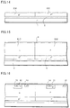
- Fig. 13 shows a sectional view of a conventional typical semiconductor integrated circuit device (e.g. Japanese Patent Publication No. 11-354535). Now referring to Figs. 14-20, an explanation will be given of a method for manufacturing the semiconductor integrated circuit device shown in Fig. 13.
- a conventional typical semiconductor integrated circuit device e.g. Japanese Patent Publication No. 11-354535.
- Fig. 14 shows an area where a high voltage vertical NPN vertical transistor is to be formed and another area where a high voltage vertical PNP transistor is to be formed.
- a buried oxide film 2 having a thickness of about 2 ⁇ m is formed on the surface of an N type substrate 3 of Si by thermal oxidation.
- the N type substrate is bonded to a supporting substrate 1 through the buried oxide film 2 at room temperature.
- the N type substrate 3 will be changed into an N + type buried layer 4 and a P + type buried layer 5, which are active layers, by the subsequent step.
- the N type substrate 3 may be a silicon substrate having e.g. resistivity of about 10 ⁇ cm.
- the substrate 3 is annealed in an atmosphere of oxygen e.g.
- the thickness of the N type substrate 3 is reduced to a prescribed thickness, e.g. 2 ⁇ m by e.g. mechanical polishing or chemical-mechanical polishing (CMP).
- CMP chemical-mechanical polishing
- N + buried layer 4 is formed in order to form an N + buried layer 4.
- N type impurities of e.g. arsenic (As) are ion-implanted at an accelerating voltage of 50 keV and dose of 3x10 15 /cm 2 . Thereafter, the photoresist is removed. Further ion-implantation is executed to form a P + type buried layer 5.
- P type impurities of e.g. boron (B) are ion-implanted at an accelerating voltage of 50 keV and dose of 3x10 15 /cm 2 . Thereafter, the photoresist is removed.
- the substrate is annealed in an atmosphere of water vapor e.g. for about one hour at 1100 °C so that the arsenic introduced in the NPN transistor section and boron introduced in the PNP transistor section in the previous step are thermally diffused, respectively, thereby forming the N + type buried layer 4 and the P + type buried layer 5.
- an oxide layer (not shown) is formed on the surface of the active layer. So, this oxide layer is removed by light etching using e.g. a hydrofluoric acid solution, which results in a structure as shown in Fig. 14.
- an N type epitaxial layer 6 having resistively of 10 ⁇ cm and a film thickness of 15 ⁇ m is grown on the N + type buried layer 4 and the P + type buried layer 5 which are the active layers.
- the NPN transistor section of the N type epitaxial layer 6 constitutes an N type collector region 7, whereas the PNP transistor section of the N type epitaxial layer 6 is changed into a P type collector region 8 by the subsequent step.
- an oxide film 9 having a thickness of 50 nm is formed by thermal oxidation.
- boron (B) are ion-implanted at an accelerating voltage of 300 keV and dose of 8x10 12 /cm 2 .
- the substrate is annealed in an atmosphere of inert gas for e.g. 7 (seven) hours at 1200 °C to form the P type collector region 8 of the PNP transistor, which results in a structure as shown in Fig. 15.
- P type impurities of e.g. boron (B) are ion-implanted at an accelerating voltage of 40 keV and dose of 1x10 14 /cm 2 .
- N type impurities of e.g. phosphorous (P) are ion-implanted at an accelerating voltage of 60 keV and dose of 1x10 14 /cm 2 .
- the substrate is annealed in an atmosphere of inert gas for e.g. 30 minutes at 900 °C.
- the impurities are thermally diffused to form a P type base region 10 of the NPN transistor and an N type base region 11 of the NPN transistor, respectively.
- N type impurities e.g. arsenic (As) are ion-implanted at an accelerating voltage of 110 keV and dose of 5x10 15 /cm 2 . Thereafter, the photoresist is removed. Subsequently, by known photolithography, using as a mask photoresist with openings on a P type emitter region and a P type collector contact of the PNP transistor, P type impurities of e.g.
- boron (B) are ion-implanted at an accelerating voltage of 40 keV and dose of 3x10 15 /cm 2 .
- the substrate is annealed in an atmosphere of inert gas for e.g. about 30 minutes at 1000°C.
- the impurities are thermally diffused to form an N + type emitter region 12 and an N + type collector contact 13 of the NPN transistor, and a P + type emitter region 14 and P + type collector contact 15 of the PNP transistor, respectively.
- the structure as shown in Fig. 16 results.
- the oxide layer 9, N type collector layer and N + type buried layer 4 of the NPN transistor section are etched to reach the buried oxide layer 2, thereby forming a trench 16 for element isolation.
- the oxide layer 9, P type collector layer 8 and P type buried layer 5 of the PNP transistor section are etched to reach the buried oxide layer 2, thereby forming a trench 16 for element isolation.
- the trenches 16 are formed so that the sides of the collector contacts 13 and 15 are exposed within the trenches 16, respectively.
- an oxide film 17 having a thickness of about 500 nm is formed on the inner wall of the trench 16. Further, the oxide film 17 abutting on the collector contacts 13 and 15 of the NPN transistor and PNP transistor is removed by etching. Thus, the structure as shown in Fig. 18 results.
- CVD Chemical Vapor Deposition
- poly-Si 18 is deposited to be buried within the trench 16 with the oxide film 17. Thereafter, the poly-Si 18 which has overflowed is etched back by Reactive Ion Etching (RIE) to flatten the substrate surface.
- RIE Reactive Ion Etching
- N type impurities are introduced into the poly-Si 18 buried in the trench 16 which abuts on the N + type collector contact 13 of the NPN transistor.
- N type impurities of e.g. phosphorous (P) are ion-implanted at an accelerating voltage 180 keV and dose of 5x10 15 /cm 2 .
- P type impurities are introduced into the poly-Si 18 buried in the trench 16 which abuts on the P + type collector contact 15 of the PNP transistor.
- P type impurities of e.g. boron (B) are ion-implanted at an accelerating voltage of 180 keV and dose of 5x10 15 /cm 2 .
- the substrate is annealed in an atmosphere of inert gas for e.g. about 30 minutes at 1000 °C.
- the phosphorous (P) is thermally diffused from the trench of the NPN transistor, thereby forming an N + type diffused layer 18n which connects the N+ type buried layer 4 and the N+ type collector contact 13.
- boron (B) is thermally diffused from the trench of the PNP transistor, thereby forming a P + type diffused layer 18p which connects the P + buried layer 5 and the P + type collector contact 15.
- the impurities are diffused from the poly-Si within the trench into the monocrystal Si (epitaxial layer) of the collector region in a short time.
- the impurities which have moved into the collector region are diffused at the same speed as that in the monocrystal Si and accumulated in a layer at the interface between the trench and the collector region, thereby forming N + type diffused layer 18n and the P + type diffused layer 18p (collector walls) .
- the structure as shown in Fig. 20 results.
- an oxide film 19 is deposited on the entire surface of the substrate.
- photoresist is deposited on the entire surface, and by known photolithography, openings are made at the positions where electrode are to be formed.
- the photoresist as a mask, by e.g. RIE, the openings are made in the oxide film 19 and the portions thereof where the electrodes are to be formed.
- aluminum (Al) 20 is deposited on the entire surface of the oxide film 19 with the openings at the portions where the electrodes are to be formed.
- photoresist is deposited on the entire surface, and by known photolithography, the photoresist is removed at the other portions than the portions where the electrodes are to be formed. Using the remaining photoresist as a mask, bye.g. RIE, the aluminum 20 is patterned. By removing the photoresist after the electrodes have been formed, the semiconductor device whose section is shown in Fig. 13 results.
- the NPN transistor and PNP transistor which are adjacent to each other are electrically isolated by the dielectricisolationtechnique.
- the degreeofintegration is enhanced, and the parasitic capacitance of the PN junction in each transistor can be reduced. This contribute to the high speed operation of the device.
- the base-collector withstand voltage is assured by reducing the impurity concentration in the collector region 7, 8.
- reduction in the impurity concentration in the entire collector regions 7, 8 increases the series resistance of the collector, thus deteriorating the characteristic.
- the collector walls N + diffused layer 18n, P + diffused layer 18p are formed which connect the highly doped buried layers 4, 5 and the collector contacts 13, 15, respectively. In this way, the high withstand voltage of the bipolar transistor can be realized while the high speed operation which is a benefit of the bipolar transistor is utilized.
- the lightly-doped collector regions 7 and 8, i.e. N type epitaxial layer 6 must be formed be thick in order to realize a high withstand voltage.
- heat treatment for a long time at a high temperature is required so that making the thick film of the collector regions has a limitation in process. Therefore, the film thickness of the collector regions formed of a single epitaxial layer has a limitation to realize the high withstand voltage. Accordingly, the conventional semiconductor integrated circuit could not provide a necessary withstand voltage.
- the conventional method of manufacturing a semiconductor integrated circuit device in order to realize a dielectric-isolated complementary transistor pair composed of an NPN transistor and a vertical PNP transistor which are formed to be adjacent to each other on a single chip, a trench was used to isolate both transistors from each other.
- the trench has a limitation in depth and imperfection in an etching accuracy. Therefore, the conventional method has a problem that the etching for element isolation, attended with the thick film of the epitaxial layer for realizing the high withstand voltage, is difficult.
- the lightly-doped collector regions'7 and 8 i.e. N type epitaxial layer 6 are made thick in order to realize the high withstand voltage
- the lightly-doped collector region 8 of the vertical PNP transistor must be formed in such a manner that the ion-implanted impurities are heat treated for a long time at a high temperature. Therefore, the formation of the thick film of the N type epitaxial layer has a limitation in process, and increase the production cost. Further, ion-implanting at a high accelerating voltage and high dose for the purpose of increasing the depth of the impurity diffusion disadvantageously makes the crystal defect of the Si substrate remarkable.
- a method for manufacturing a semiconductor integrated circuit device comprising: a step of preparing one conductive semiconductor substrate; a step of forming plural opposite conductive epitaxial layers on said substrate, diffusing the one conductive and the opposite conductive buried layers formed on said substrate and said epitaxial layers to connect, and forming a first and second buried layers consisting of high concentration impurity diffusing layer at a first and second island regions and periphery of the first and second islands region; a step of etching the both end portions of said first and second island regions in V groove shape remaining said first and second buried layers, a step of forming an oxide film on the surface of said first and second buried layers and forming a polycrystal semiconductor layer on the oxide film; a step of forming an oxide film on said polycrystal semiconductor layer and bonding a supporting substrate through the oxide film; and a step of polishing said semiconductor substrate setting said supporting substrate to the bottom face till said first and second island regions are exposed.
- process etching said first and second island regions is suitably a process etching in V groove in order to remove completely the border face between said buried layer consisting of low concentration impurity diffusing layer forming said first and second island regions and said epitaxial layer, to etch completely to the bottom portion of said first and second island regions made thick in film, and to realize dielectric-isolated complementary bipolar transistors.
- the buried layer comprising high concentration impurity diffusing layer formed at periphery of the collector region is suitably formed at the same time forming the buried layer forming the collector region, and along inclined lines of V groove etching.
- high concentration buried layer too is formed at the same time by process of V groove etching isolating elements between said first and second island regions so as to shorten manufacturing process of the semiconductor integrated circuit device.
- generation of crystal defect at the substrate can be clearly decreased comparing with a forming collector taking-out diffusion layer ion-injecting on surface of the substrate because ion injection is carried out on surface of the epitaxial layer.
- Fig. 1 is a sectional view of a first embodiment of an IC according to this invention in which a high voltage NPN transistor 21 and a high voltage vertical PNP transistor 22 are formed through poly-Si 59 as dielectric-isolated complementary bipolar transistors.
- poly-Si 59 is formed on a supporting substrate 61 covered with a silicon oxide film 60.
- the supporting substrate 61 is bonded to the poly-Si 59 through the silicon oxide film 60 by heat treatment for about two hours at 1100°C - 1200°C.
- the dielectric-isolated complementary bipolar transistors are formed through the poly-Si 59.
- a silicon oxide film 58 and a N + type buried layer 55 are formed to surround a collector 54.
- the collector region 54 includes an N + type diffused region 64 serving as a collector taking-out region, a P type diffused region 62 serving as a base region and an N + type diffused layer 66 serving as an emitter region.
- the collector taking-out region 64 which is coupled with the N + buried region 55, constitutes an N + highly doped layer, thus realizing a structure with a reduced collector resistance of the high voltage NPN transistor 21.
- a silicon oxide film 58 and a P + buried layer 57 are formed to surround a collector region 56.
- the collector region 56 includes a P + type region 65 serving as a collector taking-out region, an N + type well region 63 serving as a base region and a P + type diffused region 67 serving as an emitter region.
- the collector taking-out region 65 which is coupled with the P + buried region 57, constitutes a P + highly doped layer, thus realizing a structure with a reduced collector resistance of the high voltage PNP transistor 22.
- electrode wirings of Al, interlayer insulating film of polyimide insulating film and a polyimide jacket coating, etc. are formed on these elements.
- the N + type and P + type buried layers 55 and 57 which are formed on the periphery of the N - type and P - type collector regions 54 and 56, respectively, are coupled with the collector taking-out regions 64 and 65, respectively.
- This provides the N + type and P + type highly-doped layers to reduce the collector resistance so that the collector regions 54 and 56 can be made thick.
- the high voltage complementary bipolar transistors can be formed.
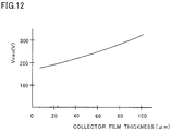
- Fig. 13 shows a relationship between a collector region film thickness and a withstand voltage in the dielectric-isolated complementary transistors in the semiconductor integrated circuit device according to this invention.
- the collector-emitter withstand voltage of 300 V can be obtained so that the high voltage complementary bipolar transistors can be formed.
- the film thickness of about 60 ⁇ m or larger is required. This film thickness far exceeds the limitation in the manufacturing method using a trench.
- the NPN transistor 21 and PNP transistor 22 are surely dielectric-isolated through the poly-Si 59. For this reason, influence of the transistors 21 and 22 from each other and creation of the parasitic transistor can be suppressed so that the semiconductor integrated circuit device is more suitable for a high frequency operation.
- a P type monocrystal Si substrate 23 of a crystal axis of (100) has a resistivity of at least 50 ⁇ cm.
- An epitaxial layer is stacked on the substrate 23 to form an area where transistors are to be formed.
- multiple epitaxial layers are stacked.
- the substrate 23 is placed at a high temperature for a long time.
- the substrate is placed at about 1000 - 1400°C for 24 hours.
- the epitaxial layer which is used as the collector regions 54 and 56 can be made thick, thereby permitting a high voltage transistor to be realized.
- a P type monocrystal silicon substrate 23 of about 650 ⁇ m thickness is prepared, and oxide film is formed by thermal oxidation of surface of the substrate 23 so that a selecting mask is made by photo-etching the oxide film.
- Phosphorus (P) forming N - first buried layer 24 and N + first buried layers 25 and 26, and boron (B) forming P - first buried layer 27 and P + first buried layers 28 and 29 are ion-implanted and diffused in the surface of the substrate 23.
- the substrate 23 is arranged on a suscepter of an epitaxial growing apparatus, and N or N - first epitaxial layer 30 grows 18 to 22 ⁇ m by applying high temperature of 1140 °C to the substrate leading SiH 2 Cl 2 gas and H 2 gas into reactant tube.
- Oxide film is formed by thermal oxidation of surface of first epitaxial layer 30, each selecting mask is made by photo-etching the oxide film.
- Phosphorus (P) forming N - second buried layer 31 and N + second buried layers 32 and 33, and boron (B) forming P - second buried layer 34 and P + second buried layers 35 and 36 are ion-implanted and diffused in the surface of the first epitaxial layer 30.
- the substrate 23 is arranged on a suscepter of an epitaxial growing device, and N or N - first epitaxial layer 37 grows 18 to 22 ⁇ m by applying high temperature of 1140 °C to the substrate leading SiH 2 Cl 2 gas and H 2 gas into reactant tube.
- Oxide film is formed by thermal oxidation of surface of second epitaxial layer 37, each selecting mask is made by photo-etching the oxide film.
- Phosphorus (P) forming N - third buried layer 38 and N + third buried layers 39 and 40, and boron (B) forming P - third buried layer 41 and P + second buried layers 42 and 43 are ion-implanted and diffused in the surface of the second epitaxial layer 37.
- the N - first and second buried layers 24 and 31, the N + first and second buried layers 25, 26, 32, and 33, the P - first and second buried layers 27 and 34, the P + first and second buried layers 28, 29, 35, and 36 are diffused to connect.
- the substrate 23 is arranged on a suscepter of an epitaxial growing device, and N or N - third epitaxial layer 44 grows 18 to 22 ⁇ m by applying high temperature of 1140 °C to the substrate leading SiH 2 Cl 2 gas and H 2 gas into reactant tube.
- Oxide film is formed by thermal oxidation of surface of third epitaxial layer 44, each selecting mask is made by photo-etching the oxide film.
- Phosphorus (P) forming N - fourth buried layer 45 and N + fourth buried layers 46 and 47, and boron (B) forming P - fourth buried layer 48 and P + second buried layers 49 and 50 are ion-implanted and diffused in the surface of the third epitaxial layer 44.
- the N - second and third buried layers 31 and 38, the N + second and third buried layers 32, 33, 39, and 40, the P - second and third buried layers 34, and 41, the P + second and third buried layers 35, 36, 42, and 43 are diffused to connect.
- the substrate 23 is arranged on a suscepter of an epitaxial growing device, and N or N - fourth epitaxial layer 51 grows 18 to 22 ⁇ m by applying high temperature of 1140 °C to the substrate leading SiH 2 Cl 2 gas and H 2 gas into reactant tube.
- Phosphorus (P) forming N + fifth buried layer 52 and boron (B) forming P + fifth buried layer 53 are ion-implanted and diffused in the surface of the fourth epitaxial layer 51.
- width of the N + fifth buried layer 52 and the P + fifth buried layer 53 is formed to almost similar width of the N - fourth buried layer 45, the N + fourth buried layers 46 and 47, the P - fourth buried layer 48, the P + second buried layers 49 and 50 formed on the third epitaxial layer 44.
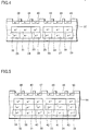
- region forming the N - collector region 54 of the NPN transistor 21, the N + buried layer 55, the P - collector region 56 of the PNP transistor 22, and the P + buried layer 57 is obtained as shown in the figure.
- phosphorous (P) is used as N type impurities and boron (B) is used as P type impurities because the impurities having a high diffusing speed assures the coupling the buried layers for a short heat treating time. Namely, this intends to form a flat profile in a short time in the N type impurity region and P type impurity region.
- This invention is also characterized in that the regions where the NPN transistor 21 and PNP transistor 22 are to be formed can be formed simultaneously on the substrate 23.
- oxide film is formed by thermal oxidation of surface the fourth epitaxial layer 51 and a selecting mask is made by photoetching the oxide film as shown in Fig. 7.
- a selecting mask is made by photoetching the oxide film as shown in Fig. 7.
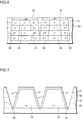
- V grooves for element isolation are formed.
- deposition with CVD is carried out so as to make polycristal silicon 59 about 150 ⁇ m in high temperature, about 1240 °C, for about one hour on a silicon oxide film 58.
- the polycristal silicon 59 is flattened by polishing so that even thin part of film thickness is about 30 ⁇ m, a supporting substrate 61 is surely bonded by heat treatment of 1100 to 1200 °C, for about 2 hours bonding the supporting substrate 61 on surface of the polycristal silicon 59 preparing individually wafer coating a silicon film 60.
- the supporting substrate 61 may be material enabling to resist polishing process of the next process and is not need conductive material.
- the substrate is turned upside down so that the monocrystal Si substrate 23 constitutes an upper surface and the supporting substrate 61 constitutes a bottom surface.
- the silicon substrate 23 is polished about 580 ⁇ m till the N - collector region 54 and the P - collector region 56 expose from surface of the silicon substrate 23.
- the N - collector region 54 and the P - collector region 56 become a structure dielectric-isolated through the polycrystal silicon 59.
- the N - collector region 54 and the P - collector region 56 are formed in film thickness of about 60 to 80 ⁇ m.
- a P type diffused region 62 is formed as a base region in the N - type collector region 54, and a N + type well region 63 is formed as a base region in the P - type collector region 56.
- the surface of the N - type collector region 54 and P - type collector region 56 are thermally oxidized to form an oxide film.
- the oxide film is photo-etched to provide a selective mask.
- Arsenic (As) is ion-implanted and diffused in the N - type collector region 54 to provide an N + diffused region 64 serving as a collector taking-out region
- boron (B) is ion-implanted and diffused in the P - type collector region 56 to provide a P + type diffused region 65 serving as a collector taking-out region.
- an N + type diffused region 66 is formed as an emitter region in the P type diffused region 62 to make an NPN transistor 21.
- a P + type diffused region 67 is formed as an emitter region in the N + type well region 63 to make a PNP transistor 22.
- the N + type collector taking-out region 64 and P + collector taking-out region 65 can be coupled with the N + type buried layer 55 and the P + type buried layer 57 in a short diffusion time, respectively.
- the N + type collector taking-out region 64 and the P + type collector taking-out region 65 are coupled with the N + buried layer 55 and the P + type buried layer 57, respectively to constitute a structure with reduced collector resistance.
- the buried layer can be formed for all epitaxial layers using the same masks . This is an economical method for manufacturing as one mask is used.
- high concentration layer region is formed and collector resistance is decreased by forming the buried layer of high concentration layer and connecting with the high concentration collector taking-out region, and the thick collector region is realized so as to realize a semiconductor integrated circuit device superior in high voltage resistance in the semiconductor integrated circuit device.
- making the collector region thick is realized so as to realize a method for manufacturing a semiconductor integrated circuit device superior in high voltage resistance because many layers of the epitaxial layer are formed at process of forming the collector region.
- accurate etching can be carried out to deep portion by etching of V groove shape at process of etching the collector region, and dielectric is surely isolated by polycrystal silicon so as to realize a method for manufacturing a semiconductor integrated circuit device decreasing influence of mutual transistors.
- the collector region and the collector taking-out region are formed at one time by forming the same process as the buried layer forming the collector region and the buried layer forming the collector taking-out region so as to realize a method for manufacturing a semiconductor integrated circuit device very superior in productivity.
- the high concentration buried layer is formed with incline by etching of V groove. Therefore, the collector taking-out region is connected to high concentration buried layer without almost diffusing the collector region, and is formed by the same process as the emitter region so as to realize a method for manufacturing a semiconductor integrated circuit device very superior in productivity.
Landscapes
- Bipolar Transistors (AREA)
- Bipolar Integrated Circuits (AREA)
- Element Separation (AREA)
- Mechanical Treatment Of Semiconductor (AREA)
Abstract
Description
Claims (5)
- A method for manufacturing a semiconductor integrated circuit device comprising steps of:preparing a semiconductor substrate having one conduction type;forming plural epitaxial layers having opposite conduction type on said substrate, diffusing the one conductive and an opposite conductive buried layers formed on said substrate and said epitaxial layers to connect, and forming a first and second buried layers of highly-doped impurity diffused layer at a first and second islands regions and periphery of the first and second islands regions;etching the both ends portions of said first and second island regions in V-groove remaining said first and second buried layers;forming a polycrystal semiconductor layer on the oxide film and forming an oxide film on the surface of said first and second buried layers;forming an oxide film on said polycrystal semiconductor layer and bonding a supporting substrate through the oxide film; andpolishing said semiconductor substrate with said supporting substrate located down, until said first and second island regions are exposed.
- A method for manufacturing a semiconductor integrated circuit device according to claim 1, wherein said first and second buried layers of highly-doped impurity diffused layer are formed along inclined lines of said V groove etching.
- A method for manufacturing a semiconductor integrated circuit device according to claim 1 or 2, wherein the first and second island regions and said first and second buried layers are formed by the same process.
- A method for manufacturing a semiconductor integrated circuit device according to claim 1, 2 or 3, wherein the buried layers forming the top of said first and second island regions of highly-doped impurity diffused layers.
- A method for manufacturing a semiconductor integrated circuit device according to claim 1, 2, 3 or 4, wherein the transistors different in conductive type are formed at said first and second island regions exposed.
Applications Claiming Priority (2)
| Application Number | Priority Date | Filing Date | Title |
|---|---|---|---|
| JP2000271381A JP2002083876A (en) | 2000-09-07 | 2000-09-07 | Method for manufacturing semiconductor integrated circuit device |
| JP2000271381 | 2000-09-07 |
Publications (3)
| Publication Number | Publication Date |
|---|---|
| EP1187194A2 true EP1187194A2 (en) | 2002-03-13 |
| EP1187194A3 EP1187194A3 (en) | 2004-11-10 |
| EP1187194B1 EP1187194B1 (en) | 2007-03-07 |
Family
ID=18757679
Family Applications (1)
| Application Number | Title | Priority Date | Filing Date |
|---|---|---|---|
| EP01307575A Expired - Lifetime EP1187194B1 (en) | 2000-09-07 | 2001-09-06 | Method for manufacturing semiconductor integrated circuit device |
Country Status (7)
| Country | Link |
|---|---|
| US (1) | US6528379B2 (en) |
| EP (1) | EP1187194B1 (en) |
| JP (1) | JP2002083876A (en) |
| KR (1) | KR100582146B1 (en) |
| CN (1) | CN1213474C (en) |
| DE (1) | DE60127052T2 (en) |
| TW (1) | TW503572B (en) |
Cited By (1)
| Publication number | Priority date | Publication date | Assignee | Title |
|---|---|---|---|---|
| CN100457674C (en) * | 2006-12-02 | 2009-02-04 | 桂林工学院 | Fly ash red sandstone sintered building brick and its preparation technology |
Families Citing this family (12)
| Publication number | Priority date | Publication date | Assignee | Title |
|---|---|---|---|---|
| KR100854077B1 (en) * | 2002-05-28 | 2008-08-25 | 페어차일드코리아반도체 주식회사 | SOI substrate manufacturing method using wafer bonding and complementary high voltage bipolar transistor manufacturing method using SOI substrate |
| KR100477396B1 (en) * | 2002-09-04 | 2005-03-28 | 한국전기연구원 | SiC MOSFET devices having metal gate electrode and manufacturing method thereof |
| KR100474859B1 (en) * | 2002-11-05 | 2005-03-11 | 매그나칩 반도체 유한회사 | Method of forming an isolation layer in a semiconductor device |
| JP2006270009A (en) * | 2005-02-25 | 2006-10-05 | Seiko Epson Corp | Manufacturing method of electronic device |
| JP6084226B2 (en) * | 2011-10-14 | 2017-02-22 | ディフテック レーザーズ インコーポレイテッド | Planarized semiconductor particles positioned on a substrate |
| US9455307B2 (en) | 2011-10-14 | 2016-09-27 | Diftek Lasers, Inc. | Active matrix electro-optical device and method of making thereof |
| US9209019B2 (en) | 2013-09-05 | 2015-12-08 | Diftek Lasers, Inc. | Method and system for manufacturing a semi-conducting backplane |
| US10312310B2 (en) | 2016-01-19 | 2019-06-04 | Diftek Lasers, Inc. | OLED display and method of fabrication thereof |
| CN109643729B (en) * | 2016-09-01 | 2022-03-29 | 美国亚德诺半导体公司 | Low capacitance switch for PGA or PGIA |
| US10707330B2 (en) | 2018-02-15 | 2020-07-07 | Globalfoundries Inc. | Semiconductor device with interconnect to source/drain |
| CN110544689B (en) * | 2019-08-29 | 2021-07-20 | 华南理工大学 | Active device and passive single crystal device and monolithic integration method in radio frequency front-end module |
| EP4002503B1 (en) * | 2020-11-23 | 2024-04-17 | Melexis Technologies SA | Semiconductor device with integrated magnetic flux concentrator, and method for producing same |
Family Cites Families (6)
| Publication number | Priority date | Publication date | Assignee | Title |
|---|---|---|---|---|
| US4146905A (en) * | 1974-06-18 | 1979-03-27 | U.S. Philips Corporation | Semiconductor device having complementary transistor structures and method of manufacturing same |
| GB2060252B (en) * | 1979-09-17 | 1984-02-22 | Nippon Telegraph & Telephone | Mutually isolated complementary semiconductor elements |
| JPS56131942A (en) * | 1980-03-19 | 1981-10-15 | Fujitsu Ltd | Manufacture of semiconductor device |
| JPS6081839A (en) * | 1983-10-12 | 1985-05-09 | Fujitsu Ltd | Manufacture of semiconductor device |
| JPH0783050B2 (en) * | 1985-06-21 | 1995-09-06 | 株式会社東芝 | Method for manufacturing semiconductor device |
| JPH11354535A (en) | 1998-06-11 | 1999-12-24 | Sony Corp | Semiconductor device and manufacturing method thereof |
-
2000
- 2000-09-07 JP JP2000271381A patent/JP2002083876A/en active Pending
-
2001
- 2001-08-28 TW TW090121120A patent/TW503572B/en not_active IP Right Cessation
- 2001-09-05 US US09/946,948 patent/US6528379B2/en not_active Expired - Fee Related
- 2001-09-06 DE DE60127052T patent/DE60127052T2/en not_active Expired - Fee Related
- 2001-09-06 EP EP01307575A patent/EP1187194B1/en not_active Expired - Lifetime
- 2001-09-06 KR KR1020010054628A patent/KR100582146B1/en not_active Expired - Fee Related
- 2001-09-07 CN CNB011357231A patent/CN1213474C/en not_active Expired - Fee Related
Cited By (1)
| Publication number | Priority date | Publication date | Assignee | Title |
|---|---|---|---|---|
| CN100457674C (en) * | 2006-12-02 | 2009-02-04 | 桂林工学院 | Fly ash red sandstone sintered building brick and its preparation technology |
Also Published As
| Publication number | Publication date |
|---|---|
| CN1341961A (en) | 2002-03-27 |
| US20020028551A1 (en) | 2002-03-07 |
| DE60127052T2 (en) | 2007-12-13 |
| KR20020020215A (en) | 2002-03-14 |
| CN1213474C (en) | 2005-08-03 |
| JP2002083876A (en) | 2002-03-22 |
| DE60127052D1 (en) | 2007-04-19 |
| KR100582146B1 (en) | 2006-05-23 |
| EP1187194B1 (en) | 2007-03-07 |
| TW503572B (en) | 2002-09-21 |
| EP1187194A3 (en) | 2004-11-10 |
| US6528379B2 (en) | 2003-03-04 |
Similar Documents
| Publication | Publication Date | Title |
|---|---|---|
| US4897362A (en) | Double epitaxial method of fabricating semiconductor devices on bonded wafers | |
| EP1187194B1 (en) | Method for manufacturing semiconductor integrated circuit device | |
| JPH10256270A (en) | Complementary bipolar transistor and method of manufacturing the same | |
| JPH0793315B2 (en) | Semiconductor device and manufacturing method thereof | |
| KR940009361B1 (en) | Hybrid Integrated Circuit Devices | |
| JPH03178133A (en) | Bipolar transistor and its fabrication method | |
| JP2587444B2 (en) | Bipolar transistor using CMOS technology and method of manufacturing the same | |
| KR19980071857A (en) | Bipolar transistor on insulator semiconductor substrate and manufacturing method thereof | |
| US6545337B2 (en) | Semiconductor integrated circuit device | |
| US5763931A (en) | Semiconductor device with SOI structure and fabrication method thereof | |
| JPH11354535A (en) | Semiconductor device and manufacturing method thereof | |
| US5843828A (en) | Method for fabricating a semiconductor device with bipolar transistor | |
| JP2002083877A (en) | Semiconductor integrated circuit device and method of manufacturing the same | |
| US7101750B2 (en) | Semiconductor device for integrated injection logic cell and process for fabricating the same | |
| JP5238941B2 (en) | Manufacturing method of semiconductor device | |
| JPS61172346A (en) | Semiconductor integrated circuit device | |
| JP3707978B2 (en) | Semiconductor integrated circuit and manufacturing method thereof | |
| JP2003258216A (en) | Method for manufacturing optical semiconductor integrated circuit device | |
| JP2002083875A (en) | Method for manufacturing semiconductor integrated circuit device | |
| JPH0421343B2 (en) | ||
| JP3130330B2 (en) | Manufacturing method of semiconductor integrated circuit | |
| JPS6239538B2 (en) | ||
| JP2002083817A (en) | Semiconductor device and manufacturing method thereof | |
| JPH0817181B2 (en) | Semiconductor device and manufacturing method thereof | |
| KR20000051282A (en) | Manufacturing Method for Semiconductor Device |
Legal Events
| Date | Code | Title | Description |
|---|---|---|---|
| PUAI | Public reference made under article 153(3) epc to a published international application that has entered the european phase |
Free format text: ORIGINAL CODE: 0009012 |
|
| AK | Designated contracting states |
Kind code of ref document: A2 Designated state(s): AT BE CH CY DE DK ES FI FR GB GR IE IT LI LU MC NL PT SE TR |
|
| AX | Request for extension of the european patent |
Free format text: AL;LT;LV;MK;RO;SI |
|
| PUAL | Search report despatched |
Free format text: ORIGINAL CODE: 0009013 |
|
| AK | Designated contracting states |
Kind code of ref document: A3 Designated state(s): AT BE CH CY DE DK ES FI FR GB GR IE IT LI LU MC NL PT SE TR |
|
| AX | Request for extension of the european patent |
Extension state: AL LT LV MK RO SI |
|
| 17P | Request for examination filed |
Effective date: 20050125 |
|
| AKX | Designation fees paid |
Designated state(s): DE FR GB |
|
| 17Q | First examination report despatched |
Effective date: 20050627 |
|
| GRAP | Despatch of communication of intention to grant a patent |
Free format text: ORIGINAL CODE: EPIDOSNIGR1 |
|
| GRAS | Grant fee paid |
Free format text: ORIGINAL CODE: EPIDOSNIGR3 |
|
| GRAA | (expected) grant |
Free format text: ORIGINAL CODE: 0009210 |
|
| AK | Designated contracting states |
Kind code of ref document: B1 Designated state(s): DE FR GB |
|
| REG | Reference to a national code |
Ref country code: GB Ref legal event code: FG4D |
|
| REF | Corresponds to: |
Ref document number: 60127052 Country of ref document: DE Date of ref document: 20070419 Kind code of ref document: P |
|
| PGFP | Annual fee paid to national office [announced via postgrant information from national office to epo] |
Ref country code: DE Payment date: 20070830 Year of fee payment: 7 |
|
| PGFP | Annual fee paid to national office [announced via postgrant information from national office to epo] |
Ref country code: GB Payment date: 20070905 Year of fee payment: 7 |
|
| PLBE | No opposition filed within time limit |
Free format text: ORIGINAL CODE: 0009261 |
|
| STAA | Information on the status of an ep patent application or granted ep patent |
Free format text: STATUS: NO OPPOSITION FILED WITHIN TIME LIMIT |
|
| 26N | No opposition filed |
Effective date: 20071210 |
|
| PGFP | Annual fee paid to national office [announced via postgrant information from national office to epo] |
Ref country code: FR Payment date: 20070914 Year of fee payment: 7 |
|
| GBPC | Gb: european patent ceased through non-payment of renewal fee |
Effective date: 20080906 |
|
| REG | Reference to a national code |
Ref country code: FR Ref legal event code: ST Effective date: 20090529 |
|
| PG25 | Lapsed in a contracting state [announced via postgrant information from national office to epo] |
Ref country code: DE Free format text: LAPSE BECAUSE OF NON-PAYMENT OF DUE FEES Effective date: 20090401 |
|
| PG25 | Lapsed in a contracting state [announced via postgrant information from national office to epo] |
Ref country code: FR Free format text: LAPSE BECAUSE OF NON-PAYMENT OF DUE FEES Effective date: 20080930 |
|
| PG25 | Lapsed in a contracting state [announced via postgrant information from national office to epo] |
Ref country code: GB Free format text: LAPSE BECAUSE OF NON-PAYMENT OF DUE FEES Effective date: 20080906 |