EP1186885A1 - Field-effect transistor - Google Patents
Field-effect transistor Download PDFInfo
- Publication number
- EP1186885A1 EP1186885A1 EP01915765A EP01915765A EP1186885A1 EP 1186885 A1 EP1186885 A1 EP 1186885A1 EP 01915765 A EP01915765 A EP 01915765A EP 01915765 A EP01915765 A EP 01915765A EP 1186885 A1 EP1186885 A1 EP 1186885A1
- Authority
- EP
- European Patent Office
- Prior art keywords
- effect transistor
- field effect
- diamond
- fet
- gate
- Prior art date
- Legal status (The legal status is an assumption and is not a legal conclusion. Google has not performed a legal analysis and makes no representation as to the accuracy of the status listed.)
- Granted
Links
Images





Classifications
-
- G—PHYSICS
- G01—MEASURING; TESTING
- G01N—INVESTIGATING OR ANALYSING MATERIALS BY DETERMINING THEIR CHEMICAL OR PHYSICAL PROPERTIES
- G01N27/00—Investigating or analysing materials by the use of electric, electrochemical, or magnetic means
- G01N27/26—Investigating or analysing materials by the use of electric, electrochemical, or magnetic means by investigating electrochemical variables; by using electrolysis or electrophoresis
- G01N27/403—Cells and electrode assemblies
- G01N27/414—Ion-sensitive or chemical field-effect transistors, i.e. ISFETS or CHEMFETS
-
- H—ELECTRICITY
- H10—SEMICONDUCTOR DEVICES; ELECTRIC SOLID-STATE DEVICES NOT OTHERWISE PROVIDED FOR
- H10W—GENERIC PACKAGES, INTERCONNECTIONS, CONNECTORS OR OTHER CONSTRUCTIONAL DETAILS OF DEVICES COVERED BY CLASS H10
- H10W72/00—Interconnections or connectors in packages
- H10W72/01—Manufacture or treatment
- H10W72/015—Manufacture or treatment of bond wires
- H10W72/01515—Forming coatings
-
- H—ELECTRICITY
- H10—SEMICONDUCTOR DEVICES; ELECTRIC SOLID-STATE DEVICES NOT OTHERWISE PROVIDED FOR
- H10W—GENERIC PACKAGES, INTERCONNECTIONS, CONNECTORS OR OTHER CONSTRUCTIONAL DETAILS OF DEVICES COVERED BY CLASS H10
- H10W72/00—Interconnections or connectors in packages
- H10W72/071—Connecting or disconnecting
- H10W72/075—Connecting or disconnecting of bond wires
Definitions
- the present invention relates to a field effect transistor which uses liquid electrolyte as a gate and a hydrogen-terminated surface of diamond as a channel.
- An undoped hydrogen-terminated diamond thin film formed by a microwave plasma CVD method has been known to have a p-type conductive layer formed on its surface, regardless of whether the diamond thin film is monocrystalline or polycrystalline.
- the present inventors have fabricated a field effect transistor (FET) in which deposition of metal or insulating substance on the gate portion is avoided through utilization of such a surface conductive layer and have tested the operation of the FET within an electrolytic aqueous solution (Ken-ichi Kitatani, et al ., Proceedings of the 46th Applied Physics Joint Lecture Meeting, 30a-P7-22 (1999) pp. 628).
- FET field effect transistor
- an electric double layer is considered to be formed at the interface between a surface conductive layer of a diamond in an electrolytic solution and the electrolyte (Takeshi Hosomi, et al ., Abstracts of the 13th Diamond Symposium Lecture Meeting, 115 (1999) pp. 36).
- the present inventors have tackled development of an ISFET biosensor in which an ion sensitive field effect transistor (ISFET) is used as a transducer, and an enzyme is used as a molecular recognizing substance, and have found that such an ISFET biosensor can be used as a micro-sensor for clinical test, industrial measurement, and environmental measurement, with possible future application to a body-embedable sensor.
- ISFET ion sensitive field effect transistor
- an ISFET biosensor has a practical problem in that even when the molecular recognizing substance functions properly and an intended molecule is selected, operation of the ISFET itself becomes unstable due to a substance invading from outside the sensor. This unstable condition is caused by a great variation in threshold voltage attributable to generation of an interface level, or presence of ions at the oxide film/Si interface, which is the most delicate portion within an Si MOSFET.
- a sensor When a sensor is used, its surface is unavoidably exposed to the atmosphere.
- a protective layer even when a protective layer is used, a considerably large number of undesired molecules or ions invade the oxide film/Si interface as compared with the case of LSIs. Therefore, creation of a chemically strong semiconductor surface is indispensable for development of ISFET biosensors.
- a hydrogen-adsorbed surface (hydrogen-terminated surface) of diamond is stable up to 700°C in vacuum, and up to 300°C in the atmosphere; is chemically inert even in liquid; and, near room temperature, does not cause structure change even when exposed to strong acid or strong alkali.
- a p-type conductive layer is formed in the vicinity of the hydrogen-terminated diamond surface.
- the present inventors have developed an FET in which a liquid electrolyte is used as a gate.
- an object of the present invention is to provide a field effect transistor which uses a liquid electrolyte as a gate and which operates stably in the liquid electrolyte.
- the present invention provides the following.
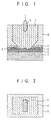
- FIG. 1 is a cross-sectional view of a liquid-electrolyte-gate diamond FET (p-channel FET) according to the present invention
- FIG. 2 is a plan view of the FET.
- reference numeral 1 denotes a polycrystalline diamond serving as a substrate
- 2 denotes a channel (terminated surface of the polycrystalline diamond: p-type surface conductive layer)
- 3 denotes a source electrode (Au electrode);4 denotes a gate (liquid electrolyte: e.g., KOH aqueous solution);
- 5 denotes a gate electrode;
- 6 denotes a drain electrode (Au electrode); 7 denotes a protective film; and 8 denotes a liquid vessel (insulator).
- Drain current is controlled by gate voltage and can be pinched off completely.
- the threshold voltage of the FET varies within the range of ⁇ 0.2 V when pH of the liquid electrolyte varies from 1 to 14, does not show Nernst response, and exhibits almost no pH dependency.
- the operation voltage range of the FET corresponds to the range of an electric potential window in the case where diamond is used as an electrochemical electrode.
- the diamond is monocrystalline or polycrystalline, and the surface of the diamond is covered with hydrogen atoms.
- FIG. 3 shows steps of a method for fabricating the liquid-electrolyte-gate diamond FET according to a first embodiment of the present invention, wherein FIG. 3[A] shows top views of the diamond FET in the respective steps; and FIG. 3[B] shows cross-sectional views of the diamond FET in the respective steps.
- Metal is vapor-deposited all over the surface to form a metal film, and a portion of the metal film corresponding to a gate portion is removed by means of photolithography.
- Gold which forms ohmic contact with a diamond thin film, is used as the metal.
- the metal film forms pads, a source electrode, and a drain electrode.
- the gate length is set to 1 mm.
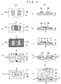
- FIG. 4 shows steps of a method for fabricating a liquid-electrolyte-gate diamond FET according to a second embodiment of the present invention, wherein FIG. 4[A] shows top views of the diamond FET in the respective steps; and FIG. 4[B] shows cross-sectional views of the diamond FET in the respective steps.
- the above described fabrication method according to the first embodiment involves troublesome work of applying resist twice, resulting in a long fabrication time.
- a metal mask is fabricated in order to eliminate necessity of etching of the gate portion.
- a molybdenum plate is used for the metal mask such that only source and drain portions are formed from the beginning.
- the gate length is reduced from 1 mm to 0.5 mm.
- the fabrication method of the present embodiment greatly simplifies the fabrication steps as compared with the case of the first fabrication method, so that the time required for fabricating an FET can be reduced to half.
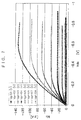
- FIGS. 5 to 7 are graphs showing static characteristics of a liquid-electrolyte-gate diamond FET fabricated according to the second embodiment of the present invention.
- the exposed gate portion was filled with an alkali aqueous solution (KOH aqueous solution); and the diamond FET was operated to obtain the static characteristics shown in FIGS. 5 to 7.
- KOH aqueous solution alkali aqueous solution
- FIG. 5 is a graph showing measurement results for the case where a pH 11 KOH aqueous solution is used;
- FIG. 6 is a graph showing measurement results for the case where a pH 9 KOH aqueous solution is used;
- FIG. 7 is a graph showing measurement results for the case where a pH 8 KOH aqueous solution is used.
- the drain current is controlled by means of a gate bias, which shows that the FET actually operates.
- This FET operates in a normally-off mode.
- the drain current is infinitesimal, and the absolute value of the drain current is seen to increase with a decrease in the absolute value of the gate bias.
- the FET is considered to be in an off mode. Static characteristics involving pinch off can be observed.
- the FET When the gate bias and the source-drain voltage were varied within the electric potential window, the FET was pinched off completely; i.e., the FET exhibited static characteristics such that saturation clearly occurred. Further, the FET was confirmed to have a constant threshold voltage of about -0.2V for the case where a pH 8 KOH was used, and was confirmed to be of a normally off type.
- FIG. 8 is a graph showing the Vg-Ids characteristics of the FET for the case where a pH 11 KOH aqueous solution is used, along with its logarithmic representation.
- FIG. 9 is a graph showing the Vg-Ids characteristics for the case where a pH 8 KOH aqueous solution is used, along with its logarithmic representation.
- the threshold voltage of the FET is -0.12V
- the threshold voltage of the FET is -0.16V.
- These threshold voltages are minus indicating a normally off type p-channel FET.
- FIG. 10 shows the relation between threshold voltage and pH in the samples (NIS03, NIS04, NIS05).
- the ratio of on-state current to off-state current of the FET was found to be slightly less than 10,000. Considering that the employed polycrystalline diamond had an uneven surface, which had not been flattened after growth, this current ratio is very high.
- a polycrystalline diamond FET having a high current ratio can be used as an FET of low power consumption.
- the present invention is expected to provide a biosensor in which the FET operates stably within a liquid electrolyte, such that a higher sensitivity can be realized by surface modification of an ion selective functional group on a channel which has no pH dependency.
- a KOH aqueous solution is used as a liquid electrolyte.
- the liquid electrolyte is not limited thereto. FET characteristics were observed for the case where other standard solutions were used, such as oxalate salt (pH 1.68), phthalate salt (pH 4), neutral phosphate salt (pH 7), borate salt (pH 9.18), and carbonate salt (pH 10.01).
- liquid vessel insulator
- a liquid electrolyte may be placed to fill the gate portions of several devices obtained at the fabrication step (d) of FIG. 3 or 4, and a common gate electrode may be disposed at an appropriate position.
- the present invention provides the following effects.
- the field effect transistor according to the present invention can effect selective detection of ions, and therefore can be applied to clinical testing, industrial measurement, and environmental measurement, with possible future application to a body-embedable sensor.
Landscapes
- Life Sciences & Earth Sciences (AREA)
- Chemical & Material Sciences (AREA)
- Health & Medical Sciences (AREA)
- Physics & Mathematics (AREA)
- Biochemistry (AREA)
- Microelectronics & Electronic Packaging (AREA)
- Chemical Kinetics & Catalysis (AREA)
- Electrochemistry (AREA)
- Engineering & Computer Science (AREA)
- Analytical Chemistry (AREA)
- Molecular Biology (AREA)
- General Health & Medical Sciences (AREA)
- General Physics & Mathematics (AREA)
- Immunology (AREA)
- Pathology (AREA)
- Junction Field-Effect Transistors (AREA)
- Thin Film Transistor (AREA)
- Insulated Gate Type Field-Effect Transistor (AREA)
Abstract
Description
Claims (11)
- A field effect transistor characterized by comprising:(a) a channel formed of a portion of a hydrogen-terminated surface of a diamond, the portion being exposed to the outside between a source electrode and a drain electrode; and(b) a gate formed of a liquid electrolyte in contact with the exposed portion of the hydrogen-terminated surface of the diamond.
- A field effect transistor according to claim 1, characterized in that the diamond is formed of an undoped, hydrogen-terminated, monocrystalline or polycrystalline diamond thin film.
- A field effect transistor according to claim 1, characterized in that the channel is a p channel.
- A field effect transistor according to claim 1, characterized in that the p channel can be pinched off.
- A field effect transistor according to claim 1, characterized in that the p channel is of a normally off type.
- A field effect transistor according to claim 1, characterized in that the hydrogen-terminated surface of the diamond has a wide potential window, and the field effect transistor operates accurately within the range of the potential window.
- A field effect transistor according to claim 1, characterized in that the liquid electrolyte is an alkaline solution.
- A field effect transistor according to claim 7, characterized in that the liquid electrolyte is a KOH aqueous solution.
- A field effect transistor according to claim 1, characterized in that the liquid electrolyte is an acidic solution.
- A field effect transistor according to claim 1, characterized by having a threshold voltage which exhibits low dependence on the pH of the liquid electrolyte.
- A field effect transistor according to claim 1, characterized by having a threshold voltage which is not affected by the environment.
Applications Claiming Priority (3)
| Application Number | Priority Date | Filing Date | Title |
|---|---|---|---|
| JP2000085947A JP3313696B2 (en) | 2000-03-27 | 2000-03-27 | Field effect transistor |
| JP2000085947 | 2000-03-27 | ||
| PCT/JP2001/002394 WO2001073421A1 (en) | 2000-03-27 | 2001-03-26 | Field-effect transistor |
Publications (3)
| Publication Number | Publication Date |
|---|---|
| EP1186885A1 true EP1186885A1 (en) | 2002-03-13 |
| EP1186885A4 EP1186885A4 (en) | 2003-06-18 |
| EP1186885B1 EP1186885B1 (en) | 2006-10-25 |
Family
ID=18602191
Family Applications (1)
| Application Number | Title | Priority Date | Filing Date |
|---|---|---|---|
| EP01915765A Expired - Lifetime EP1186885B1 (en) | 2000-03-27 | 2001-03-26 | Field-effect transistor |
Country Status (5)
| Country | Link |
|---|---|
| US (1) | US6833059B2 (en) |
| EP (1) | EP1186885B1 (en) |
| JP (1) | JP3313696B2 (en) |
| DE (1) | DE60124048T2 (en) |
| WO (1) | WO2001073421A1 (en) |
Cited By (1)
| Publication number | Priority date | Publication date | Assignee | Title |
|---|---|---|---|---|
| FR2859821A1 (en) * | 2003-09-15 | 2005-03-18 | Neosens | Collective production of microelectronic multilayer electrodes for incorporation in an integrated circuit for electrochemical analysis of a fluid medium |
Families Citing this family (13)
| Publication number | Priority date | Publication date | Assignee | Title |
|---|---|---|---|---|
| JP3657591B2 (en) | 2003-03-25 | 2005-06-08 | 独立行政法人科学技術振興機構 | P-channel field effect transistor and sensor using the same |
| JP4683836B2 (en) * | 2003-12-12 | 2011-05-18 | 株式会社神戸製鋼所 | Diamond semiconductor device and manufacturing method thereof |
| EP1751802B1 (en) * | 2004-05-21 | 2012-11-07 | University Of Cincinnati | Liquid logic structures for electronic device applications |
| JP4547548B2 (en) * | 2004-06-22 | 2010-09-22 | 学校法人慶應義塾 | Micro diamond electrode manufacturing method |
| EP1788383B1 (en) * | 2004-08-30 | 2017-04-05 | Japan Science and Technology Agency | Dna sensor |
| JP2007078373A (en) * | 2005-09-12 | 2007-03-29 | National Institute Of Advanced Industrial & Technology | PH sensor comprising ISFET and manufacturing method thereof |
| JP4777159B2 (en) | 2006-06-26 | 2011-09-21 | キヤノン株式会社 | Dual gate type sensor |
| GB2449927A (en) * | 2007-06-08 | 2008-12-10 | Seiko Epson Corp | Electrolyte gated TFT |
| GB2449928A (en) * | 2007-06-08 | 2008-12-10 | Seiko Epson Corp | Electrochemical thin-film transistor |
| JPWO2009011164A1 (en) * | 2007-07-19 | 2010-09-16 | 株式会社ルネサステクノロジ | Semiconductor device and manufacturing method thereof |
| DE102007039706A1 (en) | 2007-08-22 | 2009-02-26 | Erhard Prof. Dr.-Ing. Kohn | Chemical sensor on diamond layers |
| DE102009033652A1 (en) * | 2009-07-17 | 2011-01-27 | Universität Ulm | Semiconductor device with diamond-containing electrodes and its use |
| WO2015194815A1 (en) * | 2014-06-17 | 2015-12-23 | 한국기계연구원 | Organic semiconductor element and manufacturing method therefor, fabric structure and nonwoven structure using same, and semiconductor device using same |
Family Cites Families (7)
| Publication number | Priority date | Publication date | Assignee | Title |
|---|---|---|---|---|
| JPS6133645A (en) * | 1984-07-25 | 1986-02-17 | 住友電気工業株式会社 | Living body sensor |
| JP3096088B2 (en) * | 1991-02-13 | 2000-10-10 | 新電元工業株式会社 | Ion insensitive sensor |
| US5362975A (en) * | 1992-09-02 | 1994-11-08 | Kobe Steel Usa | Diamond-based chemical sensors |
| JP3308755B2 (en) * | 1994-09-16 | 2002-07-29 | 東京瓦斯株式会社 | Method for manufacturing hydrogen-terminated diamond semiconductor device with element isolation |
| JP3566377B2 (en) * | 1995-03-01 | 2004-09-15 | 株式会社神戸製鋼所 | Diamond thin film biosensor |
| JP3501552B2 (en) * | 1995-06-29 | 2004-03-02 | 株式会社神戸製鋼所 | Diamond electrode |
| GB2328023A (en) * | 1997-08-08 | 1999-02-10 | Univ Manchester | pH sensing devices |
-
2000
- 2000-03-27 JP JP2000085947A patent/JP3313696B2/en not_active Expired - Lifetime
-
2001
- 2001-03-26 WO PCT/JP2001/002394 patent/WO2001073421A1/en not_active Ceased
- 2001-03-26 US US09/959,905 patent/US6833059B2/en not_active Expired - Lifetime
- 2001-03-26 DE DE60124048T patent/DE60124048T2/en not_active Expired - Lifetime
- 2001-03-26 EP EP01915765A patent/EP1186885B1/en not_active Expired - Lifetime
Cited By (2)
| Publication number | Priority date | Publication date | Assignee | Title |
|---|---|---|---|---|
| FR2859821A1 (en) * | 2003-09-15 | 2005-03-18 | Neosens | Collective production of microelectronic multilayer electrodes for incorporation in an integrated circuit for electrochemical analysis of a fluid medium |
| WO2005029063A1 (en) * | 2003-09-15 | 2005-03-31 | Neosens | Method for producing electrodes, an integrated circuit provided with protected electrode (s) and an electrochemical sensor |
Also Published As
| Publication number | Publication date |
|---|---|
| WO2001073421A1 (en) | 2001-10-04 |
| DE60124048D1 (en) | 2006-12-07 |
| EP1186885A4 (en) | 2003-06-18 |
| JP2001272372A (en) | 2001-10-05 |
| US20020157949A1 (en) | 2002-10-31 |
| EP1186885B1 (en) | 2006-10-25 |
| JP3313696B2 (en) | 2002-08-12 |
| DE60124048T2 (en) | 2007-02-22 |
| US6833059B2 (en) | 2004-12-21 |
Similar Documents
| Publication | Publication Date | Title |
|---|---|---|
| EP1186885B1 (en) | Field-effect transistor | |
| Moss et al. | Potassium ion-sensitive field effect transistor | |
| EP0065350B1 (en) | Offset-gate chemical-sensitive field-effect transistors (og-chemfets) | |
| EP2568282B1 (en) | Ion sensitive detector | |
| US4508613A (en) | Miniaturized potassium ion sensor | |
| US20190227044A1 (en) | Artificial olfactory sensing system and manufacturing method of the same | |
| JPS5819984B2 (en) | Chemically sensitive field effect transistor device | |
| US11815486B2 (en) | Ion sensitive field effect transistor (FET) with back-gate coupled reference electrode | |
| JP2000356619A (en) | pH sensor and pH measurement method using the same | |
| CN114660157A (en) | An extended structure field effect transistor | |
| CN101964360A (en) | Ion sensitive field effect transistor and method of manufacturing the same | |
| KR900005618B1 (en) | Fet electrode | |
| US7211459B2 (en) | Fabrication method of an ion sensitive field effect transistor | |
| JP3390756B2 (en) | Field effect transistor | |
| CN105301079B (en) | Semiconductor devices and its detection method for the detection of determinand ionic activity | |
| US7355200B2 (en) | Ion-sensitive field effect transistor and method for producing an ion-sensitive field effect transistor | |
| WO2009064166A2 (en) | An integrated ion sensitive field effect transistor sensor | |
| Bartic et al. | Organic-based transducer for low-cost charge detection in aqueous media | |
| TWI342392B (en) | Ph-ion selective field effect transistor (ph-isfet) with a miniaturized silver chloride reference electrode | |
| CA1250020A (en) | Ambient sensing devices with isolation | |
| JPH02249962A (en) | Fet sensor | |
| Bunjongpru et al. | CMOS compatible ion sensitive field effect transistor with silicon nitride membrane for pH measurement system | |
| EP0155726A1 (en) | Chemically sensitive field-effect transistor component | |
| GB2162997A (en) | A fluoride ion sensitive field effect transistor | |
| CN121368191A (en) | ISFET chip suitable for deep sea pH detection, preparation method and system |
Legal Events
| Date | Code | Title | Description |
|---|---|---|---|
| PUAI | Public reference made under article 153(3) epc to a published international application that has entered the european phase |
Free format text: ORIGINAL CODE: 0009012 |
|
| 17P | Request for examination filed |
Effective date: 20011129 |
|
| AK | Designated contracting states |
Kind code of ref document: A1 Designated state(s): AT BE CH CY DE DK ES FI FR GB GR IE IT LI LU MC NL PT SE TR |
|
| RIC1 | Information provided on ipc code assigned before grant |
Ipc: 7H 01L 29/80 B Ipc: 7G 01N 27/414 A |
|
| A4 | Supplementary search report drawn up and despatched |
Effective date: 20030508 |
|
| RAP1 | Party data changed (applicant data changed or rights of an application transferred) |
Owner name: JAPAN SCIENCE AND TECHNOLOGY AGENCY |
|
| RBV | Designated contracting states (corrected) |
Designated state(s): DE FR GB |
|
| RAP1 | Party data changed (applicant data changed or rights of an application transferred) |
Owner name: JAPAN SCIENCE AND TECHNOLOGY AGENCY |
|
| 17Q | First examination report despatched |
Effective date: 20050408 |
|
| GRAP | Despatch of communication of intention to grant a patent |
Free format text: ORIGINAL CODE: EPIDOSNIGR1 |
|
| GRAS | Grant fee paid |
Free format text: ORIGINAL CODE: EPIDOSNIGR3 |
|
| GRAA | (expected) grant |
Free format text: ORIGINAL CODE: 0009210 |
|
| AK | Designated contracting states |
Kind code of ref document: B1 Designated state(s): DE FR GB |
|
| REG | Reference to a national code |
Ref country code: GB Ref legal event code: FG4D |
|
| REF | Corresponds to: |
Ref document number: 60124048 Country of ref document: DE Date of ref document: 20061207 Kind code of ref document: P |
|
| ET | Fr: translation filed | ||
| PLBE | No opposition filed within time limit |
Free format text: ORIGINAL CODE: 0009261 |
|
| STAA | Information on the status of an ep patent application or granted ep patent |
Free format text: STATUS: NO OPPOSITION FILED WITHIN TIME LIMIT |
|
| 26N | No opposition filed |
Effective date: 20070726 |
|
| REG | Reference to a national code |
Ref country code: FR Ref legal event code: PLFP Year of fee payment: 15 |
|
| REG | Reference to a national code |
Ref country code: FR Ref legal event code: PLFP Year of fee payment: 16 |
|
| REG | Reference to a national code |
Ref country code: FR Ref legal event code: PLFP Year of fee payment: 17 |
|
| REG | Reference to a national code |
Ref country code: FR Ref legal event code: PLFP Year of fee payment: 18 |
|
| PGFP | Annual fee paid to national office [announced via postgrant information from national office to epo] |
Ref country code: GB Payment date: 20190320 Year of fee payment: 19 Ref country code: DE Payment date: 20190321 Year of fee payment: 19 Ref country code: FR Payment date: 20190322 Year of fee payment: 19 |
|
| REG | Reference to a national code |
Ref country code: DE Ref legal event code: R119 Ref document number: 60124048 Country of ref document: DE |
|
| PG25 | Lapsed in a contracting state [announced via postgrant information from national office to epo] |
Ref country code: DE Free format text: LAPSE BECAUSE OF NON-PAYMENT OF DUE FEES Effective date: 20201001 Ref country code: FR Free format text: LAPSE BECAUSE OF NON-PAYMENT OF DUE FEES Effective date: 20200331 |
|
| GBPC | Gb: european patent ceased through non-payment of renewal fee |
Effective date: 20200326 |
|
| PG25 | Lapsed in a contracting state [announced via postgrant information from national office to epo] |
Ref country code: GB Free format text: LAPSE BECAUSE OF NON-PAYMENT OF DUE FEES Effective date: 20200326 |