EP1184979A2 - Radio frequency module parts including surface elastic wave elements and manufacturing method thereof - Google Patents
Radio frequency module parts including surface elastic wave elements and manufacturing method thereof Download PDFInfo
- Publication number
- EP1184979A2 EP1184979A2 EP01120578A EP01120578A EP1184979A2 EP 1184979 A2 EP1184979 A2 EP 1184979A2 EP 01120578 A EP01120578 A EP 01120578A EP 01120578 A EP01120578 A EP 01120578A EP 1184979 A2 EP1184979 A2 EP 1184979A2
- Authority
- EP
- European Patent Office
- Prior art keywords
- gold
- acoustic wave
- ceramic multi
- surface acoustic
- mounting
- Prior art date
- Legal status (The legal status is an assumption and is not a legal conclusion. Google has not performed a legal analysis and makes no representation as to the accuracy of the status listed.)
- Granted
Links
Images




Classifications
-
- H—ELECTRICITY
- H03—ELECTRONIC CIRCUITRY
- H03H—IMPEDANCE NETWORKS, e.g. RESONANT CIRCUITS; RESONATORS
- H03H7/00—Multiple-port networks comprising only passive electrical elements as network components
- H03H7/46—Networks for connecting several sources or loads, working on different frequencies or frequency bands, to a common load or source
- H03H7/463—Duplexers
- H03H7/465—Duplexers having variable circuit topology, e.g. including switches
-
- H—ELECTRICITY
- H03—ELECTRONIC CIRCUITRY
- H03H—IMPEDANCE NETWORKS, e.g. RESONANT CIRCUITS; RESONATORS
- H03H9/00—Networks comprising electromechanical or electro-acoustic elements; Electromechanical resonators
- H03H9/02—Details
- H03H9/05—Holders or supports
- H03H9/0538—Constructional combinations of supports or holders with electromechanical or other electronic elements
- H03H9/0542—Constructional combinations of supports or holders with electromechanical or other electronic elements consisting of a lateral arrangement
-
- H—ELECTRICITY
- H05—ELECTRIC TECHNIQUES NOT OTHERWISE PROVIDED FOR
- H05K—PRINTED CIRCUITS; CASINGS OR CONSTRUCTIONAL DETAILS OF ELECTRIC APPARATUS; MANUFACTURE OF ASSEMBLAGES OF ELECTRICAL COMPONENTS
- H05K1/00—Printed circuits
- H05K1/02—Details
- H05K1/03—Use of materials for the substrate
- H05K1/0306—Inorganic insulating substrates, e.g. ceramic, glass
-
- H—ELECTRICITY
- H05—ELECTRIC TECHNIQUES NOT OTHERWISE PROVIDED FOR
- H05K—PRINTED CIRCUITS; CASINGS OR CONSTRUCTIONAL DETAILS OF ELECTRIC APPARATUS; MANUFACTURE OF ASSEMBLAGES OF ELECTRICAL COMPONENTS
- H05K3/00—Apparatus or processes for manufacturing printed circuits
- H05K3/22—Secondary treatment of printed circuits
- H05K3/24—Reinforcing of the conductive pattern
- H05K3/244—Finish plating of conductors, especially of copper conductors, e.g. for pads or lands
-
- H—ELECTRICITY
- H05—ELECTRIC TECHNIQUES NOT OTHERWISE PROVIDED FOR
- H05K—PRINTED CIRCUITS; CASINGS OR CONSTRUCTIONAL DETAILS OF ELECTRIC APPARATUS; MANUFACTURE OF ASSEMBLAGES OF ELECTRICAL COMPONENTS
- H05K3/00—Apparatus or processes for manufacturing printed circuits
- H05K3/30—Assembling printed circuits with electric components, e.g. with resistors
- H05K3/32—Assembling printed circuits with electric components, e.g. with resistors electrically connecting electric components or wires to printed circuits
- H05K3/328—Assembling printed circuits with electric components, e.g. with resistors electrically connecting electric components or wires to printed circuits by welding
-
- H—ELECTRICITY
- H05—ELECTRIC TECHNIQUES NOT OTHERWISE PROVIDED FOR
- H05K—PRINTED CIRCUITS; CASINGS OR CONSTRUCTIONAL DETAILS OF ELECTRIC APPARATUS; MANUFACTURE OF ASSEMBLAGES OF ELECTRICAL COMPONENTS
- H05K3/00—Apparatus or processes for manufacturing printed circuits
- H05K3/30—Assembling printed circuits with electric components, e.g. with resistors
- H05K3/32—Assembling printed circuits with electric components, e.g. with resistors electrically connecting electric components or wires to printed circuits
- H05K3/34—Assembling printed circuits with electric components, e.g. with resistors electrically connecting electric components or wires to printed circuits by soldering
- H05K3/341—Surface mounted components
-
- H—ELECTRICITY
- H10—SEMICONDUCTOR DEVICES; ELECTRIC SOLID-STATE DEVICES NOT OTHERWISE PROVIDED FOR
- H10W—GENERIC PACKAGES, INTERCONNECTIONS, CONNECTORS OR OTHER CONSTRUCTIONAL DETAILS OF DEVICES COVERED BY CLASS H10
- H10W70/00—Package substrates; Interposers; Redistribution layers [RDL]
- H10W70/60—Insulating or insulated package substrates; Interposers; Redistribution layers
- H10W70/67—Insulating or insulated package substrates; Interposers; Redistribution layers characterised by their insulating layers or insulating parts
- H10W70/68—Shapes or dispositions thereof
- H10W70/682—Shapes or dispositions thereof comprising holes having chips therein
-
- H—ELECTRICITY
- H10—SEMICONDUCTOR DEVICES; ELECTRIC SOLID-STATE DEVICES NOT OTHERWISE PROVIDED FOR
- H10W—GENERIC PACKAGES, INTERCONNECTIONS, CONNECTORS OR OTHER CONSTRUCTIONAL DETAILS OF DEVICES COVERED BY CLASS H10
- H10W72/00—Interconnections or connectors in packages
- H10W72/01—Manufacture or treatment
- H10W72/0198—Manufacture or treatment batch processes
-
- H—ELECTRICITY
- H10—SEMICONDUCTOR DEVICES; ELECTRIC SOLID-STATE DEVICES NOT OTHERWISE PROVIDED FOR
- H10W—GENERIC PACKAGES, INTERCONNECTIONS, CONNECTORS OR OTHER CONSTRUCTIONAL DETAILS OF DEVICES COVERED BY CLASS H10
- H10W72/00—Interconnections or connectors in packages
- H10W72/50—Bond wires
- H10W72/551—Materials of bond wires
- H10W72/552—Materials of bond wires comprising metals or metalloids, e.g. silver
- H10W72/5522—Materials of bond wires comprising metals or metalloids, e.g. silver comprising gold [Au]
-
- H—ELECTRICITY
- H10—SEMICONDUCTOR DEVICES; ELECTRIC SOLID-STATE DEVICES NOT OTHERWISE PROVIDED FOR
- H10W—GENERIC PACKAGES, INTERCONNECTIONS, CONNECTORS OR OTHER CONSTRUCTIONAL DETAILS OF DEVICES COVERED BY CLASS H10
- H10W90/00—Package configurations
- H10W90/701—Package configurations characterised by the relative positions of pads or connectors relative to package parts
- H10W90/721—Package configurations characterised by the relative positions of pads or connectors relative to package parts of bump connectors
- H10W90/724—Package configurations characterised by the relative positions of pads or connectors relative to package parts of bump connectors between a chip and a stacked insulating package substrate, interposer or RDL
-
- H—ELECTRICITY
- H10—SEMICONDUCTOR DEVICES; ELECTRIC SOLID-STATE DEVICES NOT OTHERWISE PROVIDED FOR
- H10W—GENERIC PACKAGES, INTERCONNECTIONS, CONNECTORS OR OTHER CONSTRUCTIONAL DETAILS OF DEVICES COVERED BY CLASS H10
- H10W90/00—Package configurations
- H10W90/701—Package configurations characterised by the relative positions of pads or connectors relative to package parts
- H10W90/751—Package configurations characterised by the relative positions of pads or connectors relative to package parts of bond wires
- H10W90/754—Package configurations characterised by the relative positions of pads or connectors relative to package parts of bond wires between a chip and a stacked insulating package substrate, interposer or RDL
Definitions
- the present invention relates to radio frequency module parts including surface acoustic wave elements of flip chip type which is mounted on a ceramic multi-layer substrate, and in particular relates to radio frequency module parts including surface acoustic wave elements, which enable to increase reliability for use, improve element mounting efficiency, reduce height in size of the product, and further increase productivity, and a manufacturing method thereof.
- Miniaturization of electronic appliances is always required in the market, and also as to parts to be used, reduction of size and weight is required. This requirement is particularly remarkable in the radio frequency appliances represented by mobile telephones. Also, in parts to be used, such requirement is remarkable. With respect to the radio frequency appliances, the electronic parts are mounted with high density, and requirement for reducing size and weight of parts has been complied. Also as to substrates for mounting elements thereon, for coping with miniaturization, a multi-layer substrate having plural conductor layers have mainly used in place of a conventional substrate having a single-layer conductor.
- Ceramic multi-layer substrate is formed in that an insulating layer of the multi-layer substrate is formed with ceramics which is electrical insulator, and a conductive layer is formed with such as silver.
- the ceramic multi-layer substrate shows characteristics that low loss at radio frequency, good heat conductivity, dimensional high precision and excellent reliability.
- the ceramic multi-layer substrate is provided with internal conductors which are coiled or arranged opposite to each other in parallel so that inductance and capacitance may be formed therein. Further, being low in loss and high in dimensional precision, it is possible to form such elements of high quality factor and of low tolerance at the interior of the ceramic multi-layer substrate.
- These ceramics multi-layer substrates are used as a module in the radio frequency circuit such as a mobile telephone, in that various parts are mounted on the surface to form integrated elements having excellent properties and being small in size.
- the radio frequency modules have the circuits assembled per each function, in comparison with a conventional technique of mounting discrete components one by one to form circuits, the structure of appliance is simple, reliable and is excellent in property. Further, since the conventional discrete members perform the functions respectively in combination of properties of each member, the design is complicated. However, turning into the module formation, the property specification is determined in each module, so that when designing the appliance, the design is structured and time and labor may be saved.
- Fig. 9 shows a block diagram of the radio frequency circuit of a mobile telephone of GSM dual band type which is most broadly used in the world.
- ANT is an antenna for transmitting and receiving electric waves
- DPX is a diplexer (2-frequency filter) as a filter for separating a plurality of frequency
- T/R SW is a transmission/receiving switch for switching transmission and receiving
- LPF is a low-pass filter for controlling the radio frequency at transmission stage
- BPF is a band-pass filter at receiving stage.
- the module is formed with a certain number of functions by actually mounting elements on the multi-layer substrate, for example, at the power amplifier portion in the transmission based circuit and at the antenna switch portion.
- Figs. 10 and 11 show the structures of the respective cases.
- Fig. 10 shows an example of power amplifier module, where reference numeral 1 designates a dielectric multi-layer substrate having an internal electrode 1a and external electrodes 1b. On the dielectric multi-layer substrate, there are mounted MMIC which is a main portion of power amplifier and chip members 2 of the peripheral circuits. The MMCI is protected by a protection coating 3 and the upper side of the dielectric multi-layer substrate is entirely covered with a shield case 4.
- Fig. 11 shows an example of a front-end module including the antenna switch portion, where reference numeral 10 is a ceramic multi-layer substrate having an internal inductance portion 11, capacitor portions 12 and external electrodes 13. Further, on the ceramic multi-layer substrate 10, there are mounted chip members 15 including diodes, resistors and others, and a shield case 16 for entirely covering the upper side of the ceramic multi-layer substrate.
- the front-end module of Fig. 11 does not include the surface acoustic wave element (called as "SAW element” hereafter) or includes apackage member even if including.
- SAW element surface acoustic wave element
- the module formation is realized in a single function such as power amplifier and antenna switch module. If a broader function is formed into the module, further merits of the module will be taken out. It is a matter of course that the module formation including the SAW elements will be important.
- the conventional SAW elements have been package members . It is of course possible to form the module by mounting the package members. However, as will be described in connection with the invention, mounting of element chips directly on the substrate enables to realize a product which is miniaturized and reduced in thickness. Further, the production cost will be reduced.
- the ceramic multi-layer substrate may have the inductance and capacitance therein and is characterized by the miniaturization thereby, but on the other hand, reduction in height is difficult. Therefore, the generally available module having mounted the package on the substrate will not enough satisfy the demand for reduction of height, which will further increase in future. Further, the package member occupies a wide area, comparing with an original bare chip.
- the SAW element is one of the tallest components and has the broad occupying area. Under these circumstances, it is demanded that the SAW element is directly mounted to the ceramic multi-layer substrate in any formation without using the package.
- the production of the SAW element there are a process of forming the SAW chip and a process of mounting the SAW element to the package and sealing the same. Costs for the respective processes are needed. If the SAW element may be directly mounted to the ceramic multi-layer substrate, the production cost will be reduced because the processes for mounting on the package and sealing may be not needed.
- the radio frequency module it is desirable to directly mount the SAW element, as being the chip, to the ceramic multi-layer substrate to which other members are mounted by soldering.
- the SAW element is made, for example, by forming a ladder like electrode of aluminum at a precision of sub-micron ( ⁇ m) order, for example, on a lithium tantalite substrate.
- the electrode pattern is precisely designed for obtaining important properties including resonance frequency, bandwidth, insertion loss, out-of-band loss. For example, an error of 1 ⁇ m will not satisfy the designing specification.
- the thus precisely designed element is very likely influenced from an external air.
- a water content by humidity and adherence of dusts and others give fatal influences to the properties.
- any measure should be taken for sealing, and in the module targeted by the invention, it is necessary to take a process compatible with miniaturization, reduction of height and simultaneous mounting with the other members.
- the chips may be mounted to the substrate firmly and with entire surface adhered by use of such as an adhesive.
- an adhesive since the resonance property is obtained by presence of the elastic waves at the surface of the element, it is, therefore, impossible to firmly fix the entire surface of the chips to the substrate by use of the adhesive.
- the element is fixed to a ceramic substrate or a resin substrate by way of a so called flip chip mounting.
- reference numeral 20 is a substrate
- 30 is a flip chip as the SAW element.
- the substrate 20 there is formed an electrode 21, the surface of which is gold (Au)
- the flip chip 30 has a gold stud bump 31 formed on the main surface thereof which is formed with a ladder type electrode for the SAW.
- the flip chip 30 is mounted (face-down-bonding) by way of gold-to-gold bonding where the main surface formed with the ladder type electrode for the SAW is turned down.
- solder paste is printed to the land portions on the substrate surface, and then the elements are placed and heat-treated through a reflow furnace fix the same thereon.
- a flux existing in the paste is evaporated to activate an interface relative to the surface electrodes, thereby to secure wetness of the solder.
- the SAW element is mounted as is exposed, and if being in advance mounted without securing the air-tightness, adherence of the flux occurs to affect considerable influences to properties of the SAW element.
- the SAW element is generally bonded by the gold-to-gold bump bonding.
- the metal surface on the substrate is a tin- or a solder-film, and these are normally formed by plating.
- the apparatus normally includes a vacuum absorbing nozzleforhandlingthemembers, and therefore, the member should have a flat surface which is wider than at least the diameter of the nozzle.
- the surface of the composite module is covered with a metal plate.
- the addition of a flattening structure to the airtight structure is contrary to the requirement for reducing the height.
- the ceramic multi-layer substrates are individually treated through a process.
- the individual treatment requires much labor and gives no merit for increasing the production efficiency, and in turn will increase the production cost.
- JP-A-6-97315 discloses a preceding example of mounting the SAW element together with other circuit members and sealing the same.
- the SAW element is fixed as is turned up to a resin substrate and is electrically connected by a wire bonding.
- This is apparently different from the invention which mounts the SAW element to the multi-layer ceramic substrate in the form of flip chip.
- the invention by way of the flip chip mounting, miniaturization may be realized, and by way of taking the form of flip chip, the influence owing to difference in the heat expansion rate in relation with the substrate may be reduced.
- JP-A-6-97315 refers to that difference exists in the heat expansion rate between the ceramic substrates, which gives rise to problems. However, in the invention, such influence is extremely little. Particularly, the temperature coefficient of the SAW element and the difference in the heat expansion rate are likely offset, and the temperature property of center frequency of the flip chip in the case of the resin substrate and in the case of the ceramic substrate is better in the ceramic substrate as shown in Fig. 4.
- JP-A-6-97315 seems to disclose the mounting in combination with other passive members, but does not disclose the mounting together with the solder mounting members.
- the solder is used for sealing, but in this case, for avoiding contamination by flux, an instantaneous heating method is employed.
- the mounting in combination with the solder mounting members is extremely difficult.
- the mounting together with other solder mounting members may be available by taking a cleaning process (cleaning process), and this is simpler, and other various members may be mounted together.
- the radio frequency module parts including surface acoustic wave elements is characterized in that a ceramic multi-layer substrate is mounted thereon with surface acoustic wave elements and other surface mounting elements, said surface acoustic wave elements being flip chips which are face-down-bonded by way of gold-to-gold bonding to gold-coated electrodes of said ceramic multi-layer substrate, and at least said surface acoustic wave elements being covered airtight with side walls fixed to said ceramic multi-layer substrate and a cover covering the opening of said side walls.
- the radio frequency module parts including surface acoustic wave elements as set forth in the first aspect of the invention is characterized in that at least one of said other surface mounting elements is mounted on the ceramic multi-layer substrate by way of soldering.
- the radio frequency module parts including surface acoustic wave elements as set forth in the first or second aspect of the invention is characterized in that said surface acoustic wave elements are isolated from said other surface mounting elements by the side walls and the cover.
- the radio frequency module parts including surface acoustic wave elements as set forth in the first, second or third aspect of the invention is characterized in that the area of a portion surrounded by the side walls and covered by the cover is 30 % or more and 100 % or less of said ceramic multi-layer substrate.
- the radio frequency module parts including surface acoustic wave elements as set forth in the first, second, third or fourth aspect of the invention is characterized in that the gold film of the gold plated electrodes of the ceramic multi-layer substrate is between 0.1 ⁇ m or more and 5 ⁇ m or less, the space between the surface a coustic wave elements and the gold plated electrodes is between 5 ⁇ m or more and 50 ⁇ m or less, and the diameter after bonding the gold bumps for the gold-to-gold bonding is between 50 ⁇ m or more and 150 ⁇ m or less.
- Amethod of making radio frequency module parts including surface acoustic wave elements is characterized by comprising the steps of: plating a gold plate to at least portions of bonding parts of conductive surfaces of a ceramic multi-layer substrate; mounting by soldering, after said plating procedure, at least one surface mounting element other than the surface acoustic wave elements to said ceramic multi-layer substrate; cleaning the multi-layer ceramic substrate after said soldering; mounting, after said cleaning procedure, flip chips of the surface acoustic wave elements via face-down-bonding to the ceramic multi-layer substrate by way of gold-to-gold bonding; bonding members becoming side walls to the ceramic multi-layer substrate; and sealing by airtight a space surrounded by the members becoming the side walls and a member becoming a cover by attaching the member becoming the cover after mounting the surface acoustic wave elements and forming the side walls.
- the method of making the radio frequency module parts including the surface acoustic wave elements as set forth in the sixth aspect of the invention is characterized in that said side wall forming procedure is carried out by bonding said side wall forming members in common to plural pieces of the ceramic multi-layer substrates, and at least parts of the following steps thereafter are carried out in a lump, and the members finally becoming the said sides are cut per each of ceramic multi-layer substrates.
- the method of making the radio frequency module parts including the surface acoustic wave elements as set forth in the sixth or seventh aspect of the invention is characterized in that the cleaning procedure is for cleaning said ceramic multi-layer substrate by way of a plasma etching.
- Fig. 1 is a first mode for carrying out the invention showing an accomplished condition of the radio frequency module parts including the surface acoustic wave elements.
- Figs. 2A to 2G show the production procedure thereof.
- Fig. 3 shows a circuit therefor.
- reference numeral 40 denotes the ceramic multi-layer substrate which was composed of 15 layers of inner electric conductors 41 having alumina glass composite ceramics as insulating layers. An external form was about 6 mm X 4 mm with thickness being 0.8 mm.
- the surface conductive layer 42 oftheceramicmulti-layersubstrate 40 was formed with a sintered silver conductor.
- the ceramic multi-layer substrate 40 was plated with nickel of about 2 to 3 ⁇ m as a foundation plating on the surface conductive layer 42 (sintered silver conductor) thereof, followed by gold-plating to form mounting electrodes 43 having the gold film.
- the soldering paste was coated on the solder-connected portions of the mounting electrodes 43 which had been formed with the gold film, and the solder members 50 (the surface mounting elements to be soldered) composing inductance, capacitance, resistor, diode and others in the circuit of Fig. 3. Subsequently, the solder was fixed through the reflow furnace. Thus, the respective members 50 were fixed by soldering to the surface conductive layers 42 plated with the gold film, in short, the mounted electrodes 43.
- the ceramic multi-layer substrate 40 having the solder members 50 mounted thereon was subjected to alkali medicine liquid cleaning or plasma cleaning (plasma etching).
- the SAW element was not the package member but the flip chip mounting type SAW element, i.e., the flip chip 30 being the bare chip as shown in Fig. 12.
- the flip chip 30 passed a similar process just like the package member and was formed with the gold stud bump 31 on the main surface provided with the ladder type electrodes for the SAW element (in short, this may be obtained by omitting the processes of mounting to the package and sealing of the latter half in the package member).
- the flip chip 30 was mounted by gold-to-gold bonding to the mounting electrodes 43 on the ceramic multi-layer substrate 40 in a manner of turning down the main surface provided with the ladder type electrodes for the SAW element (face-down-bonding).
- the gold stud bump 31 maybe varied as to the diameter and may be within a proper range, and by changing the length of the gold line, the gold stud bump 31 may be varied as to the length and the gap between the mounting electrode 43 on the substrate 40 and the flip chip 30 may be set in a proper range.
- the face-down-bonding of the flip chip 30 was performed in a manner that the flip chip 30 was placed at a predetermined position as was turned down, and then the supersonic wave of 9 W was applied for 0.6 second on the side of the flip chip 30 while the load of 300 g was applied at the same time.
- the gold stud bump 31 was bonded by way of the supersonic waves to the gold surface of the mounting electrode 43 on the side of substrate.
- the shear strength of the flip chip 30 as the SAW element in case of changing the cleaning process to non-cleaning, alkali chemical cleaning will be discussed later in reference to Table 1.
- the relation between the gold plated thickness of the mounting electrode 43 and the shear strength of the flip chip 30 as well as the solder member 50, will be discussed later in reference to Table 2.
- the diameter of the gold bump after mounting the flip chip 30 (after the supersonic wave bonding), the shear strength and the influences given to results of the heat impact test, will be discussed later in reference to Table 3.
- influences of the gap spaces between the mounting electrode 43 and the flip chip 30 on the substrate 40 given to the horizontal pushing and results of the heat impact test will be discussed later in reference to Table 4.
- the plate of square framed epoxy resin was bonded on the ceramic multi-layer substrate 40, said plate being hollowed out to become the resin side wall 60 for receiving the flip chip 30 as the SAW element and the solder member 50, and further as shown in Fig. 2G, the epoxy resin plate becoming the cover 61 was bonded by means of an adhesive, and was further bonded for 5 hours in vacuum to more strengthen the bonding.
- the ceramic multi-layer substrate 40 having the internal conductive layers 41 shown in Fig. 1 were mounted thereon with the flip chip 30 as the SAW element and the other solder members 50 as the surface mounting elements, wherein the solder members 50 were soldered on the ceramic multi-layer substrate 40, and the flip chip 30 having the gold bump 31 was face-down-bonded by way of gold-to-gold bonding (gold ball bond method) to the gold plated mounting electrode 43 of the ceramic multi-layer substrate 40, and further the flip chip 30 and the other solder members 50 were covered as sealed airtight by the side wall 60 of the resin and the resin cover 61 for covering the opening of this side wall fixed to the ceramic multi-layer substrate 40.
- the radio frequency module parts sealed airtight were obtained.
- the radio frequency module parts had the external form of length and breadth 6 mm ⁇ 4 mm and height 1.5 mm.
- the portions except the SAW element are already completed in the form of product as the module with a size about 6 mm ⁇ 4 mm likewise.
- the module of the same size may have the 2 SAW elements mounted thereon, from which it is seen that this maybe sufficiently miniaturized.
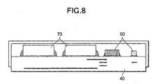
- the module according to the present embodiment has a height of 1.5 mm.
- the height is about 2 mm. It is apparent that the height is sufficiently reduced in comparison with the conventional one as shown in Fig. 8.
- the same members as or corresponding to the members of Fig. 1 are denoted with the same reference numerals.
- Fig. 4 shows the temperature characteristics when the flip chip of the SAW element is mounted on the ceramic multi-layer substrate as the present embodiment (dotted line), and when the flip chip is mounted likewise on the resin substrate (solid line) . It may be seen that the ceramic multi-layer substrate is less in change of frequency in company with the temperature change.
- Table 1 shows the shear strength when the test samples were produced by changing the cleaning process to non-cleaning, alkali chemical liquid cleaning and plasma cleaning respectively.
- the diameter of the gold bump was 100 ⁇ m after mounting the flip chip 30, the gap distance between the mounted electrode 43 and the flip chip 30 on the substrate 40 was 20 ⁇ m, and the gold plated film of the mounted electrode 43 of the substrate side was 0.5 ⁇ m.
- Table 1 Influences of the cleaning process to the shear strength. Cleaning ways Shear strength Non-cleaning 350 Chemical liquid cleaning 400 Plasma cleaning : 450W 1 min 360 2 min 420 3 min 450 5 min 460 8 min 460 10 min 360 15 min 320
- Table 2 shows the shear strength when the test samples were produced by changing the gold plated thickness of the mounted electrode 43 on the substrate 40 in the region 0.05 ⁇ m to 7.0 ⁇ m with respect to a 1005 chip inductor (1 ⁇ 0.5 ⁇ 0.5 mm) as the flip chip 30 and the soldering member 50.
- the diameter of the gold bump was 100 ⁇ m after mounting the flip chip 30, the gap distance was 20 ⁇ m between the mounted electrode 43 and the flip chip 30 on the substrate 40, and the gap distance was 20 ⁇ m between the mounted electrode 43 and the 1005 chip inductor, and the plasma cleaning was for 5 minutes.
- Table 2 Influences of the plated thickness to the shear strength of the SAW element and the solder mounting chip respectively.
- the gold plated thickness as the gold film is preferably 0.1 ⁇ m or more and 5 ⁇ m or less, and more preferably in the region between 0.3 ⁇ m and 3 ⁇ m.
- Table 3 shows the results measured as to the influence that the diameter of the gold bump gave to the shear strength and the heat impact test of the flip chip 30 regarding the samples which were made respectively by changing the diameters of the gold bump in the region between 30 ⁇ m to 200 ⁇ m when the flip chip 30 as the SAW element was face-down-bonded to the substrate 40.
- Table 3 Influence that the diameter of the gold bump gives to the shear strength and the heat impact test result of the SAW element.
- Diameter of gold bump ( ⁇ m) Shear strength of SAW (gf) Failure in the heat impact test (among 100 pieces) 30 290 12 50 400 1 70 450 0 100 460 0 120 460 0 150 470 1 200 470 8
- the heat impact test was made for more clearing the conditions.
- the test conditions included -40°C at the low temperature side and 85°C at the high temperature side which were held for 30 minutes at 100 cycles respectively.
- the estimation was made by measuring the insertion loss of the SAW element. The one which was initially about 2 dB and came to 5 dB or more was decided as failure. The estimation was decided by the number of failure of 100 samples.
- the other measuring conditions included the gold plated film being 0.5 ⁇ m of the mounted electrode 43 of the substrate side, the gap being 20 ⁇ m between the mounting electrode 43 and the flip chip 30 on the substrate 40, and the plasma cleaning was 5 minutes.
- the gold bump is 50 ⁇ m or more and 150 ⁇ m or less at the time of mounting, and more preferably in the range of 70 ⁇ m to 120 ⁇ m.
- Table 4 shows the measured results as to the influence that the gap distance between the mounted electrode 43 and the flip chip 30 on the substrate 40 gave to the shear strength and the heat impact test result of the flip chip 30 by use of the samples prepared to have the gap varied in the region 3 ⁇ m to 70 ⁇ m between the mounting electrode 43 and the flip chip 30.
- the gold film of the mounting electrode 43 of the substrate side was 0.5 ⁇ m
- the gold lump diameter was 100 ⁇ m
- the plasma cleaning was for 5 minutes
- Table 4 Influence that the gap gives to the shear strength and the heat impact test result of the SAW element.
- the gap distance is less than 5 ⁇ m, the strength is sufficient, but the failure comes out so often at the heat impact test. In case the gap distance exceeds 50 ⁇ m, there is no problem at the heat impact test, but the shear strength remarkably decreases. Therefore, it is preferable that the gap distance is 5 ⁇ m or more and 50 ⁇ m or less, and more preferably in the range 10 ⁇ m to 30 ⁇ m.
- the radio frequency electronic circuit parts including the flip chip 30 as the ceramic multi-layer substrate 40 and the SAW element directly mounted thereon by use of the resin side walls 60 and the resin cover 61, the SAW element may be sealed airtight, the influence of the solder member 50 when producing is eliminated, the production efficiency is heightened, the reliability for use is increased, the mounting efficiency at mounting maybe increased, and further the product may be reduced in height.
- the gold plated film of the mounted electrode 43 formed on the ceramic multi-layer substrate 40 is set to be 0.1 ⁇ m or more and 5 ⁇ m or less
- the distance between the flip chip 30 as the SAW element and the mounted electrode 43 is set to be 5 ⁇ m or more and 50 ⁇ m or less
- the diameter of gold bump for gold-to-gold bonding when bonding is set to be 50 ⁇ m or more and 50 ⁇ m or less.
- the manufacturing method at least the member bonding portion of the surface conductive layer 42 of the member mounting ceramic multi-layer substrate 40 is gold-plated to form the mounting electrode 43, the members except at least one SAW element are mounted by soldering, the cleaning is performed, subsequently the flip chip 30 as the SAW element is flip-chip mounted to the ceramic multi-layer substrate 40 by way of gold-to-gold bonding though the resin material of the side walls 60 and the resin cover 61 are bonded with the adhesive.
- the solder members to be mounted by soldering may follow the conventional way.
- the gold plated surface is sufficiently wet and enough fixed.
- the cleaning is performed to activate the gold surface so that no obstacle appears for mounting.
- the general medicine liquid cleaning activate the gold surface to an extent of allowing the SAW element to be mounted.
- the cleaning by way of the plasma etching is more preferred. In this case, it is required to take a condition of giving no damage to other mounting members.
- the resin such as the side walls 60 and the cover 61 is bonded in vacuum so that dirt around the SAW and the attached matters may be eliminated.
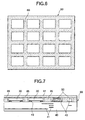
- Figs. 5A to 5E show a second embodiment, showing that a plurality of pieces of the ceramic multi-layer substrates are treated in a lump.
- the processes are the same as the processes shown in Fig. 2A to 2D, from mounting of the solder member on each ceramic multi-layer substrate 40 to cleaning of the substrate as shown in Fig. 5A.
- Fig. 6 with preparation of a lattice like resin member 63 having a plurality of portions (preferably 10 or more) formed in one body as so many resin side walls 60, a plurality of ceramic multi-layer substrates 40 (preferably 10 or more) are bonded on the lattice like resin member 63 as shown in Fig. 5B.
- a plurality of ceramic multi-layer substrates 40 are bonded on the lattice like resin member 63 as shown in Fig. 5B.
- the flip chip 30 as the SAW element is face-down-bonded to a plurality of ceramic multi-layer substrates 40, and then as shown in Fig. 5D, a resin plate 64 having a plurality of covers 61 formed in one body is bonded as a lumped process. Finally, as shown in Fig. 5E, the resin member 63 and the resin plate 64 are cut to be divided as individual members each having one ceramic multi-layer substrates 40.
- Figs. 5A to 5E the same portions as or corresponding to the portions of Figs . 2A to 2G are denoted by use of the same reference numerals.
- solder member 50 In the generally available mounting of the solder member 50, a metal mask is placed on the flat substrate 40, and the solder paste is print-coated, and the member 50 is arranged and the solder is fixed through the reflow furnace. Therefore, in case the resin member 63 as the side walls is bonded before the soldering process, the surface becomes uneven and the normal solder paste coating is difficult.
- a plurality of ceramic multi-layer substrates 40 may be treated in a lump at least in a certain part of the production processes base, thereby to considerably save labor, increase the production efficiency and accomplish the cost-down. Namely, (5) the problem for increasing the production efficiency by treating a plurality of ceramic multi-layer substrates board in a lump may be solved.
- Fig. 7 is a third embodiment, showing that the SAW element is isolated from the other members.
- the resin member 66 forming the side walls 65 is not simply square, but has holes hollowed out for receiving therein the flip chip 30 as the SAW element and the solder member 50 individually.
- the resin member 66 is bonded on the ceramic multi-layer substrates 40, and the epoxy resin plate as the cover 61 is bonded by the adhesive.
- the other part of structure is the same as the first embodiment.
- the same or corresponding members are denoted by the same reference numerals.
- the resin side walls 65 may be also provided between the flip chip 30 as the SAW element and the solder members as the other mounting members.
- each member may be isolated from the other members . Therefore, even if contaminating matter is produced from the other mounting members in practical use, this will not deteriorate the property of the SAW element.
- the structure of the resin side walls 65 and the cover 61 may be further preferably consolidated. The other working effects are the same as those of the first embodiment.
- the surface acoustic wave elements and other surface mounting elements are mounted on the ceramic multi-layer substrate, wherein the surface acoustic wave elements are flip chips which are face-down-bonded by way of gold-to-gold bonding to the gold coated electrodes of the ceramic multi-layer substrate, and at least the surface acoustic wave elements are covered as sealed airtight by the side walls fixed to the multi-layer ceramic substrate and the cover covering the opening of the side walls. Therefore, the SAW elements may be kept airtight and the influence of the soldered surface mounting elements at the time of production is eliminated. Further, the productivity, the reliability for use and the mounting efficiency at the time of mounting may be increased, and further the height of the product may be reduced.
Landscapes
- Physics & Mathematics (AREA)
- Acoustics & Sound (AREA)
- Surface Acoustic Wave Elements And Circuit Networks Thereof (AREA)
- Wire Bonding (AREA)
Abstract
Description
| Table 1 : Influences of the cleaning process to the shear strength. | |
| Cleaning ways | Shear strength |
| Non-cleaning | 350 |
| Chemical liquid cleaning | 400 |
| Plasma cleaning : | |
| 1 min | 360 |
| 2 min | 420 |
| 3 min | 450 |
| 5 min | 460 |
| 8 min | 460 |
| 10 min | 360 |
| 15 min | 320 |
| Table 2 : Influences of the plated thickness to the shear strength of the SAW element and the solder mounting chip respectively. | ||
| Gold plated thickness (µm) | Shear strength of SAW (gf) | Shear strength of chip parts (gf) |
| 0.05 | 310 | 800 |
| 0.1 | 400 | 1200 |
| 0.3 | 420 | 1500 |
| 0.5 | 460 | 1600 |
| 1.0 | 470 | 1700 |
| 2.0 | 480 | 1600 |
| 3.0 | 470 | 1700 |
| 5.0 | 480 | 1700 |
| 7.0 | 480 | 800 Peeling Occurred |
| Table 3: Influence that the diameter of the gold bump gives to the shear strength and the heat impact test result of the SAW element. | ||
| Diameter of gold bump (µm) | Shear strength of SAW (gf) | Failure in the heat impact test (among 100 pieces) |
| 30 | 290 | 12 |
| 50 | 400 | 1 |
| 70 | 450 | 0 |
| 100 | 460 | 0 |
| 120 | 460 | 0 |
| 150 | 470 | 1 |
| 200 | 470 | 8 |
| Table 4: Influence that the gap gives to the shear strength and the heat impact test result of the SAW element. | ||
| Gap distance (µm) | Shear strength of SAW (gf) | Failure in the heat impact test (among 100 pieces) |
| 3 | 450 | 15 |
| 5 | 440 | 2 |
| 10 | 450 | 0 |
| 20 | 460 | 0 |
| 30 | 460 | 0 |
| 50 | 410 | 0 |
| 70 | 340 | 0 |
Claims (8)
- A radio frequency module parts comprising:wherein at least said surface acoustic wave elements being covered airtight with side walls fixed to said ceramic multi-layer substrate and said cover covering the opening of said side walls.a ceramic multi-layer substrate;a surface acoustic wave element and other surface mounting elements mounted on said ceramic multi-layer substrate, said surface acoustic wave elements being flip chips which are face-down-bonded by way of gold-to-gold bonding to gold-coated electrodes of said ceramic multi-layer substrate; anda cover which seals the acoustic wave element,
- The radio frequency module parts including surface acoustic wave elements as set forth in claim 1, wherein at least one of said other surface mounting elements is mounted on the ceramic multi-layer substrate by way of soldering.
- The radio frequency module parts including surface acoustic wave elements as set forth in claim 1 or 2, wherein said surface acoustic wave elements are isolated from said other surface mounting elements by the side walls and the cover.
- The radio frequency module parts including surface elastic wave elements as set forth in claim 1 or 2, wherein the area of a portion surrounded by the side walls and covered by the cover is 30 % or more and 100 % or less of said ceramic multi-layer substrate.
- The radio frequency module parts including surface elastic wave elements as set forth in claim 1, or 2, wherein the gold film of the goldplated electrodes of the ceramic multi-layer substrate is between 0.1 µm or more and 5µm or less, the space between the surface acoustic wave elements and the gold plated electrodes is between 5µm or more and 50µm or less, and the diameter after bonding the goldbumps for the gold-to-gold bonding is between 50µm or more and 150 µm or less.
- A manufacturing method of radio frequency module parts including surface acoustic wave elements, characterized by comprising the steps of:plating a gold plate to at least portions of bonding parts of conductive surfaces of a ceramic multi-layer substrate;mounting by soldering, after said plating procedure, at least one surface mounting element other than the surface acoustic wave elements to said ceramic multi-layer substrate;cleaning the multi-layer ceramic substrate after said soldering;mounting, after said cleaning procedure, flip chips of the surface acoustic wave elements via face-down-bonding to the ceramic multi-layer substrate by way of gold-to-gold bonding;bonding members becoming side walls to the ceramic multi-layer substrate; andsealing by airtight a space surrounded by the members becoming the side walls and a member becoming a cover by attaching the member becoming the cover after mounting the surface acoustic wave elements and forming the side walls.
- The manufacturing method of the radio frequency module parts including the surface acoustic wave elements as set forth in claim 6, wherein said side wall forming procedure is carried out by bonding said side wall forming members in common to plural pieces of the ceramic multi-layer substrates, and at least parts of the following steps thereafter are carried out in a lump, and the members finally becoming the said sides are cut per each of ceramic multi-layer substrates.
- The manufacturing method of the radio frequency module parts including the surface acoustic wave elements as set forth in claim 6 or 7, wherein the cleaning procedure is for cleaning said ceramic multi-layer substrate by way of a plasma etching.
Applications Claiming Priority (2)
| Application Number | Priority Date | Filing Date | Title |
|---|---|---|---|
| JP2000260206 | 2000-08-30 | ||
| JP2000260206A JP4049239B2 (en) | 2000-08-30 | 2000-08-30 | Method for manufacturing high-frequency module component including surface acoustic wave element |
Publications (3)
| Publication Number | Publication Date |
|---|---|
| EP1184979A2 true EP1184979A2 (en) | 2002-03-06 |
| EP1184979A3 EP1184979A3 (en) | 2002-03-27 |
| EP1184979B1 EP1184979B1 (en) | 2007-12-05 |
Family
ID=18748249
Family Applications (1)
| Application Number | Title | Priority Date | Filing Date |
|---|---|---|---|
| EP01120578A Expired - Lifetime EP1184979B1 (en) | 2000-08-30 | 2001-08-29 | Radio frequency module parts including surface elastic wave elements and manufacturing method thereof |
Country Status (6)
| Country | Link |
|---|---|
| US (1) | US6628178B2 (en) |
| EP (1) | EP1184979B1 (en) |
| JP (1) | JP4049239B2 (en) |
| CN (1) | CN1214458C (en) |
| DE (1) | DE60131712T2 (en) |
| MY (1) | MY128586A (en) |
Cited By (8)
| Publication number | Priority date | Publication date | Assignee | Title |
|---|---|---|---|---|
| WO2003067649A1 (en) * | 2002-02-05 | 2003-08-14 | Toray Engineering Co., Ltd. | Chip mounting method and device using it |
| FR2838577A1 (en) * | 2002-04-12 | 2003-10-17 | Thales Sa | MODULE COMPRISING INTERFACE ACOUSTIC WAVE COMPONENTS |
| EP1187320A3 (en) * | 2000-09-07 | 2004-09-22 | TDK Corporation | Method for manufacturing radio frequency module components with surface acoustic wave element |
| WO2004051745A3 (en) * | 2002-12-05 | 2005-02-24 | Epcos Ag | Electronic component comprising a plurality of chips and method for producing the same |
| WO2005101502A1 (en) * | 2004-04-16 | 2005-10-27 | Koninklijke Philips Electronics N.V. | An integrated circuit, a method and an assembly for manufacturing the integrated circuit, and a mobile phone having the integrated circuit |
| US7567148B2 (en) | 2004-11-04 | 2009-07-28 | Epcos Ag | Frequency shunt |
| EP1445861A3 (en) * | 2003-01-07 | 2009-10-28 | Hitachi Ltd. | Electronic device and method of manufacturing the same |
| EP2757686A1 (en) * | 2013-01-18 | 2014-07-23 | Murata Manufacturing Co., Ltd. | Filter circuit |
Families Citing this family (37)
| Publication number | Priority date | Publication date | Assignee | Title |
|---|---|---|---|---|
| JP2002118486A (en) * | 2000-10-06 | 2002-04-19 | Matsushita Electric Ind Co Ltd | High frequency composite switch module |
| EP1333588B1 (en) * | 2000-11-01 | 2012-02-01 | Hitachi Metals, Ltd. | High-frequency switch module |
| US6865376B2 (en) * | 2001-07-03 | 2005-03-08 | Kyocera Wireless Corp. | System and method for a GPS enabled antenna |
| JP4020644B2 (en) * | 2002-01-09 | 2007-12-12 | アルプス電気株式会社 | SAW filter module |
| DE10228328A1 (en) * | 2002-06-25 | 2004-01-22 | Epcos Ag | Electronic component with a multilayer substrate and manufacturing process |
| JP2004201285A (en) * | 2002-12-06 | 2004-07-15 | Murata Mfg Co Ltd | Method of manufacturing piezoelectric component and piezoelectric component |
| JP2004194240A (en) * | 2002-12-13 | 2004-07-08 | Murata Mfg Co Ltd | Three demultiplexer/multiplexer |
| JP3938147B2 (en) * | 2003-04-08 | 2007-06-27 | 住友金属鉱山株式会社 | Lithium tantalate substrate and manufacturing method thereof |
| US7376440B2 (en) * | 2003-04-16 | 2008-05-20 | Kyocera Wireless Corp. | N-plexer systems and methods for use in a wireless communications device |
| US6980067B2 (en) * | 2003-04-16 | 2005-12-27 | Kyocera Wireless Corp. | Triplexer systems and methods for use in wireless communications device |
| TW200520201A (en) | 2003-10-08 | 2005-06-16 | Kyocera Corp | High-frequency module and communication apparatus |
| JP2005136683A (en) * | 2003-10-30 | 2005-05-26 | Tdk Corp | Electronic components |
| JP2005159157A (en) * | 2003-11-27 | 2005-06-16 | Renesas Technology Corp | Semiconductor device |
| US20050227417A1 (en) * | 2004-04-06 | 2005-10-13 | Honeywell International Inc. | Packaging assembly utilizing flip chip and conductive plastic traces |
| TWI250629B (en) * | 2005-01-12 | 2006-03-01 | Ind Tech Res Inst | Electronic package and fabricating method thereof |
| US8467827B2 (en) * | 2005-03-31 | 2013-06-18 | Black Sand Technologies, Inc. | Techniques for partitioning radios in wireless communication systems |
| US20070051176A1 (en) * | 2005-09-08 | 2007-03-08 | Honeywell International Inc. | Passive hybrid lc/SAW/BAW wireless sensor |
| KR101206030B1 (en) * | 2006-01-25 | 2012-11-28 | 삼성전자주식회사 | RF module, multi RF module, and method of fabricating thereof |
| JP4863746B2 (en) * | 2006-03-27 | 2012-01-25 | 富士通株式会社 | Semiconductor device and manufacturing method thereof |
| JP4555369B2 (en) | 2008-08-13 | 2010-09-29 | 富士通メディアデバイス株式会社 | Electronic component module and manufacturing method thereof |
| US8554136B2 (en) | 2008-12-23 | 2013-10-08 | Waveconnex, Inc. | Tightly-coupled near-field communication-link connector-replacement chips |
| US9322904B2 (en) | 2011-06-15 | 2016-04-26 | Keyssa, Inc. | Proximity sensing using EHF signals |
| US9407311B2 (en) | 2011-10-21 | 2016-08-02 | Keyssa, Inc. | Contactless signal splicing using an extremely high frequency (EHF) communication link |
| JP5556072B2 (en) * | 2009-01-07 | 2014-07-23 | ソニー株式会社 | Semiconductor device, method of manufacturing the same, and millimeter wave dielectric transmission device |
| CN102118140A (en) * | 2010-01-04 | 2011-07-06 | 姚一滨 | Multi-variant united-row composite substrate, frequency device group and manufacturing method thereof |
| US20110168784A1 (en) * | 2010-01-14 | 2011-07-14 | Rfmarq, Inc. | Wireless Communication Device for Remote Authenticity Verification of Semiconductor Chips, Multi-Chip Modules and Derivative Products |
| TWI595715B (en) | 2012-08-10 | 2017-08-11 | 奇沙公司 | Dielectric coupling system for extremely high frequency communication |
| CN104769852B (en) | 2012-09-14 | 2016-09-21 | 凯萨股份有限公司 | Wireless connection with virtual hysteresis |
| CN104937769B (en) | 2012-12-17 | 2018-11-16 | 凯萨股份有限公司 | Modular Electronics |
| EP2974504B1 (en) | 2013-03-15 | 2018-06-20 | Keyssa, Inc. | Ehf secure communication device |
| WO2014145366A2 (en) | 2013-03-15 | 2014-09-18 | Keyssa, Inc. | Extremely high frequency communication chip |
| US9093563B2 (en) * | 2013-07-11 | 2015-07-28 | International Business Machines Corporation | Electronic module assembly with patterned adhesive array |
| JP6360678B2 (en) * | 2013-12-09 | 2018-07-18 | 太陽誘電株式会社 | Module and manufacturing method thereof |
| KR102428141B1 (en) * | 2014-02-25 | 2022-08-02 | 스카이워크스 솔루션즈, 인코포레이티드 | Systems, devices and methods related to improved radio-frequency modules |
| US10944379B2 (en) * | 2016-12-14 | 2021-03-09 | Qualcomm Incorporated | Hybrid passive-on-glass (POG) acoustic filter |
| US11424195B2 (en) * | 2018-04-02 | 2022-08-23 | Intel Corporation | Microelectronic assemblies having front end under embedded radio frequency die |
| US11619128B2 (en) * | 2018-09-01 | 2023-04-04 | Baker Hughes Holdings Llc | Electronics assemblies for downhole use |
Family Cites Families (17)
| Publication number | Priority date | Publication date | Assignee | Title |
|---|---|---|---|---|
| JPS62173813A (en) * | 1986-01-28 | 1987-07-30 | Alps Electric Co Ltd | Surface acoustic wave element |
| JPS62173814A (en) * | 1986-01-28 | 1987-07-30 | Alps Electric Co Ltd | Mounting unit for surface acoustic wave element |
| JPH04170811A (en) * | 1990-11-05 | 1992-06-18 | Fujitsu Ltd | Surface acoustic wave device |
| JP3161831B2 (en) | 1992-09-09 | 2001-04-25 | 株式会社日立製作所 | Circuit element module |
| US5459368A (en) * | 1993-08-06 | 1995-10-17 | Matsushita Electric Industrial Co., Ltd. | Surface acoustic wave device mounted module |
| JP3194553B2 (en) * | 1993-08-13 | 2001-07-30 | 富士通株式会社 | Method for manufacturing semiconductor device |
| JP3301262B2 (en) * | 1995-03-28 | 2002-07-15 | 松下電器産業株式会社 | Surface acoustic wave device |
| JPH08288787A (en) * | 1995-04-10 | 1996-11-01 | Canon Inc | Surface acoustic wave device, spread spectrum communication device, and system using the same |
| JPH09148373A (en) * | 1995-11-21 | 1997-06-06 | Murata Mfg Co Ltd | Wireless communication module |
| DE69718693T2 (en) | 1996-03-08 | 2003-11-27 | Matsushita Electric Industrial Co., Ltd. | Electronic component and manufacturing process |
| JPH1079638A (en) | 1996-09-05 | 1998-03-24 | Oki Electric Ind Co Ltd | Surface acoustic wave filter and its production |
| US5872493A (en) * | 1997-03-13 | 1999-02-16 | Nokia Mobile Phones, Ltd. | Bulk acoustic wave (BAW) filter having a top portion that includes a protective acoustic mirror |
| JP3982876B2 (en) * | 1997-06-30 | 2007-09-26 | 沖電気工業株式会社 | Surface acoustic wave device |
| JP3579740B2 (en) * | 1998-04-18 | 2004-10-20 | Tdk株式会社 | Manufacturing method of electronic components |
| JP3109477B2 (en) * | 1998-05-26 | 2000-11-13 | 日本電気株式会社 | Multi-chip module |
| JP3303791B2 (en) * | 1998-09-02 | 2002-07-22 | 株式会社村田製作所 | Electronic component manufacturing method |
| SG108217A1 (en) * | 1998-12-29 | 2005-01-28 | Toshiba Kk | Surface acoustic wave device |
-
2000
- 2000-08-30 JP JP2000260206A patent/JP4049239B2/en not_active Expired - Fee Related
-
2001
- 2001-08-27 MY MYPI20014013A patent/MY128586A/en unknown
- 2001-08-29 US US09/940,440 patent/US6628178B2/en not_active Expired - Lifetime
- 2001-08-29 EP EP01120578A patent/EP1184979B1/en not_active Expired - Lifetime
- 2001-08-29 DE DE60131712T patent/DE60131712T2/en not_active Expired - Lifetime
- 2001-08-30 CN CNB011357436A patent/CN1214458C/en not_active Expired - Fee Related
Cited By (13)
| Publication number | Priority date | Publication date | Assignee | Title |
|---|---|---|---|---|
| EP1187320A3 (en) * | 2000-09-07 | 2004-09-22 | TDK Corporation | Method for manufacturing radio frequency module components with surface acoustic wave element |
| WO2003067649A1 (en) * | 2002-02-05 | 2003-08-14 | Toray Engineering Co., Ltd. | Chip mounting method and device using it |
| FR2838577A1 (en) * | 2002-04-12 | 2003-10-17 | Thales Sa | MODULE COMPRISING INTERFACE ACOUSTIC WAVE COMPONENTS |
| WO2003088482A1 (en) * | 2002-04-12 | 2003-10-23 | Thales | Module comprising acoustic wave interface components |
| WO2004051745A3 (en) * | 2002-12-05 | 2005-02-24 | Epcos Ag | Electronic component comprising a plurality of chips and method for producing the same |
| EP1445861A3 (en) * | 2003-01-07 | 2009-10-28 | Hitachi Ltd. | Electronic device and method of manufacturing the same |
| US7961478B2 (en) | 2004-04-16 | 2011-06-14 | Nxp B.V. | Integrated circuit, and a mobile phone having the integrated circuit |
| WO2005101502A1 (en) * | 2004-04-16 | 2005-10-27 | Koninklijke Philips Electronics N.V. | An integrated circuit, a method and an assembly for manufacturing the integrated circuit, and a mobile phone having the integrated circuit |
| US7567148B2 (en) | 2004-11-04 | 2009-07-28 | Epcos Ag | Frequency shunt |
| EP2757686A1 (en) * | 2013-01-18 | 2014-07-23 | Murata Manufacturing Co., Ltd. | Filter circuit |
| CN103944526A (en) * | 2013-01-18 | 2014-07-23 | 株式会社村田制作所 | Filter circuit |
| US9331658B2 (en) | 2013-01-18 | 2016-05-03 | Murata Manufacturing Co., Ltd. | Filter circuit |
| CN103944526B (en) * | 2013-01-18 | 2017-04-12 | 株式会社村田制作所 | Filter circuit |
Also Published As
| Publication number | Publication date |
|---|---|
| CN1340856A (en) | 2002-03-20 |
| MY128586A (en) | 2007-02-28 |
| DE60131712T2 (en) | 2008-04-10 |
| JP2002076832A (en) | 2002-03-15 |
| EP1184979A3 (en) | 2002-03-27 |
| CN1214458C (en) | 2005-08-10 |
| US20020044030A1 (en) | 2002-04-18 |
| DE60131712D1 (en) | 2008-01-17 |
| EP1184979B1 (en) | 2007-12-05 |
| JP4049239B2 (en) | 2008-02-20 |
| US6628178B2 (en) | 2003-09-30 |
Similar Documents
| Publication | Publication Date | Title |
|---|---|---|
| EP1184979B1 (en) | Radio frequency module parts including surface elastic wave elements and manufacturing method thereof | |
| EP1191829B1 (en) | Surface electrode structure on ceramic multi-layer substrate and process for producing the same | |
| US6698084B2 (en) | Method for manufacturing radio frequency module components with surface acoustic wave element | |
| US8043896B2 (en) | Semiconductor chip, method of manufacturing the semiconductor chip and semiconductor chip package including an inclined via hole | |
| CN1638272B (en) | Surface acoustic wave device,electronic circuit device, communication device and electronic device | |
| US7816794B2 (en) | Electronic device and method of fabricating the same | |
| US20050116352A1 (en) | Acoustic wave device and method of fabricating the same | |
| US20030159262A1 (en) | High frequency device packages and methods | |
| US20040159960A1 (en) | Electronic device and method of manufacturing the same | |
| US7315455B2 (en) | Surface-mounted electronic component module and method for manufacturing the same | |
| US20110038132A1 (en) | Microstructure Apparatus, Manufacturing Method Thereof, and Sealing Substrate | |
| WO2009001170A2 (en) | Filter having impedance matching circuits | |
| EP1020908B1 (en) | Resin-sealed surface mounting type electronic parts | |
| US6627966B2 (en) | Method and device for sealing ceramic package of saw filter | |
| JP4582352B2 (en) | High frequency module component including surface acoustic wave device and assembly thereof | |
| JP2002261581A (en) | High frequency module components | |
| JP2003008393A (en) | High frequency module components | |
| WO2025197559A1 (en) | High-frequency module and communication device | |
| HK1029868A (en) | Resin-sealed surface mounting type electronic parts |
Legal Events
| Date | Code | Title | Description |
|---|---|---|---|
| PUAI | Public reference made under article 153(3) epc to a published international application that has entered the european phase |
Free format text: ORIGINAL CODE: 0009012 |
|
| PUAL | Search report despatched |
Free format text: ORIGINAL CODE: 0009013 |
|
| AK | Designated contracting states |
Kind code of ref document: A2 Designated state(s): AT BE CH CY DE DK ES FI FR GB GR IE IT LI LU MC NL PT SE TR Kind code of ref document: A2 Designated state(s): DE FR GB |
|
| AX | Request for extension of the european patent |
Free format text: AL;LT;LV;MK;RO;SI |
|
| AK | Designated contracting states |
Kind code of ref document: A3 Designated state(s): AT BE CH CY DE DK ES FI FR GB GR IE IT LI LU MC NL PT SE TR |
|
| AX | Request for extension of the european patent |
Free format text: AL;LT;LV;MK;RO;SI |
|
| 17P | Request for examination filed |
Effective date: 20020529 |
|
| AKX | Designation fees paid |
Free format text: DE FR GB |
|
| 17Q | First examination report despatched |
Effective date: 20070122 |
|
| GRAP | Despatch of communication of intention to grant a patent |
Free format text: ORIGINAL CODE: EPIDOSNIGR1 |
|
| GRAS | Grant fee paid |
Free format text: ORIGINAL CODE: EPIDOSNIGR3 |
|
| GRAA | (expected) grant |
Free format text: ORIGINAL CODE: 0009210 |
|
| AK | Designated contracting states |
Kind code of ref document: B1 Designated state(s): DE FR GB |
|
| REG | Reference to a national code |
Ref country code: GB Ref legal event code: FG4D |
|
| REF | Corresponds to: |
Ref document number: 60131712 Country of ref document: DE Date of ref document: 20080117 Kind code of ref document: P |
|
| ET | Fr: translation filed | ||
| PLBE | No opposition filed within time limit |
Free format text: ORIGINAL CODE: 0009261 |
|
| STAA | Information on the status of an ep patent application or granted ep patent |
Free format text: STATUS: NO OPPOSITION FILED WITHIN TIME LIMIT |
|
| 26N | No opposition filed |
Effective date: 20080908 |
|
| REG | Reference to a national code |
Ref country code: GB Ref legal event code: 746 Effective date: 20091211 |
|
| PGFP | Annual fee paid to national office [announced via postgrant information from national office to epo] |
Ref country code: FR Payment date: 20110818 Year of fee payment: 11 Ref country code: GB Payment date: 20110824 Year of fee payment: 11 |
|
| GBPC | Gb: european patent ceased through non-payment of renewal fee |
Effective date: 20120829 |
|
| REG | Reference to a national code |
Ref country code: FR Ref legal event code: ST Effective date: 20130430 |
|
| PG25 | Lapsed in a contracting state [announced via postgrant information from national office to epo] |
Ref country code: GB Free format text: LAPSE BECAUSE OF NON-PAYMENT OF DUE FEES Effective date: 20120829 |
|
| PG25 | Lapsed in a contracting state [announced via postgrant information from national office to epo] |
Ref country code: FR Free format text: LAPSE BECAUSE OF NON-PAYMENT OF DUE FEES Effective date: 20120831 |
|
| REG | Reference to a national code |
Ref country code: DE Ref legal event code: R082 Ref document number: 60131712 Country of ref document: DE Representative=s name: BARDEHLE PAGENBERG PARTNERSCHAFT MBB PATENTANW, DE Ref country code: DE Ref legal event code: R081 Ref document number: 60131712 Country of ref document: DE Owner name: SNAPTRACK, INC., SAN DIEGO, US Free format text: FORMER OWNER: TDK CORP., TOKYO, JP |
|
| REG | Reference to a national code |
Ref country code: DE Ref legal event code: R081 Ref document number: 60131712 Country of ref document: DE Owner name: SNAPTRACK, INC., SAN DIEGO, US Free format text: FORMER OWNER: SNAPTRACK INC., SAN DIEGO, CALIF., US Ref country code: DE Ref legal event code: R082 Ref document number: 60131712 Country of ref document: DE Representative=s name: BARDEHLE PAGENBERG PARTNERSCHAFT MBB PATENTANW, DE |
|
| PGFP | Annual fee paid to national office [announced via postgrant information from national office to epo] |
Ref country code: DE Payment date: 20170825 Year of fee payment: 17 |
|
| REG | Reference to a national code |
Ref country code: DE Ref legal event code: R119 Ref document number: 60131712 Country of ref document: DE |
|
| PG25 | Lapsed in a contracting state [announced via postgrant information from national office to epo] |
Ref country code: DE Free format text: LAPSE BECAUSE OF NON-PAYMENT OF DUE FEES Effective date: 20190301 |