EP1184977A2 - Multilayered LC composite component and method for adjusting frequency of the same - Google Patents
Multilayered LC composite component and method for adjusting frequency of the same Download PDFInfo
- Publication number
- EP1184977A2 EP1184977A2 EP01116118A EP01116118A EP1184977A2 EP 1184977 A2 EP1184977 A2 EP 1184977A2 EP 01116118 A EP01116118 A EP 01116118A EP 01116118 A EP01116118 A EP 01116118A EP 1184977 A2 EP1184977 A2 EP 1184977A2
- Authority
- EP
- European Patent Office
- Prior art keywords
- electrode
- trimming
- multilayered
- electrodes
- composite component
- Prior art date
- Legal status (The legal status is an assumption and is not a legal conclusion. Google has not performed a legal analysis and makes no representation as to the accuracy of the status listed.)
- Granted
Links
Images


Classifications
-
- H—ELECTRICITY
- H03—ELECTRONIC CIRCUITRY
- H03H—IMPEDANCE NETWORKS, e.g. RESONANT CIRCUITS; RESONATORS
- H03H7/00—Multiple-port networks comprising only passive electrical elements as network components
- H03H7/01—Frequency selective two-port networks
- H03H7/09—Filters comprising mutual inductance
-
- H—ELECTRICITY
- H03—ELECTRONIC CIRCUITRY
- H03H—IMPEDANCE NETWORKS, e.g. RESONANT CIRCUITS; RESONATORS
- H03H7/00—Multiple-port networks comprising only passive electrical elements as network components
- H03H7/01—Frequency selective two-port networks
- H03H7/17—Structural details of sub-circuits of frequency selective networks
- H03H7/1708—Comprising bridging elements, i.e. elements in a series path without own reference to ground and spanning branching nodes of another series path
-
- H—ELECTRICITY
- H03—ELECTRONIC CIRCUITRY
- H03H—IMPEDANCE NETWORKS, e.g. RESONANT CIRCUITS; RESONATORS
- H03H7/00—Multiple-port networks comprising only passive electrical elements as network components
- H03H7/01—Frequency selective two-port networks
- H03H7/17—Structural details of sub-circuits of frequency selective networks
- H03H7/1741—Comprising typical LC combinations, irrespective of presence and location of additional resistors
- H03H7/1775—Parallel LC in shunt or branch path
-
- H—ELECTRICITY
- H03—ELECTRONIC CIRCUITRY
- H03H—IMPEDANCE NETWORKS, e.g. RESONANT CIRCUITS; RESONATORS
- H03H1/00—Constructional details of impedance networks whose electrical mode of operation is not specified or applicable to more than one type of network
- H03H2001/0021—Constructional details
- H03H2001/0078—Constructional details comprising spiral inductor on a substrate
-
- H—ELECTRICITY
- H03—ELECTRONIC CIRCUITRY
- H03H—IMPEDANCE NETWORKS, e.g. RESONANT CIRCUITS; RESONATORS
- H03H1/00—Constructional details of impedance networks whose electrical mode of operation is not specified or applicable to more than one type of network
- H03H2001/0021—Constructional details
- H03H2001/0085—Multilayer, e.g. LTCC, HTCC, green sheets
-
- H—ELECTRICITY
- H03—ELECTRONIC CIRCUITRY
- H03H—IMPEDANCE NETWORKS, e.g. RESONANT CIRCUITS; RESONATORS
- H03H2210/00—Indexing scheme relating to details of tunable filters
- H03H2210/01—Tuned parameter of filter characteristics
- H03H2210/012—Centre frequency; Cut-off frequency
Definitions
- the present invention relates to multilayered LC composite components such as multilayered LC filters and methods for adjusting the frequencies of the composite components.
- the multilayered LC filter is a chip-shaped LC composite component formed by laminating internal electrodes including capacitor electrodes and inductor electrodes with dielectric layers. Such a multilayered LC filter is suitable for miniaturization.
- a trimming electrode opposing internal electrodes is first arranged on a surface of the multilayered LC filter, and next, a portion of the trimming electrode is removed via laser, or by sandblasting or some other cutting method, which is referred to as a so-called functional trimming method.
- preferred embodiments of the present invention provide a multilayered LC composite component in which fine adjustments to a desired frequency can be easily and accurately made. Additionally, preferred embodiments of the present invention provide a method for adjusting the frequency of the composite component.
- a multilayered LC composite component includes a multilayered body having internal electrodes including capacitor electrodes and an inductor electrode which are laminated via dielectric layers, input/output external electrodes and a ground external electrode disposed on a surface of the multilayered body, a trimming electrode disposed on a surface of the multilayered body such that the trimming electrode is opposed to at least one of the internal electrodes and electrically connected to the ground external electrode, an isolated electrode that is separated from the trimming electrode by a trimming groove, and a coating material filled in the trimming groove, the coating material having a dielectric constant that is smaller than the dielectric constant of the dielectric layer.
- the frequency of the multilayered LC composite component can be adjusted to a desired frequency by forming a capacitance between the internal electrodes and the trimming electrode, between the internal electrodes and the isolated electrode, and between the trimming electrode and the isolated electrode.
- a rough adjustment is made by forming the isolated electrode, which is separated from the trimming electrode, and next, a fine adjustment is made by filling the coating material in the trimming groove, with the result that the frequency of the multilayered LC composite component can be adjusted to the desired frequency.
- the isolated electrode may be an insular electrode surrounded by the trimming electrode via the trimming groove.
- the coating material may have a dielectric constant between about 1.5 and about 10.
- the dielectric constant of the coating material since the fine adjustment is performed by applying the coating material, it is preferable that the dielectric constant of the coating material is small.
- the dielectric constant is extremely small, the maximum of the varying range is limited.
- the minimum dielectric constant is about 1.5 or greater.
- the maximum dielectric constant is about 10 or smaller.
- a method for adjusting the frequency of a multilayered LC composite component including a multilayered body in which internal electrodes having capacitor electrodes and an inductor electrode are laminated via dielectric layers, input/output external electrodes and a ground external electrode disposed on surfaces of the multilayered body, and a trimming electrode disposed on a surface of the multilayered body such that the trimming electrode is opposed to at least one of the internal electrodes and electrically connected to the ground external electrode, the method including the steps of making a primary adjustment in which trimming groove is formed in the trimming electrode to form the isolated electrode separated from the trimming electrode so that a capacitance between the trimming electrode and the internal electrode is reduced to be smaller than a capacitance for a desired frequency, and making a secondary adjustment in which a coating material having a dielectric constant that is smaller than the dielectric constant of the dielectric layer is filled in the trimming groove to slightly increase a capacitance between the trimming electrode and the isolated electrode so as to adjust to the desired frequency.
- the adjustment for obtaining the desired frequency is performed preferably via two steps including the primary adjustment as the rough adjustment and the secondary adjustment as the fine adjustment. That is, first, before the formation of the electrode isolated from the trimming electrode, the one capacitance is present between the trimming electrode and the internal electrode. Then, after the formation of the isolated electrode, two capacitances are generated, that is, the capacitance between the trimming electrode and the internal electrode and the capacitance between the internal electrode and the isolated electrode. This is the primary step for the adjustment forming the two capacitances.
- the isolated electrode separated by the trimming groove is a floating electrode that is disconnected from the ground external electrode, a potential difference between the isolated electrode and the internal electrode is smaller than a potential difference between the internal electrode and the trimming electrode connected to the ground external electrode.
- a synthesized capacitance obtained after the isolation is smaller than the capacitance obtained before the isolation.
- the synthesized capacitance between the trimming electrode and the internal electrodes is temporarily smaller than the synthesized capacitance in which the desired frequency is obtainable.
- the secondary adjustment is performed by filling the coating material in at least the trimming groove.
- the coating material is applied on the multilayered body to generate a small amount of capacitance between the trimming electrode and the isolated electrode mutually opposing in a surface direction via the coating material.
- the capacitance between the trimming electrode and the isolated electrode slightly increases, a synthesized capacitance obtained from the three capacitances also slightly increases.
- the temporarily reduced synthesized capacitance in the primary adjustment can be slightly increased in the secondary adjustment. Consequently, the synthesized capacitance can be closer to the capacitance for the desired frequency.
- Fig. 1 shows an exploded perspective view illustrating the multilayered LC filter of the present preferred embodiment of the present invention.
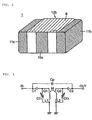
- Fig. 2 shows a perspective view for illustrating the appearance of the multilayered LC filter shown in Fig. 1.
- Fig. 3 shows an equivalent circuit diagram of the multilayered LC filter.
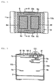
- Fig. 4 shows a schematic plan view of the multilayered LC filter.
- Fig. 5 shows a sectional view of the multilayered LC filter along the line A-A' shown in Fig. 4.
- a multilayered LC filter 1 includes a dielectric sheet 2a having a ground internal electrode 3 disposed thereon, a dielectric sheet 2b having a pair of inductor electrodes 4a and 4b disposed thereon, a dielectric sheet 2c having a coupling capacitor electrode 5 disposed thereon, a dielectric sheet 2d having an input extraction electrode 6a and an output extraction electrode 6b disposed thereon, a dielectric sheet 2e having resonance capacitor electrodes 7a and 7b disposed thereon, and a dielectric sheet 2f having a trimming electrode 8 disposed thereon.
- Each of the internal electrodes and the trimming electrode 8 is preferably made of Ag, Pd, Cu, Ni, Au, Ag-Pd, or other suitable material, and is formed by printing, sputtering, vapor deposition, or other suitable method.
- the dielectric sheets 2a to 2f are preferably sheet members formed by mixing dielectric powder with a binder.
- the ground internal electrode 3 is disposed on the substantially entire top surface of the dielectric sheet 2a. One end 3a of the ground internal electrode 3 is exposed to the front edge of the dielectric sheet 2a, and the other end 3b is exposed to the back edge of the dielectric sheet 2a. On the outer peripheral region of the dielectric sheet 2a, there are disposed portions 3c where the ground internal electrode 3 is not formed to increase coupling strengths between the dielectric layers. When there is no concern about detachment, the ground internal electrode 3 may be disposed on the entire top surface of the dielectric sheet 2a.
- Each of the inductor electrodes 4a and 4b is defined preferably by a coil of substantially one turn.
- the inductor electrode 4a is located closer to the left of the dielectric sheet 2b, and the inductor electrode 4b is located closer to the right of the dielectric sheet 2b.
- One end 4a 1 of the inductor electrode 4a is connected to the resonance capacitor 7a by via-holes, and the other end 4a 2 thereof is connected to the ground internal electrode 3 by another via-hole.
- one end 4b 1 of the inductor electrode 4b is connected to the resonance capacitor 7b by via-holes, and the other end 4b 2 thereof is connected to the ground internal electrode 3 by another via-hole.
- the coupling capacitor electrode 5 has a substantially rectangular shape having longer edge lines extending in the left-and-right direction of the dielectric sheet 2c.
- the coupling capacitor electrode 5 is disposed on the front of the substantially center of the dielectric sheet 2c.
- One end 6a 1 of the input extraction electrode 6a is exposed to the left edge line of the dielectric sheet 2d, and the other end 6a 2 thereof has a large area opposing the coupling capacitor electrode 5 via the electric sheet 2d and also opposing the resonance capacitor electrode 7a via the dielectric sheet 2e.
- one end 6b 1 of the output extraction electrode 6b is exposed to the right edge line of the dielectric sheet 2d, and the other end 6b 2 thereof has a large area opposing the coupling capacitor electrode 5 via the electric sheet 2d and also opposing the resonance capacitor electrode 7b via the dielectric sheet 2e.
- Each of the resonance capacitor electrodes 7a and 7b has a substantially rectangular shape having longer edge lines are extended in the front-and-back direction of the electric sheet 2e.
- the resonance capacitor electrode 7a is located closer to the left of the dielectric sheet 2e, and the resonance capacitor electrode 7b is located closer to the right of the dielectric sheet 2e.
- the resonance capacitor electrode 7a is connected to the one end 4a 1 of the inductor electrode 4a, and is opposed to the input extraction electrode 6a.
- the resonance capacitor electrode 7a is also opposed to the trimming electrode 8 via the dielectric sheet 2f.
- the resonance capacitor electrode 7b is connected to the one end 4b 1 of the inductor electrode 4b and is opposed to the input extraction electrode 6b.
- the resonance capacitor electrode 7b is also opposed to the trimming electrode 8 via the dielectric sheet 2f.
- the trimming electrode 8 is disposed on the substantially entire top surface of the dielectric sheet 2f in a manner that the electrode 8 covers at least the resonance capacitor electrodes 7a and 7b.
- One end 8a of the trimming electrode 8 is exposed to the front edge line of the dielectric sheet 2f, and the other end 8b thereof is exposed to the back edge line of the dielectric sheet 2f.
- Each of the trimming grooves 8c and 8d preferably has a substantially rectangular shape in the region of the trimming electrode 8.
- insular electrodes 8e and 8f having substantially the same shape define isolated electrodes, which are isolated from the trimming electrode 8.
- the insular electrodes 8e and 8f are floating electrodes electrically disconnected from the ground external electrodes 10a and 10b.
- the electrodes 8e and 8f are substantially opposed to the resonance capacitor electrodes 7a and 7b via the dielectric sheet 2f.
- the shapes of the trimming grooves 8c and 8d and the shapes of the insular electrodes 8e and 8f are preferably formed after the dielectric sheets are laminated to define a multi-layered body which will be described below. Additionally, the shape of each of the insular electrodes 8e and 8f is not limited to the above-described shape. Any shape, such as a substantially round or substantially triangular shape, can be used in the present invention, as long as the shape can define a region that is enclosed with each of the trimming grooves 8c and 8d.
- the ground external electrodes 10a and 10b are disposed on the front and back side-surfaces of the obtained multilayered body.
- an input external electrode 11a and an output external electrode 11b are provided on the right and left side-surfaces of the multilayered body.
- These external electrodes are formed preferably by application/burning, sputtering, vapor deposition, or other suitable method.
- the ground external electrode 10a is connected to the one end 3a of the ground internal electrode 3 and the one end 8a of the trimming electrode 8.
- the ground external electrode 10b is connected to the other end 3b of the ground internal electrode 3 and the other end 8b of the trimming electrode 8. Additionally, the input external electrode 11a is connected to the one end 6a 1 of the input extraction electrode 6a, and the output external electrode 11b is connected to the one end 6b 1 of the output extraction electrode 6b.
- a coating material 9 is applied on the substantially entire surfaces of the multilayered body.
- the coating material 9 is moisture-resistant and has a dielectric constant between approximately 1.5 and approximately 10. That is, the dielectric constant of the coating material 9 to be used is preferably smaller than the dielectric constant of the dielectric (for example, a dielectric constant between about 6 and about 50) of the multilayered body.
- a composition for the coating material 9 having such a dielectric constant for example, there is included acrylic resin (a dielectric constant between about 2.5 and about 4), epoxy resin (a dielectric constant between about 3 and about 6), silicone resin (a dielectric constant between about 3.5 and about 6.5), or other suitable material, as the main component, and according to the needs, an additive such as a hardening agent and an accelerator may be mixed therewith.
- the dielectric constant may be adjusted by mixing an inorganic material such as a dielectric material as an additive to the coating material when needed. With such an additive mixed therewith, a dielectric constant smaller or greater than the dielectric constant of resin can be obtained. Thus, it is possible to easily obtain the dielectric constant between about 1.5 and about 10.
- the multilayered LC filter described above defines the equivalent circuit of a band pass filter as shown in Fig. 3. Specifically, an inductance L 1 of the inductor electrode 4a and a trimming capacitance Ct 1 , defined between the resonance capacitor electrode 7a and the trimming electrode 8 are connected in parallel between an input terminal and a ground terminal to constitute an LC parallel resonance circuit Q 1 on the input side.
- an inductance L 2 of the inductor electrode 4b and a trimming capacitance Ct 2 , defined between the resonance capacitor electrode 7b and the trimming electrode 8 are connected in parallel between an output terminal and a ground terminal to constitute an LC parallel resonance circuit Q 2 on the input side.
- a mutual inductance M by which the LC parallel resonance circuits Q 1 and Q 2 are magnetically coupled to each other.
- a capacitance generated by a capacitive coupling between the other end 6a 2 of the input extraction electrode 6a and the resonance capacitance electrode 7a is connected in series between the input terminal and the ground terminal to constitute an input adjusting capacitance C 1 .
- a capacitance generated by a capacitive coupling between the other end 6b 2 of the output extraction electrode 6b and the resonance capacitance electrode 7b is connected in series between the output terminal and the ground terminal to constitute an input adjusting capacitance C 2 .
- a capacitance between the other end 6a 2 of the input extraction electrode 6a and the coupling capacitance electrode 5 and a capacitance between the other end 6b 2 of the output extraction electrode 6b and the coupling capacitance electrode 5 are connected in series between the input terminal and the output terminal to constitute a coupling capacitor Cp.
- the frequency adjustment method of the present preferred embodiment includes two steps including a primary adjustment and a secondary adjustment.
- the frequency of the multilayered LC filter is roughly adjusted by forming isolated electrodes from a trimming electrode to reduce an obtained capacitance so that the capacitance is temporarily smaller than a desired capacitance predetermined when the circuit is designed.
- the coating material is applied in isolated portions to make a fine adjustment so that the capacitance can be slightly increased.
- the primary adjustment is performed as follows.
- a laser beam is applied onto a trimming electrode 8 provided on the multilayered body to form trimming grooves 8c and 8d having substantially V-formed sections in substantially rectangular shapes.
- the trimming electrode 8 is divided into three electrodes including two insular electrodes 8e and 8f within the region of the trimming grooves 8c and 8d and a trimming electrode 8g left outside the trimming grooves 8c and 8d.
- the primary adjustment is made.
- two capacitances are generated, that is, a capacitance Ci 1 between an insular electrode 8e and the resonance capacitor electrode 7a and a capacitance Ct 1 between the left trimming electrode 8g and the resonance capacitor electrode 7a.
- a resonance capacitor electrode 7b and the trimming electrode 8 two capacitances are generated, that is, a capacitance Ci 2 between the insular electrode 8f and a resonance capacitor electrode 7b and a capacitance Ct 2 between the left trimming electrode 8g and the resonance capacitor electrode 7b.
- the capacitance value obtained in the primary adjustment is preferably close to the value of a desired capacitance so that it can be adjusted in the following secondary adjustment.
- a coating material 9 having a predetermined thickness is applied on the substantially entire top surface of the multilayered body, heat hardening, or preferably, UV hardening is performed to add the coating material 9 for the secondary adjustment.
- the coating material 9 is added, the coating material 9 is filled in the trimming grooves 8c and 8d.
- the coating material 9 having a desired dielectric constant is filled.
- there are newly formed minute capacitances Cf 1 and Cf 2 which are greater than a space 14, between the insular electrodes 8e and 8f and the left trimming electrode 8g, which are mutually opposing electrodes in the surface direction.
- a trimming capacitance Ct 1 between the resonance capacitor electrode 7a and the trimming electrode 8 is substantially equivalent to a synthesized capacitance of the capacitance Ci 1 between the insular electrode 8e and the resonance capacitor electrode 7a, the capacitance Ct 1 between the left trimming electrode 8g and the resonance capacitor electrode 7a, and the capacitance Cf 1 between the insular electrode 8e and the left trimming electrode 8g.
- the value of the capacitance Ct 1 is obtained by the following equation.
- the value of a trimming capacitance Ct 2 generated between the resonance capacitor electrode 7b and the trimming electrode 8 is obtained in the same manner.
- Ct 1' Ct 1 + Cf 1 ⁇ Ci 1 Cf 1' ⁇ Ci 1
- the coating material 9 is preferably applied on the substantially entire top surface of the multilayered body.
- the coating material 9 may be applied only on portions having significant influences on the capacitances.
- the coating material 9 may be filled in only inside the trimming grooves 8c and 8d, or alternatively, may be applied only inside the trimming grooves 8c and 8d and the adjacent portions on the grooves.
- the coating material 9 may be filled in only some portions of the trimming grooves 8c and 8d to partially generate capacitances between the insular electrodes 8e and 8f and the trimming electrode 8g.
- the coating material 9 is repeatedly applied. For example, it may be applied two times to change the thickness of the applied coating material 9. In this case, in the first application, the coating material 9 may be filled in only inside the trimming grooves 8c and 8d, and in the second application, the coating material 9 may be applied only onto the adjacent portions on the trimming grooves 8c and 8d, or may be applied to coat the entire trimming electrode 8.
- each of the trimming grooves 8c and 8d has a substantially V-formed sectional shape
- the capacitance adjustments can be performed more finely according to the amount of the filled coating material 9.
- the sectional shape of each groove is not restricted to the V-formed shape. For example, it may be a substantially U-formed shape.
- Fig. 6 shows a schematic plan view illustrating another preferred embodiment of the invention.
- an insular electrode isolated from a trimming electrode is formed by arranging two linear trimming grooves 8h on the top surface of a multilayered body in a direction connecting an input external electrode 11a and an output external electrode 11b in substantially parallel to each other.
- the trimming electrode 8 is divided into three electrodes including an external electrode 8i connected to a ground external electrode 10a on the front side of the multilayered body, an external electrode 8j connected to a ground external electrode 10b on the back side of the multilayered body, and a central electrode 8k disposed as a floating electrode in the approximate center of the multilayered body.
- a coating material 9a is applied on substantially the entire top surface of the multilayered body.
- a trimming capacitance Ct 1 between the trimming electrode 8 and the resonance capacitor electrode 7a and a trimming capacitance Ct 2 , between the trimming electrode 8 and the resonance capacitor electrode 7b are the same as those shown in Fig. 5.
- a coating material 9b is applied preferably to coat only the trimming grooves 8h and the adjacent portions. With such coating, since it is only necessary to coat resin required for the frequency adjustments, the adjustment can be efficiently made.
- each of the external electrodes may not necessarily be disposed on the surfaces of the multilayered body.
- the external electrodes may be disposed on the top and bottom surfaces of the multilayered body via an electrically connecting method such as the formation of through-holes.
- the laminated sheets after laminating the dielectric sheets, the laminated sheets have been integrally burned.
- the present invention is not restricted to this method.
- the multilayered LC composite component may be formed as follows. After applying and drying a paste dielectric material by printing or other method to form a dielectric film, the paste dielectric material is applied on the obtained dielectric film and the material is dried to form an electric film. Through the sequential application of the dielectric material, there can be obtained a LC filter having the multilayer structure.
- resin films or other insulation members may be used as the dielectric sheets 2. Also, dielectric members to be used may be burned in advance.
- the two steps of the primary and secondary adjustments are performed.
- the capacitance is temporarily made smaller than the desired capacitance to make a rough adjustment.
- the coating material is filled in the trimming grooves so that a fine adjustment is performed.
Landscapes
- Fixed Capacitors And Capacitor Manufacturing Machines (AREA)
- Filters And Equalizers (AREA)
- Coils Or Transformers For Communication (AREA)
Abstract
Description
The multilayered LC filter is a chip-shaped LC composite component formed by laminating internal electrodes including capacitor electrodes and inductor electrodes with dielectric layers. Such a multilayered LC filter is suitable for miniaturization.
In addition, on the right and left side-surfaces of the multilayered body, an input external electrode 11a and an output external electrode 11b are provided. These external electrodes are formed preferably by application/burning, sputtering, vapor deposition, or other suitable method. The ground external electrode 10a is connected to the one end 3a of the ground internal electrode 3 and the one end 8a of the trimming electrode 8. The ground external electrode 10b is connected to the other end 3b of the ground internal electrode 3 and the other end 8b of the trimming electrode 8. Additionally, the input external electrode 11a is connected to the one end 6a1 of the input extraction electrode 6a, and the output external electrode 11b is connected to the one end 6b1 of the output extraction electrode 6b.
That is, the dielectric constant of the coating material 9 to be used is preferably smaller than the dielectric constant of the dielectric (for example, a dielectric constant between about 6 and about 50) of the multilayered body. In a composition for the coating material 9 having such a dielectric constant, for example, there is included acrylic resin (a dielectric constant between about 2.5 and about 4), epoxy resin (a dielectric constant between about 3 and about 6), silicone resin (a dielectric constant between about 3.5 and about 6.5), or other suitable material, as the main component, and according to the needs, an additive such as a hardening agent and an accelerator may be mixed therewith.
The value of the capacitance Ct1, is obtained by the following equation. Additionally, the value of a trimming capacitance Ct2, generated between the resonance capacitor electrode 7b and the trimming electrode 8 is obtained in the same manner.
With such coating, since it is only necessary to coat resin required for the frequency adjustments, the adjustment can be efficiently made.
For example, each of the external electrodes may not necessarily be disposed on the surfaces of the multilayered body. Alternatively, the external electrodes may be disposed on the top and bottom surfaces of the multilayered body via an electrically connecting method such as the formation of through-holes. In addition, in each of the above-described preferred embodiments, after laminating the dielectric sheets, the laminated sheets have been integrally burned. However, the present invention is not restricted to this method. For example, the multilayered LC composite component may be formed as follows. After applying and drying a paste dielectric material by printing or other method to form a dielectric film, the paste dielectric material is applied on the obtained dielectric film and the material is dried to form an electric film. Through the sequential application of the dielectric material, there can be obtained a LC filter having the multilayer structure. In addition, resin films or other insulation members may be used as the dielectric sheets 2. Also, dielectric members to be used may be burned in advance.
Claims (20)
- A multilayered LC composite component (1) comprising:a multilayered body including a plurality of dielectric layers (2a,...,2f) and internal electrodes (3,4a,4b,5,6a,6b,7a,7b) having capacitor electrodes (5,7a,7b) and an inductor electrode (4a,4b) laminated via the dielectric layers (2a,...,2f);input/output external electrodes (6a,6b) and a ground external electrode (10a,10b) disposed on a surface of the multilayered body;a trimming electrode (8g,8i,8j) disposed on a surface of the multilayered body such that the trimming electrode (8) is opposed to at least one of the internal electrodes (7a,7b) and electrically connected to the ground external electrode (10a,10b);a trimming grove (8c,8d;8h) provided in the surface of the multilayered body;an isolated electrode (8e,8f;8k) that is isolated from the trimming electrode (8g;8i,8j) by the trimming groove (8c,8d;8h); anda coating material (9) filled in the trimming groove (8c,8d;8h), the coating material (9) having a dielectric constant smaller than the dielectric constant of the dielectric layers (2a,...,2f).
- A multilayered LC composite component (1) according to Claim 1, wherein the isolated electrode (8e,8f) is surrounded by the trimming electrode (8a) via the trimming groove (8c,8d).
- A multilayered LC composite component (1) according to Claim 1 or 2, wherein the coating material (9) has a dielectric constant between about 1.5 and about 10.
- A multilayered LC composite component (1) according to any one of Claims 1 to 3, wherein the trimming electrode (8g,8i,8j) is disposed on substantially the entire top surface of the dielectric sheet (2f) on which it is disposed.
- A multilayered LC composite component (1) according to any one of Claims 1 to 4, wherein the trimming groove (8c,8d;8h) has a substantially rectangular shape in the region of the trimming electrode (8g;8i,8j).
- A multilayered LC composite component (1) according to any one of Claims 1 to 5, further comprising insular electrodes (8e,8f;8k) that are isolated from the trimming electrode and are floating electrodes (8g,8i;8j) electrically disconnected from the ground external electrode (10a,10b).
- A multilayered LC composite component (1) according to any one of Claims 1 to 6, wherein the coating material (9) includes at least one of acrylic resin, epoxy resin, and silicone resin.
- A multilayered LC composite component (1) according to any one of Claims 1 to 7, wherein the coating material (9) further includes at least one of a hardening agent and an accelerator.
- A multilayered LC composite component according to any one of Claims 1 to 8, wherein the multilayered LC composite component (1) defines a band pass filter.
- A method for adjusting the frequency of a multilayered LC composite component (1) including the steps of:providing a multilayered body including a plurality of dielectric layers (2a,...2f) and internal electrodes (3,4a,4b,5,6a,6b,7a,7b) having capacitor electrodes (5,7a,7b) and an inductor electrode (4a,4b) laminated via the dielectric layers (2a,...2f), input/output external electrodes (6a,6b) and a ground external electrode (3) disposed on a surface of the multilayered body, a trimming electrode (8g;8i,8j) disposed on a surface of the multilayered body such that the trimming electrode (8g;8i,8j) is opposed to at least one of the internal electrodes (7a,7b) and electrically connected to the ground external electrode (3);making a primary adjustment in which a trimming groove (8c,8d;8h) is formed in the trimming electrode (8) to form an isolated electrode (e,8f;8k) that is separated from the trimming electrode (8g;8i,8j) so that a capacitance (lt1,lt2) between the trimming electrode (8g;8i,8j) and the internal electrode (7a,7b) is reduced to be smaller than a capacitance for a desired frequency; andmaking a secondary adjustment in which a coating material (9) having a dielectric constant smaller than the dielectric constant of the dielectric layers is filled in the trimming groove (8c,8d;8h) to slightly increase a capacitance (Ct1,Ct2) between the trimming electrode (8g;8i;8j) and the isolated electrode (8e,8f,8k) so as to finely adjust to the desired frequency.
- The method according to claim 10, wherein the step of making the primary adjustment includes applying a laser beam onto the trimming electrode (8) to form a plurality of trimming grooves (8c,8d;8h).
- The method according to claim 11, wherein the step of applying a laser beam is performed such that the trimming grooves (8c,8d;8h) have substantially V-formed sections in substantially rectangular shapes.
- The method according to claim 11, wherein the step of applying a laser beam is performed such that the trimming electrode (8) is divided into three electrodes (8g;8e,8f) including two insular electrodes (8e,8f) within the region of the trimming grooves and a trimming electrode (8g) located outside of the trimming grooves (8c,8d).
- The method according to claim 10, wherein in the step of making the secondary adjustment, the coating (9) is applied on the substantially entire top surface of the multilayered body.
- The method according to claim 10, wherein in the step of making the secondary adjustment, the coating (9)is applied only on portions of the top surface of the multilayered body.
- The method according to claim 10, wherein in the step of making the secondary adjustment, the coating (9) is applied so as to fill the trimming groove (8c,8d;8h).
- The method according to claim 10, wherein in the step of making the secondary adjustment, the coating (9) is applied in only portions of the trimming groove (8c,8d;8h).
- The method according to claim 10, wherein in the step of making the secondary adjustment, the coating (9) is repeatedly applied in several steps.
- The method according to Claim 10, wherein the isolated electrode (8e,8f) is surrounded by the trimming electrode (8g) via the trimming groove (8c,8d).
- The method according to Claim 10, wherein the coating material (9) has a dielectric constant between about 1.5 and about 10.
Applications Claiming Priority (2)
| Application Number | Priority Date | Filing Date | Title |
|---|---|---|---|
| JP2000231253A JP2002043881A (en) | 2000-07-31 | 2000-07-31 | Laminated lc filter and frequency control method therefor |
| JP2000231253 | 2000-07-31 |
Publications (3)
| Publication Number | Publication Date |
|---|---|
| EP1184977A2 true EP1184977A2 (en) | 2002-03-06 |
| EP1184977A3 EP1184977A3 (en) | 2008-04-23 |
| EP1184977B1 EP1184977B1 (en) | 2009-04-15 |
Family
ID=18724116
Family Applications (1)
| Application Number | Title | Priority Date | Filing Date |
|---|---|---|---|
| EP01116118A Expired - Lifetime EP1184977B1 (en) | 2000-07-31 | 2001-07-03 | Multilayered LC composite component and method for adjusting frequency of the same |
Country Status (5)
| Country | Link |
|---|---|
| US (1) | US6538531B2 (en) |
| EP (1) | EP1184977B1 (en) |
| JP (1) | JP2002043881A (en) |
| CN (1) | CN1178381C (en) |
| DE (1) | DE60138347D1 (en) |
Cited By (26)
| Publication number | Priority date | Publication date | Assignee | Title |
|---|---|---|---|---|
| WO2010139562A1 (en) * | 2009-05-20 | 2010-12-09 | Unitron | Tv signal distribution filter having planar inductors |
| WO2014145633A1 (en) * | 2013-03-15 | 2014-09-18 | Rf Micro Devices, Inc. | Weakly coupled based harmonic rejection filter for feedback linearization power amplifier |
| US9048836B2 (en) | 2013-08-01 | 2015-06-02 | RF Mirco Devices, Inc. | Body bias switching for an RF switch |
| US9419578B2 (en) | 2013-06-06 | 2016-08-16 | Qorvo Us, Inc. | Tunable RF filter paths for tunable RF filter structures |
| US9444417B2 (en) | 2013-03-15 | 2016-09-13 | Qorvo Us, Inc. | Weakly coupled RF network based power amplifier architecture |
| US9628045B2 (en) | 2013-08-01 | 2017-04-18 | Qorvo Us, Inc. | Cooperative tunable RF filters |
| US9685928B2 (en) | 2013-08-01 | 2017-06-20 | Qorvo Us, Inc. | Interference rejection RF filters |
| US9705478B2 (en) | 2013-08-01 | 2017-07-11 | Qorvo Us, Inc. | Weakly coupled tunable RF receiver architecture |
| US9705542B2 (en) | 2013-06-06 | 2017-07-11 | Qorvo Us, Inc. | Reconfigurable RF filter |
| US9755671B2 (en) | 2013-08-01 | 2017-09-05 | Qorvo Us, Inc. | VSWR detector for a tunable filter structure |
| US9774311B2 (en) | 2013-03-15 | 2017-09-26 | Qorvo Us, Inc. | Filtering characteristic adjustments of weakly coupled tunable RF filters |
| US9780817B2 (en) | 2013-06-06 | 2017-10-03 | Qorvo Us, Inc. | RX shunt switching element-based RF front-end circuit |
| US9780756B2 (en) | 2013-08-01 | 2017-10-03 | Qorvo Us, Inc. | Calibration for a tunable RF filter structure |
| US9800282B2 (en) | 2013-06-06 | 2017-10-24 | Qorvo Us, Inc. | Passive voltage-gain network |
| US9825656B2 (en) | 2013-08-01 | 2017-11-21 | Qorvo Us, Inc. | Weakly coupled tunable RF transmitter architecture |
| US9859863B2 (en) | 2013-03-15 | 2018-01-02 | Qorvo Us, Inc. | RF filter structure for antenna diversity and beam forming |
| US9871499B2 (en) | 2013-03-15 | 2018-01-16 | Qorvo Us, Inc. | Multi-band impedance tuners using weakly-coupled LC resonators |
| US9899133B2 (en) | 2013-08-01 | 2018-02-20 | Qorvo Us, Inc. | Advanced 3D inductor structures with confined magnetic field |
| US9966981B2 (en) | 2013-06-06 | 2018-05-08 | Qorvo Us, Inc. | Passive acoustic resonator based RF receiver |
| US10181478B2 (en) | 2017-01-06 | 2019-01-15 | Qorvo Us, Inc. | Radio frequency switch having field effect transistor cells |
| US10263616B1 (en) | 2018-03-29 | 2019-04-16 | Qorvo Us, Inc. | Radio frequency switch |
| US10277222B1 (en) | 2018-02-28 | 2019-04-30 | Qorvo Us, Inc. | Radio frequency switch |
| US10659031B2 (en) | 2018-07-30 | 2020-05-19 | Qorvo Us, Inc. | Radio frequency switch |
| US10796835B2 (en) | 2015-08-24 | 2020-10-06 | Qorvo Us, Inc. | Stacked laminate inductors for high module volume utilization and performance-cost-size-processing-time tradeoff |
| US11139238B2 (en) | 2016-12-07 | 2021-10-05 | Qorvo Us, Inc. | High Q factor inductor structure |
| US12224096B2 (en) | 2013-03-15 | 2025-02-11 | Qorvo Us, Inc. | Advanced 3D inductor structures with confined magnetic field |
Families Citing this family (13)
| Publication number | Priority date | Publication date | Assignee | Title |
|---|---|---|---|---|
| US6943646B2 (en) * | 2003-11-14 | 2005-09-13 | Doron Gamliel | Isolation of miniature filters |
| KR100579481B1 (en) * | 2004-02-14 | 2006-05-15 | 삼성전자주식회사 | Small Multilayer Bandpass Filter Using Interdigital Capacitors |
| US7268645B2 (en) | 2005-05-09 | 2007-09-11 | Seiko Epson Corporation | Integrated resonator structure and methods for its manufacture and use |
| KR100973002B1 (en) * | 2008-03-04 | 2010-07-30 | 삼성전기주식회사 | Bandpass Filter |
| JP4650530B2 (en) * | 2008-07-10 | 2011-03-16 | 株式会社村田製作所 | LC composite parts |
| JP6232836B2 (en) * | 2013-08-23 | 2017-11-22 | 株式会社村田製作所 | Capacitor element |
| JP2014239203A (en) * | 2014-01-31 | 2014-12-18 | 株式会社村田製作所 | Electronic component and mounting structure of electronic component |
| KR101825695B1 (en) * | 2016-05-16 | 2018-02-05 | 주식회사 모다이노칩 | Circuit protection device |
| DE112018000683T5 (en) * | 2017-02-04 | 2020-03-05 | Cts Corporation | RF filter with separate capacitive and inductive substrate |
| CN108377138A (en) * | 2018-01-10 | 2018-08-07 | 海能达通信股份有限公司 | A kind of bandpass filter and receiver |
| KR102744258B1 (en) * | 2022-08-30 | 2024-12-18 | 주식회사 아모텍 | Multilayer common mode filter |
| KR102744269B1 (en) * | 2022-08-30 | 2024-12-18 | 주식회사 아모텍 | Multilayer common mode filter |
| KR102773270B1 (en) * | 2022-11-02 | 2025-02-27 | 주식회사 아모텍 | Multilayer common mode filter |
Family Cites Families (15)
| Publication number | Priority date | Publication date | Assignee | Title |
|---|---|---|---|---|
| US4706505A (en) * | 1985-11-22 | 1987-11-17 | Barry Wright Corporation | Force and torque sensor |
| US4800348A (en) * | 1987-08-03 | 1989-01-24 | Motorola, Inc. | Adjustable electronic filter and method of tuning same |
| JPH01251801A (en) * | 1988-03-30 | 1989-10-06 | Ngk Spark Plug Co Ltd | Three-conductor structure filter |
| JPH06151243A (en) * | 1992-11-12 | 1994-05-31 | Tdk Corp | Laminated filter |
| US5357229A (en) * | 1993-11-01 | 1994-10-18 | Pacific Monolithics, Inc. | Method for tuning a microstrip device using a plastic dielectric substance |
| JPH08250960A (en) | 1995-03-09 | 1996-09-27 | Tdk Corp | Filter and characteristic adjustment method for filter |
| JP3063886B2 (en) | 1995-07-20 | 2000-07-12 | ティーディーケイ株式会社 | filter |
| JP3385148B2 (en) * | 1996-01-08 | 2003-03-10 | ティーディーケイ株式会社 | Method for adjusting characteristics of multilayer electronic components |
| JPH09293627A (en) * | 1996-04-26 | 1997-11-11 | Tdk Corp | Laser trimming of thick film conductor and electronic component |
| JP3287536B2 (en) * | 1996-08-15 | 2002-06-04 | 株式会社村田製作所 | Trimming capacitors |
| JP2933272B2 (en) * | 1996-08-23 | 1999-08-09 | 株式会社村田製作所 | Manufacturing method of resonator |
| JPH10247808A (en) * | 1997-03-05 | 1998-09-14 | Murata Mfg Co Ltd | Chip antenna and frequency adjustment method therefor |
| JP3413348B2 (en) * | 1997-06-30 | 2003-06-03 | 太陽誘電株式会社 | Multilayer LC composite parts |
| JPH11284472A (en) * | 1998-03-27 | 1999-10-15 | Tdk Corp | Laminated filter and frequency control method therefor |
| JP2000209003A (en) * | 1999-01-01 | 2000-07-28 | Tdk Corp | Control method for filter characteristic |
-
2000
- 2000-07-31 JP JP2000231253A patent/JP2002043881A/en active Pending
-
2001
- 2001-06-19 US US09/884,275 patent/US6538531B2/en not_active Expired - Fee Related
- 2001-07-03 DE DE60138347T patent/DE60138347D1/en not_active Expired - Lifetime
- 2001-07-03 EP EP01116118A patent/EP1184977B1/en not_active Expired - Lifetime
- 2001-07-27 CN CNB011252006A patent/CN1178381C/en not_active Expired - Fee Related
Cited By (43)
| Publication number | Priority date | Publication date | Assignee | Title |
|---|---|---|---|---|
| WO2010139562A1 (en) * | 2009-05-20 | 2010-12-09 | Unitron | Tv signal distribution filter having planar inductors |
| US9444417B2 (en) | 2013-03-15 | 2016-09-13 | Qorvo Us, Inc. | Weakly coupled RF network based power amplifier architecture |
| WO2014145633A1 (en) * | 2013-03-15 | 2014-09-18 | Rf Micro Devices, Inc. | Weakly coupled based harmonic rejection filter for feedback linearization power amplifier |
| US9294045B2 (en) | 2013-03-15 | 2016-03-22 | Rf Micro Devices, Inc. | Gain and phase calibration for closed loop feedback linearized amplifiers |
| US9294046B2 (en) | 2013-03-15 | 2016-03-22 | Rf Micro Devices (Cayman Islands), Ltd. | RF power amplifier with PM feedback linearization |
| US9391565B2 (en) | 2013-03-15 | 2016-07-12 | TriQuint International PTE, Ltd. | Amplifier phase distortion correction based on amplitude distortion measurement |
| US11190149B2 (en) | 2013-03-15 | 2021-11-30 | Qorvo Us, Inc. | Weakly coupled based harmonic rejection filter for feedback linearization power amplifier |
| US9444411B2 (en) | 2013-03-15 | 2016-09-13 | Qorvo Us, Inc. | RF power amplifier with total radiated power stabilization |
| US9774311B2 (en) | 2013-03-15 | 2017-09-26 | Qorvo Us, Inc. | Filtering characteristic adjustments of weakly coupled tunable RF filters |
| US12224096B2 (en) | 2013-03-15 | 2025-02-11 | Qorvo Us, Inc. | Advanced 3D inductor structures with confined magnetic field |
| US10468172B2 (en) | 2013-03-15 | 2019-11-05 | Qorvo Us, Inc. | Advanced 3D inductor structures with confined magnetic field |
| US11177064B2 (en) | 2013-03-15 | 2021-11-16 | Qorvo Us, Inc. | Advanced 3D inductor structures with confined magnetic field |
| US10320339B2 (en) | 2013-03-15 | 2019-06-11 | Qirvo US, Inc. | Weakly coupled based harmonic rejection filter for feedback linearization power amplifier |
| US9966905B2 (en) | 2013-03-15 | 2018-05-08 | Qorvo Us, Inc. | Weakly coupled based harmonic rejection filter for feedback linearization power amplifier |
| US9871499B2 (en) | 2013-03-15 | 2018-01-16 | Qorvo Us, Inc. | Multi-band impedance tuners using weakly-coupled LC resonators |
| US9859863B2 (en) | 2013-03-15 | 2018-01-02 | Qorvo Us, Inc. | RF filter structure for antenna diversity and beam forming |
| US9742359B2 (en) | 2013-03-15 | 2017-08-22 | Qorvo International Pte. Ltd. | Power amplifier with wide dynamic range am feedback linearization scheme |
| US9748905B2 (en) | 2013-03-15 | 2017-08-29 | Qorvo Us, Inc. | RF replicator for accurate modulated amplitude and phase measurement |
| US9484879B2 (en) | 2013-06-06 | 2016-11-01 | Qorvo Us, Inc. | Nonlinear capacitance linearization |
| US9966981B2 (en) | 2013-06-06 | 2018-05-08 | Qorvo Us, Inc. | Passive acoustic resonator based RF receiver |
| US9780817B2 (en) | 2013-06-06 | 2017-10-03 | Qorvo Us, Inc. | RX shunt switching element-based RF front-end circuit |
| US9614490B2 (en) | 2013-06-06 | 2017-04-04 | Qorvo Us, Inc. | Multi-band interference optimization |
| US9800282B2 (en) | 2013-06-06 | 2017-10-24 | Qorvo Us, Inc. | Passive voltage-gain network |
| US9455680B2 (en) | 2013-06-06 | 2016-09-27 | Qorvo Us, Inc. | Tunable RF filter structure formed by a matrix of weakly coupled resonators |
| US9705542B2 (en) | 2013-06-06 | 2017-07-11 | Qorvo Us, Inc. | Reconfigurable RF filter |
| US9866197B2 (en) | 2013-06-06 | 2018-01-09 | Qorvo Us, Inc. | Tunable RF filter based RF communications system |
| US9419578B2 (en) | 2013-06-06 | 2016-08-16 | Qorvo Us, Inc. | Tunable RF filter paths for tunable RF filter structures |
| US9899133B2 (en) | 2013-08-01 | 2018-02-20 | Qorvo Us, Inc. | Advanced 3D inductor structures with confined magnetic field |
| US9954498B2 (en) | 2013-08-01 | 2018-04-24 | Qorvo Us, Inc. | Weakly coupled tunable RF receiver architecture |
| US9755671B2 (en) | 2013-08-01 | 2017-09-05 | Qorvo Us, Inc. | VSWR detector for a tunable filter structure |
| US9685928B2 (en) | 2013-08-01 | 2017-06-20 | Qorvo Us, Inc. | Interference rejection RF filters |
| US9048836B2 (en) | 2013-08-01 | 2015-06-02 | RF Mirco Devices, Inc. | Body bias switching for an RF switch |
| US9705478B2 (en) | 2013-08-01 | 2017-07-11 | Qorvo Us, Inc. | Weakly coupled tunable RF receiver architecture |
| US9825656B2 (en) | 2013-08-01 | 2017-11-21 | Qorvo Us, Inc. | Weakly coupled tunable RF transmitter architecture |
| US9628045B2 (en) | 2013-08-01 | 2017-04-18 | Qorvo Us, Inc. | Cooperative tunable RF filters |
| US9780756B2 (en) | 2013-08-01 | 2017-10-03 | Qorvo Us, Inc. | Calibration for a tunable RF filter structure |
| US10965258B2 (en) | 2013-08-01 | 2021-03-30 | Qorvo Us, Inc. | Weakly coupled tunable RF receiver architecture |
| US10796835B2 (en) | 2015-08-24 | 2020-10-06 | Qorvo Us, Inc. | Stacked laminate inductors for high module volume utilization and performance-cost-size-processing-time tradeoff |
| US11139238B2 (en) | 2016-12-07 | 2021-10-05 | Qorvo Us, Inc. | High Q factor inductor structure |
| US10181478B2 (en) | 2017-01-06 | 2019-01-15 | Qorvo Us, Inc. | Radio frequency switch having field effect transistor cells |
| US10277222B1 (en) | 2018-02-28 | 2019-04-30 | Qorvo Us, Inc. | Radio frequency switch |
| US10263616B1 (en) | 2018-03-29 | 2019-04-16 | Qorvo Us, Inc. | Radio frequency switch |
| US10659031B2 (en) | 2018-07-30 | 2020-05-19 | Qorvo Us, Inc. | Radio frequency switch |
Also Published As
| Publication number | Publication date |
|---|---|
| US20020030563A1 (en) | 2002-03-14 |
| CN1178381C (en) | 2004-12-01 |
| EP1184977B1 (en) | 2009-04-15 |
| CN1344063A (en) | 2002-04-10 |
| EP1184977A3 (en) | 2008-04-23 |
| US6538531B2 (en) | 2003-03-25 |
| DE60138347D1 (en) | 2009-05-28 |
| JP2002043881A (en) | 2002-02-08 |
Similar Documents
| Publication | Publication Date | Title |
|---|---|---|
| EP1184977A2 (en) | Multilayered LC composite component and method for adjusting frequency of the same | |
| KR100232973B1 (en) | Multilayer resonator and multilayer bandpass filter using the same | |
| US5777533A (en) | LC filter with external electrodes only on a smaller layer | |
| US6529101B2 (en) | Multilayered LC filter | |
| JP2002057543A (en) | Laminated lc component | |
| JP3115149B2 (en) | Multilayer dielectric filter | |
| JPH07193403A (en) | Resonator | |
| US7327207B2 (en) | Lamination type electronic component | |
| US20020048872A1 (en) | Multilayer LC composite component and method for adjusting frequency characteristics of the same | |
| US6417745B1 (en) | LC filter with a coupling capacitor formed by shared first and second capacitor patterns | |
| KR20010021239A (en) | Lc noise filter | |
| JPH1028006A (en) | Multilayer resonator, multilayer dielectric filter, and method of adjusting resonance characteristics of multilayer dielectric filter | |
| US5825264A (en) | Stripline laminate dielectric filter with input/output patterns overlapping resonator conductors | |
| JPH11225033A (en) | Laminated-type band pass filter | |
| JP2003258547A (en) | Antenna device | |
| JP2001185972A (en) | Multilayer filter | |
| JP2002043883A (en) | Stacked duplexer | |
| JPH06163321A (en) | Composite part of high-frequency lc | |
| JP4759812B2 (en) | Multilayer LC filter | |
| JP2003168945A (en) | Lc noise filter and manufacturing method thereof | |
| JPH0917643A (en) | Chip lamination ceramic filter and composite component | |
| JP3488820B2 (en) | Multilayer dielectric filter | |
| JP3512473B2 (en) | Laminated filter and method of adjusting attenuation pole | |
| JP4150273B2 (en) | High-pass filter built-in wiring board | |
| JPH10116752A (en) | Lc filter component |
Legal Events
| Date | Code | Title | Description |
|---|---|---|---|
| PUAI | Public reference made under article 153(3) epc to a published international application that has entered the european phase |
Free format text: ORIGINAL CODE: 0009012 |
|
| 17P | Request for examination filed |
Effective date: 20010703 |
|
| AK | Designated contracting states |
Kind code of ref document: A2 Designated state(s): AT BE CH CY DE DK ES FI FR GB GR IE IT LI LU MC NL PT SE TR |
|
| AX | Request for extension of the european patent |
Free format text: AL;LT;LV;MK;RO;SI |
|
| RAP1 | Party data changed (applicant data changed or rights of an application transferred) |
Owner name: MURATA MANUFACTURING CO., LTD. |
|
| PUAL | Search report despatched |
Free format text: ORIGINAL CODE: 0009013 |
|
| AK | Designated contracting states |
Kind code of ref document: A3 Designated state(s): AT BE CH CY DE DK ES FI FR GB GR IE IT LI LU MC NL PT SE TR |
|
| AX | Request for extension of the european patent |
Extension state: AL LT LV MK RO SI |
|
| RIC1 | Information provided on ipc code assigned before grant |
Ipc: H03H 3/00 20060101ALI20080320BHEP Ipc: H03H 7/01 20060101AFI20020108BHEP |
|
| GRAP | Despatch of communication of intention to grant a patent |
Free format text: ORIGINAL CODE: EPIDOSNIGR1 |
|
| RIN1 | Information on inventor provided before grant (corrected) |
Inventor name: NOSAKA, KOJI Inventor name: KATO, NOBORU |
|
| GRAS | Grant fee paid |
Free format text: ORIGINAL CODE: EPIDOSNIGR3 |
|
| AKX | Designation fees paid |
Designated state(s): DE FR GB |
|
| GRAA | (expected) grant |
Free format text: ORIGINAL CODE: 0009210 |
|
| AK | Designated contracting states |
Kind code of ref document: B1 Designated state(s): DE FR GB |
|
| REG | Reference to a national code |
Ref country code: GB Ref legal event code: FG4D |
|
| REF | Corresponds to: |
Ref document number: 60138347 Country of ref document: DE Date of ref document: 20090528 Kind code of ref document: P |
|
| PLBE | No opposition filed within time limit |
Free format text: ORIGINAL CODE: 0009261 |
|
| STAA | Information on the status of an ep patent application or granted ep patent |
Free format text: STATUS: NO OPPOSITION FILED WITHIN TIME LIMIT |
|
| 26N | No opposition filed |
Effective date: 20100118 |
|
| GBPC | Gb: european patent ceased through non-payment of renewal fee |
Effective date: 20090715 |
|
| REG | Reference to a national code |
Ref country code: FR Ref legal event code: ST Effective date: 20100331 |
|
| PG25 | Lapsed in a contracting state [announced via postgrant information from national office to epo] |
Ref country code: FR Free format text: LAPSE BECAUSE OF NON-PAYMENT OF DUE FEES Effective date: 20090731 |
|
| PG25 | Lapsed in a contracting state [announced via postgrant information from national office to epo] |
Ref country code: GB Free format text: LAPSE BECAUSE OF NON-PAYMENT OF DUE FEES Effective date: 20090715 |
|
| PGFP | Annual fee paid to national office [announced via postgrant information from national office to epo] |
Ref country code: DE Payment date: 20200721 Year of fee payment: 20 |
|
| REG | Reference to a national code |
Ref country code: DE Ref legal event code: R071 Ref document number: 60138347 Country of ref document: DE |