EP1184714A2 - Electrophoretic display - Google Patents
Electrophoretic display Download PDFInfo
- Publication number
- EP1184714A2 EP1184714A2 EP01307375A EP01307375A EP1184714A2 EP 1184714 A2 EP1184714 A2 EP 1184714A2 EP 01307375 A EP01307375 A EP 01307375A EP 01307375 A EP01307375 A EP 01307375A EP 1184714 A2 EP1184714 A2 EP 1184714A2
- Authority
- EP
- European Patent Office
- Prior art keywords
- display
- common electrode
- pixel electrodes
- electrophoretic
- electrophoretic display
- Prior art date
- Legal status (The legal status is an assumption and is not a legal conclusion. Google has not performed a legal analysis and makes no representation as to the accuracy of the status listed.)
- Granted
Links
Images


Classifications
-
- G—PHYSICS
- G09—EDUCATION; CRYPTOGRAPHY; DISPLAY; ADVERTISING; SEALS
- G09G—ARRANGEMENTS OR CIRCUITS FOR CONTROL OF INDICATING DEVICES USING STATIC MEANS TO PRESENT VARIABLE INFORMATION
- G09G3/00—Control arrangements or circuits, of interest only in connection with visual indicators other than cathode-ray tubes
- G09G3/20—Control arrangements or circuits, of interest only in connection with visual indicators other than cathode-ray tubes for presentation of an assembly of a number of characters, e.g. a page, by composing the assembly by combination of individual elements arranged in a matrix no fixed position being assigned to or needed to be assigned to the individual characters or partial characters
- G09G3/34—Control arrangements or circuits, of interest only in connection with visual indicators other than cathode-ray tubes for presentation of an assembly of a number of characters, e.g. a page, by composing the assembly by combination of individual elements arranged in a matrix no fixed position being assigned to or needed to be assigned to the individual characters or partial characters by control of light from an independent source
- G09G3/3433—Control arrangements or circuits, of interest only in connection with visual indicators other than cathode-ray tubes for presentation of an assembly of a number of characters, e.g. a page, by composing the assembly by combination of individual elements arranged in a matrix no fixed position being assigned to or needed to be assigned to the individual characters or partial characters by control of light from an independent source using light modulating elements actuated by an electric field and being other than liquid crystal devices and electrochromic devices
- G09G3/344—Control arrangements or circuits, of interest only in connection with visual indicators other than cathode-ray tubes for presentation of an assembly of a number of characters, e.g. a page, by composing the assembly by combination of individual elements arranged in a matrix no fixed position being assigned to or needed to be assigned to the individual characters or partial characters by control of light from an independent source using light modulating elements actuated by an electric field and being other than liquid crystal devices and electrochromic devices based on particles moving in a fluid or in a gas, e.g. electrophoretic devices
-
- G—PHYSICS
- G02—OPTICS
- G02F—OPTICAL DEVICES OR ARRANGEMENTS FOR THE CONTROL OF LIGHT BY MODIFICATION OF THE OPTICAL PROPERTIES OF THE MEDIA OF THE ELEMENTS INVOLVED THEREIN; NON-LINEAR OPTICS; FREQUENCY-CHANGING OF LIGHT; OPTICAL LOGIC ELEMENTS; OPTICAL ANALOGUE/DIGITAL CONVERTERS
- G02F1/00—Devices or arrangements for the control of the intensity, colour, phase, polarisation or direction of light arriving from an independent light source, e.g. switching, gating or modulating; Non-linear optics
- G02F1/01—Devices or arrangements for the control of the intensity, colour, phase, polarisation or direction of light arriving from an independent light source, e.g. switching, gating or modulating; Non-linear optics for the control of the intensity, phase, polarisation or colour
- G02F1/165—Devices or arrangements for the control of the intensity, colour, phase, polarisation or direction of light arriving from an independent light source, e.g. switching, gating or modulating; Non-linear optics for the control of the intensity, phase, polarisation or colour based on translational movement of particles in a fluid under the influence of an applied field
- G02F1/166—Devices or arrangements for the control of the intensity, colour, phase, polarisation or direction of light arriving from an independent light source, e.g. switching, gating or modulating; Non-linear optics for the control of the intensity, phase, polarisation or colour based on translational movement of particles in a fluid under the influence of an applied field characterised by the electro-optical or magneto-optical effect
- G02F1/167—Devices or arrangements for the control of the intensity, colour, phase, polarisation or direction of light arriving from an independent light source, e.g. switching, gating or modulating; Non-linear optics for the control of the intensity, phase, polarisation or colour based on translational movement of particles in a fluid under the influence of an applied field characterised by the electro-optical or magneto-optical effect by electrophoresis
-
- G—PHYSICS
- G09—EDUCATION; CRYPTOGRAPHY; DISPLAY; ADVERTISING; SEALS
- G09G—ARRANGEMENTS OR CIRCUITS FOR CONTROL OF INDICATING DEVICES USING STATIC MEANS TO PRESENT VARIABLE INFORMATION
- G09G2300/00—Aspects of the constitution of display devices
- G09G2300/08—Active matrix structure, i.e. with use of active elements, inclusive of non-linear two terminal elements, in the pixels together with light emitting or modulating elements
-
- G—PHYSICS
- G09—EDUCATION; CRYPTOGRAPHY; DISPLAY; ADVERTISING; SEALS
- G09G—ARRANGEMENTS OR CIRCUITS FOR CONTROL OF INDICATING DEVICES USING STATIC MEANS TO PRESENT VARIABLE INFORMATION
- G09G2310/00—Command of the display device
- G09G2310/02—Addressing, scanning or driving the display screen or processing steps related thereto
- G09G2310/0243—Details of the generation of driving signals
- G09G2310/0245—Clearing or presetting the whole screen independently of waveforms, e.g. on power-on
-
- G—PHYSICS
- G09—EDUCATION; CRYPTOGRAPHY; DISPLAY; ADVERTISING; SEALS
- G09G—ARRANGEMENTS OR CIRCUITS FOR CONTROL OF INDICATING DEVICES USING STATIC MEANS TO PRESENT VARIABLE INFORMATION
- G09G2310/00—Command of the display device
- G09G2310/02—Addressing, scanning or driving the display screen or processing steps related thereto
- G09G2310/0264—Details of driving circuits
- G09G2310/0267—Details of drivers for scan electrodes, other than drivers for liquid crystal, plasma or OLED displays
-
- G—PHYSICS
- G09—EDUCATION; CRYPTOGRAPHY; DISPLAY; ADVERTISING; SEALS
- G09G—ARRANGEMENTS OR CIRCUITS FOR CONTROL OF INDICATING DEVICES USING STATIC MEANS TO PRESENT VARIABLE INFORMATION
- G09G2310/00—Command of the display device
- G09G2310/02—Addressing, scanning or driving the display screen or processing steps related thereto
- G09G2310/0264—Details of driving circuits
- G09G2310/0275—Details of drivers for data electrodes, other than drivers for liquid crystal, plasma or OLED displays, not related to handling digital grey scale data or to communication of data to the pixels by means of a current
-
- G—PHYSICS
- G09—EDUCATION; CRYPTOGRAPHY; DISPLAY; ADVERTISING; SEALS
- G09G—ARRANGEMENTS OR CIRCUITS FOR CONTROL OF INDICATING DEVICES USING STATIC MEANS TO PRESENT VARIABLE INFORMATION
- G09G2310/00—Command of the display device
- G09G2310/04—Partial updating of the display screen
-
- G—PHYSICS
- G09—EDUCATION; CRYPTOGRAPHY; DISPLAY; ADVERTISING; SEALS
- G09G—ARRANGEMENTS OR CIRCUITS FOR CONTROL OF INDICATING DEVICES USING STATIC MEANS TO PRESENT VARIABLE INFORMATION
- G09G2310/00—Command of the display device
- G09G2310/06—Details of flat display driving waveforms
- G09G2310/061—Details of flat display driving waveforms for resetting or blanking
-
- G—PHYSICS
- G09—EDUCATION; CRYPTOGRAPHY; DISPLAY; ADVERTISING; SEALS
- G09G—ARRANGEMENTS OR CIRCUITS FOR CONTROL OF INDICATING DEVICES USING STATIC MEANS TO PRESENT VARIABLE INFORMATION
- G09G2310/00—Command of the display device
- G09G2310/06—Details of flat display driving waveforms
- G09G2310/061—Details of flat display driving waveforms for resetting or blanking
- G09G2310/063—Waveforms for resetting the whole screen at once
-
- G—PHYSICS
- G09—EDUCATION; CRYPTOGRAPHY; DISPLAY; ADVERTISING; SEALS
- G09G—ARRANGEMENTS OR CIRCUITS FOR CONTROL OF INDICATING DEVICES USING STATIC MEANS TO PRESENT VARIABLE INFORMATION
- G09G2330/00—Aspects of power supply; Aspects of display protection and defect management
- G09G2330/02—Details of power systems and of start or stop of display operation
- G09G2330/021—Power management, e.g. power saving
Definitions
- This invention relates to displays such as liquid crystal displays, and particularly to electrophoretic displays that display images using display media such as electrophoretic ink in accordance with electrophoretic effects.
- electrophoretic effects are well known among scientists and engineers, wherein charged particles dispersed in a fluid or liquid medium move under the influence of an electric field.
- engineers try to realize displays by using charged pigment particles that are dispersed and contained in dyed solution arranged between a pair of electrodes, which is disclosed by Japanese Patent No. 900963, for example.
- the dyed solution in which charged pigment particles are dispersed is called electrophoretic ink, and the display using the electrophoretic ink is called an electrophoretic display (abbreviated as 'EPD').
- Each of the charged pigment particles has a nucleus that corresponds to a rutile structure such as TiO 2 , for example.
- the nucleus is covered by a coating layer made of polyethylene, for example.
- solvents it is possible to use a solution dissolving ethylene tetrachloride, isoparaffin, and anthraquinone dye, for example.
- the charged pigment particles and the solvents each have different colors.
- the charged pigment particles are white, while the solvents are blue, red, green, or black, for example.
- At least one of the electrodes is formed as a transparent electrode.
- the display produces a visual representation such that one surface of the display being observed through the electrophoretic ink seems to be colored in either the color of the solvent or the color of the charged pigment particles.
- the solvent and the charged pigment particles both have approximately the same specific gravity. For this reason, even if the electric field disappears, the charged pigment particles can maintain their positions, which are fixed by the application of the electric field, for a relatively long time, which may range from several minutes to twenty minutes, for example. Because of the aforementioned property of the charged pigment particles of the electrophoretic ink, it is possible to anticipate low power consumption by the electrophoretic display. In addition, the electrophoretic display is advantageous because of the high contrast and very large viewing angle, which reaches approximately ⁇ 90 degrees. Generally speaking, a human observer is inevitably required to directly view colors of pigments and/or colors of dyes in the electrophoretic display.
- the electrophoretic display of the transmission type requires the human observer to view light from fluorescent tubes of the back light
- the electrophoretic display can produce visually subtle colors and shades, which are gentle on the human eyes.
- the electrophoretic ink is inexpensive compared to liquid crystal. Further, the electrophoretic display does not need a back light. Therefore, it is anticipated that electrophoretic displays can be manufactured at the relatively low cost.
- the aforementioned first paper describes that four types of layers are sequentially printed on a polyester film, that is, a transparent conductive plate, an encapsulated electrophoretic ink layer, a patterned conductive layer of silver or graphite, and an insulation film layer.
- the first paper proposes a 'flexible' display in which a hole (or holes) is open on the insulating film to allow designation of an address (or addresses) for the patterned conductive layer and to allow provision of a lead line (or lead lines).
- the second paper proposes a rewritable sheet that operates based on the electrophoresis by using the microencapsulated electrophoretic ink, and it also proposes a method for writing information onto the sheet.
- FIG. 1 shows a structure of the selected section of the electrophoretic display with respect to each pixel.
- the display uses two substrates 111 and 112, which are fixed by bonding and are arranged opposite to each other.
- a common electrode 113 is formed just below the substrate 112, under which a pixel electrode 114 is formed.
- An electrophoretic ink layer 115 containing plenty of microcapsules of electrophoretic ink is formed between the common electrode 113 and the pixel electrode 114.
- the pixel electrode 114 is connected to a drain electrode 117 of a thin-film transistor (TFT) 116 in series.
- TFT 116 plays a role as a switch.
- At least one of the common electrode 113 and pixel electrode 114 is made by a transparent electrode, which corresponds to a display surface to be visually observed by a person or human operator.
- the TFT 116 contains a source layer 119, a channel 120, a drain layer 121, and a gate insulation film 122 that are formed on an embedded insulation film 118. In addition, it also contains a gate electrode 123 formed on the gate insulation film 122, a source electrode 124 formed on the source layer 119, and a drain electrode 117 formed on the drain layer 121. Further, the TFT 116 is covered with an insulation film 125 and another insulation film 126 respectively.
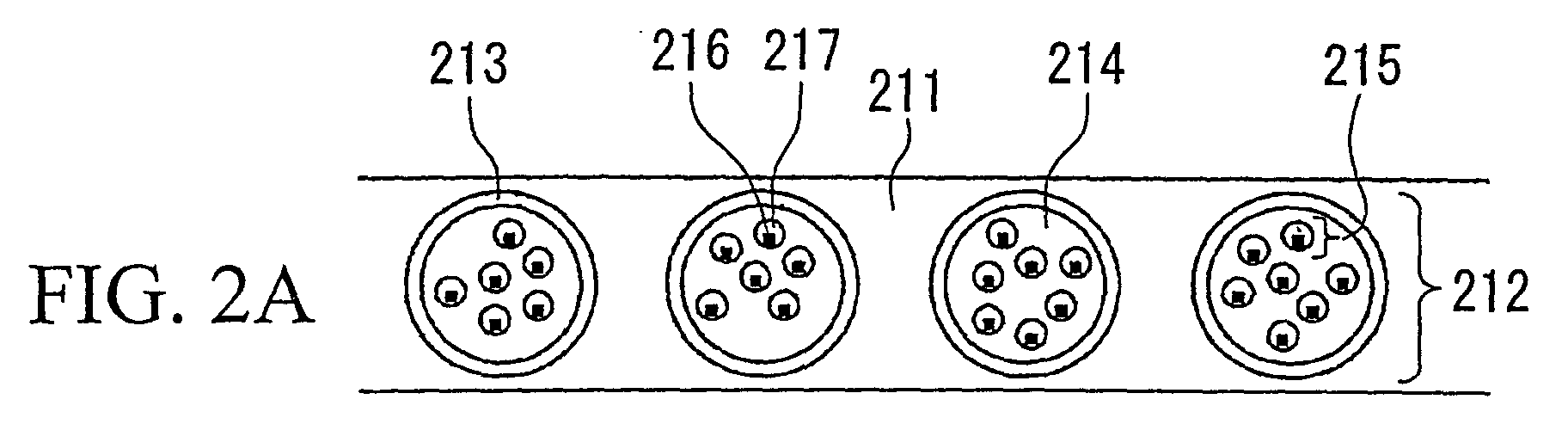
- the electrophoretic ink layer 115 is formed by a transparent binder 211 having light transmittance and plenty of microcapsules 212.
- the microcapsules 212 are distributed uniformly in the inside of the binder 211 in a fixed state.
- the thickness of the electrophoretic ink layer 115 is 1.5 to 2 times as large as external diameters of the microcapsules 212.
- As the material for the binder 211 it is possible to use silicone resin and the like.
- Each microcapsule 212 is defined by a capsule body 213 that has a hollow spherical shape and transmits light.
- the inside of the capsule body 213 is filled with liquid (or solvent) 214, in which negatively charged particles 215 are dispersed.
- Each of the charged particles 215 has a nucleus 216 that is coated with a coating layer 217.
- Each charged particle 215 and the liquid 214 mutually differ from each other in color. That is, different colors are set to them respectively. For example, the charged particles 215 are white, while the liquid 214 is blue, red, green or black. Additionally, approximately the same specific gravity is set for both of the liquid 214 and charged particles 215 within the microcapsule 212.
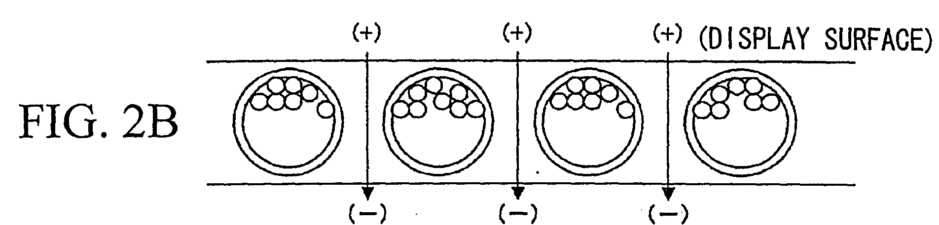
- the charged particles 215 move within the microcapsules 212 in directions opposite to the direction of the electric field. If the display surface of the display presently corresponds to an upper surface of the substrate 112 shown in FIG. 1, the charged particles 215 move upwards within the microcapsules 212 of the electrophoretic ink layer 115, which is shown in FIG. 2B. In that case, it is possible to observe the color (i.e., white) of the charged particles 215 that are floating upwards above the background color, which corresponds to the color (e.g., blue, red, green, or black) of the liquid 214.
- the color i.e., white
- the display allows only the color (e.g., blue, red, green, or black) of the liquid 214 to be observed, which is shown in FIG. 2C.
- the charged particles 215 Once the charged particles 215 are moved in directions opposite to the direction of the electric field applied to the microcapsules 212, they will likely maintain the same positions within the microcapsules 212 for a relatively long time after the electric field disappears because they have approximately the same specific gravity as that of the liquid 214.
- the electrophoretic display has a memory for retaining colors of images. Therefore, by controlling the application of an electric field with respect to each of the pixels, it is possible to provide specific electric-field application patterns, by which information is to be displayed. Once the information is displayed on the display surface of the electrophoretic display, it is maintained on the display surface for a relatively long time.
- the drive voltage (or potential difference) that is needed for changing over the display content depends upon the sizes (i.e., diameters) of the microcapsules, and it is estimated to be 1 V/ ⁇ m or so.
- the microcapsules have prescribed diameters that range within several tens of microns, for example.
- the drive voltage is estimated at 10V or so.
- the drive voltage is set to 10V in the electrophoretic display, which is driven by the known drive method typically employed by liquid crystal displays.
- the constant voltage of 10V is applied to the common electrode 113, while the prescribed voltage of 0V or 20V is applied to the pixel electrode 114.
- the prescribed voltage applied to the pixel electrode 114 (hereinafter, simply referred to as 'pixel electrode drive voltage') is set to 0V in order to increase the potential of the common electrode 113 to be higher than the potential of the pixel electrode 114.
- the pixel electrode drive voltage is set to 20V in order to increase the potential of the pixel electrode 114 to be higher than the potential of the common electrode 113. Switching over the pixel electrode drive voltage allows the electrophoretic display to rewrite its display content.
- the TFT 116 is used to switch over the pixel electrode drive voltage. In practice, however, if the electrophoretic display is driven as described above, the drive voltage is increased too high to ensure satisfactory reliability in the switching operation of the TFT 116.
- the pixel electrode drive voltage of 20V is only the least estimated voltage.
- an electrophoretic display for practical use may have an increased pixel electrode drive voltage of 30V or more. If the pixel electrode drive voltage is increased very high, it becomes more difficult to ensure satisfactory reliability in the switching operation of the TFT.
- Another typical drive method for use in liquid crystal displays is to vary the potential of the common electrode as well, which is normally called 'common voltage swing'.
- the pixel electrode drive voltage is set to 0V while the voltage applied to the common electrode (hereinafter, simply referred to as 'common electrode drive voltage') is set to 10V in order to increase the potential of the common electrode to be higher than the potential of the pixel electrode.
- the pixel electrode drive voltage is set to 10V while the common electrode drive voltage is set to 0V in order to increase the potential of the pixel electrode to be higher than the potential of the common electrode.
- Adequately switching over the pixel electrode drive voltage and common electrode drive voltage allows the electrophoretic display to rewrite its display content. Thus, it is possible to improve the reliability in the switching operation of the TFT.
- the aforementioned drive method has a problem, which will be described below.
- the common electrode drive voltage is set to 10V while the pixel electrode drive voltage is set to 0V in order to rewrite the display content with respect to a certain pixel of the display.
- the voltage of 10V should be applied to all other pixel electrodes of the display. Normally, the voltage is applied to the pixel electrodes by sequentially selecting transistors for the pixels. Therefore, it is difficult to perfectly match the voltage applying timing for the prescribed pixel electrode with the voltage applying timing for the common electrode. For this reason, a delay may be caused to occur between these timings. Due to such a delay, there is a possibility that an error will occur in rewriting the display content of the display.
- This invention provides an electrophoretic display using electrophoretic ink comprising a transparent substrate, a common electrode, pixel electrodes, and switching elements such as thin-film transistors. It is preferable to use low-temperature processed polysilicon thin-film transistors in consideration of the mobility (or portability) and the capability of incorporating drivers. In order to reduce the manufacturing cost, it is preferable that at least channels of the thin-film transistors are formed by organic films.
- An electrophoretic ink layer, which is arranged between the common electrode and pixel electrodes, is actualized by a linear arrangement of microcapsules each of which contains negatively charged white particles dispersed in a liquid having a specific color.
- the negatively charged particles move upwards or downwards within the microcapsules when being attracted to either the common electrode or the pixel electrodes under the influence of an electric field. Therefore, it is possible to observe the color of the negatively charged particles or the color of the liquid emerging on the display surface.
- All the pixel electrodes are simultaneously set to the low electric potential while the common electrode is set to the high electric potential so that the display content is erased from the entire area of the display surface at once.
- the display surface is entirely white because the negatively charged particles move upwards within the microcapsules when attracted to the common electrode.
- the pixel electrodes are driven respectively in response to display data while the common electrode is set to the low electric potential so that the display content is rewritten with a new one in response to the display data. Due to the aforementioned processes, it is possible to ensure rewriting of the display content without error.
- the negatively charged particles and the liquid are both approximately set to the same specific gravity, the negatively charged particles can maintain their positions within the microcapsules after the electric field disappears. Hence, it is possible for the display content to remain on the display surface for a relatively long time.
- FIG. 3 shows a brief appearance of an electronic book 31 employing the electrophoretic display of this invention.
- the electronic book 31 is basically constructed by a frame 32 and an open/close cover 33.
- a display 34 is installed in the frame 32 such that its display surface is exposed outside; and it is controlled by switches or buttons arranged in an area for operation controls 35.
- a controller 36, a counter 37 and a memory 38 Inside of the frame 32, there are provided a controller 36, a counter 37 and a memory 38, which are shown in FIG. 4.
- the display 34 provides a pixel array portion 39 that is formed by filling thin-film elements with electrophoretic ink, and peripheral circuits 40 whose circuit elements are integrated.
- the pixel array portion 39 and its peripheral circuits 40 are combined and unified together within the same unit of the display 34.
- the peripheral circuits 40 contain scan drivers and data drivers that operate in accordance with the prescribed decoding system.
- the peripheral circuits 40 made by integrated circuits, which are unified together with the pixel array portion 39, will be described with reference to Figures 5 to 7.
- the pixel array portion 39 is made in a matrix form defined by horizontal lines and vertical lines, namely scan lines and data lines. Therefore, the peripheral circuits 40 provide four drivers in connection with these lines of the pixel array portion 39, which is shown in FIG. 5. Specifically, a pair of data drivers 51 and 52 are connected to both ends of data lines, and a pair of scan drivers 53 and 54 are connected to both ends of scan lines.
- FIG. 6 shows a detailed circuit configuration for the data drivers 51 and 52 respectively. That is, each data driver is configured by a 9-bit decoder 61, a level shifter 62, a combination of buffers and AND gate switches 63, and analog sample-hold thin-film transistors 64.
- the decoder 61 is configured by three NAND gates and one NOR gate, which are connected with eighteen address signal lines. An output of the decoder 61 is connected to eight buffers by way of the level shifter 62. Therefore, the decoder 61 outputs an address signal simultaneously to eight data lines by way of the eight buffers and their AND gate switches 63 respectively.
- eight analog sample-hold thin film transistors 64 are simultaneously switched over in response to the address signal. As a result, eight data are simultaneously and respectively transferred to eight hold capacitors.
- the aforementioned circuit configuration is suited to reduce operation speeds of the data drivers 51 and 52.
- FIG. 7 shows a detailed circuit configuration for the scan drivers 53 and 54 respectively. That is, each scan driver comprises a 10-bit decoder 71, an interlaced switch circuit 72, a level shifter 73, and an output buffer 74.
- This circuit configuration is drawn in response to a simultaneous scan mode in which two lines are simultaneously scanned and/or a non-interlaced scan mode.
- three control signals A, B, and C are applied to the interlaced switch circuit 72.
- the data drivers 51, 52 and the scan drivers 53, 54 operate in accordance with the prescribed decoding system. Therefore, the pixel array portion 39 is merely required to control the electrophoretic ink layer 115 in such a manner that the display content is rewritten with respect to the pixel for which display data is to be updated. This guarantees reduction of power consumption by the electrophoretic display when it is used in an electronic book.
- the controller 36 shown in FIG. 4 performs a display content rewriting process in accordance with a flowchart of FIG. 8.
- the controller 36 erases all display data that have been displayed over an entire area of the display surface.
- all the pixel electrodes are set to the same electric potential (e.g., ground potential or Vss), then, 'positive' voltages are applied to the common electrode.
- Vss ground potential
- the display 34 proceeds to rewriting old display contents with new ones on the display surface. That is, the controller 36 reads new display data from the memory 38; then, it issues instructions to write the new display data to the electrophoretic ink layer 115 with respect to pixels of the pixel array portion 39 respectively. Specifically, the ground potential or Vss is applied to the common electrode 113; then, the controller 36 proceeds to selection of pixels by means of the aforementioned drivers 51 to 54 of the prescribed decoding system, so that the new display data are to be rewritten with respect to the pixel electrodes 114 respectively.
- low voltage corresponding to the same voltage (e.g., ground potential or Vss) of the common electrode 113 is applied to the pixel electrodes 114.
- high voltage that is 'positive' as compared with the electric potential of the common electrode 113 is applied to the pixel electrodes 114.
- the controller 36 selects only the pixels that are used to display the black color, to which display data are to be written, without selecting other pixels that are used to display the white color.
- This method can be easily realized by using the aforementioned drivers 51 to 54 of the prescribed decoding system.
- Using the electrophoretic ink it is possible to actualize a display of a reflection type having a high contrast ratio.
- this display can reduce consumption of electricity because it does not require the back light.
- the aforementioned process is executed every time the display 34 rewrites its display content on the display surface.
- the display using the electrophoretic ink can be easily applied to electronic books because it has memory for retaining its display content for a while.
- the aforementioned drive method is preferable for use in electronic books using electrophoretic displays.
- the low-temperature processed polysilicon thin-film transistors for the electrophoretic display of this invention.
- at least channels of thin-film transistors are formed by organic films in order to further reduce the manufacturing cost.
- the electrophoretic display of this invention is not necessarily limited to the aforementioned embodiment corresponding to the electronic book, hence, it is possible to propose a variety of modifications.
- the electrophoretic display provides 'colored' visual representations instead of 'monochrome' visual representations.
- the monochrome display is actualized using a single thin-film transistor with respect to each pixel as shown in FIG. 1.
- the color display is actualized using three thin-film transistors with respect to each pixel, which is shown in FIG. 9. That is, an entire area of the electrophoretic ink layer 115, which is arranged between the common electrode 113 and the pixel electrode 114, is partitioned into three layers by intervention of two banks 93 respectively.
- the partitioned three layers are named a cyan-color electrophoretic ink layer 115C, a magenta-color electrophoretic ink layer 115M, and a yellow-color electrophoretic ink layer 115Y, which are arranged below the common electrode 113 and in connection with the divided three portions of the pixel electrode 114.
- the divided three portions of the pixel electrode 114 are respectively controlled in switching voltage by three thin-film transistors respectively. Therefore, a combination of the three electrophoretic ink layers 115C, 115M and 115Y that are respectively controlled in switching voltage by a combination of the three thin-film transistors is used to form one color pixel for the electrophoretic display.
- the electrophoretic display of this invention is applicable to a variety of electronic devices having displays; therefore, the application of this invention is not necessarily limited to electronic books, an example of which is described as the foregoing embodiment. Next, descriptions will be given with respect to other examples of the electronic devices, each of which is able to use the electrophoretic display of this invention.
- FIG. 10 shows an external appearance of a personal computer 1100, which basically comprises a main unit 1104 providing a keyboard 1102, and a display unit whose display 100 corresponds to the electrophoretic display.
- FIG. 11 shows an external appearance of a cellular phone 1200, which basically comprises numeric keys and function keys 1202, an earpiece 1204, a mouthpiece 1206, and a small-size display 100 that corresponds to the electrophoretic display.
- FIG. 12 shows a backside appearance of a digital still camera 1300 and its connections to external devices.
- Normal cameras are designed to provide exposures on films in response to optical images of photographed subjects.
- the digital still camera 1300 uses an image pickup device such as a CCD (i.e., Charge Coupled Device) to pick up an optical image of a photographed subject, based on which image pickup signals representing a photographed image are produced by photoelectric conversion.
- a display 100 corresponding to the electrophoretic display is arranged at a prescribed area of a backside surface of a case 1302 of the digital still camera 1300. This display 100 displays pictures that are produced based on image pickup signals for a viewer. That is, the display 100 acts as a viewfinder for a photographer.
- a light sensing unit is embedded in the backside of the case 1302 to provide various parts for optics such as optical lenses and a CCD.
- the CCD When a photographer pushes a shutter button 1306 while watching a photographed subject that is displayed on a screen of the display 100, the CCD produces image pickup signals, representing a photographed image, which are transferred and stored in a memory on a circuit board 1308 embedded in the backside of the case 1302 at its right area.
- the digital still camera 1300 provides video signal output terminals 1312 and an input/output terminal 1314 for data communication. Therefore, it is possible to connect the digital still camera 1300 with a television monitor 1430 by way of cables connected to the video signal output terminals 1312. In addition, it is possible to connect the digital still camera 1300 with a personal computer 1440 by way of a data communication cable connected to the input/output terminal 1314.
- FIG. 13 shows an external appearance of an electronic paper 1400, which basically comprises a rewritable sheet 1401 that has similar touch and flexibility of conventional papers, and a display 100 corresponding to the electrophoretic display.
- FIG. 14 shows an external appearance of an electronic notebook 1402 in which a number of electronic papers 1400 are bound together with a note cover 1403.
- the note cover 1403 provides a display data input device (not shown) that is used to input display data from the external device. In response to the display data, it is possible to change or update the display content with respect to each of the electronic papers 1400 bound together with the note cover 1403.
- electrophoretic display such as the electronic book of FIG. 3, the personal computer of FIG. 10, the cellular phone of FIG. 11, the digital still camera of FIG. 12, and the electronic paper of FIG. 13.
- liquid crystal display television set videotape recorder of the viewfinder type or monitor type
- car navigation device pager
- electronic picket notebook electronic calculator
- word processor workstation
- television phone POS terminal
- other devices having touch panels such as the liquid crystal display television set, videotape recorder of the viewfinder type or monitor type, car navigation device, pager, electronic picket notebook, electronic calculator, word processor, workstation, television phone, POS terminal, and other devices having touch panels.
- the electrophoretic display of this invention can be used as displays for the aforementioned devices.
- this invention has a variety of technical features and effects, which are described below.
Landscapes
- Physics & Mathematics (AREA)
- Engineering & Computer Science (AREA)
- General Physics & Mathematics (AREA)
- Nonlinear Science (AREA)
- Chemical Kinetics & Catalysis (AREA)
- Molecular Biology (AREA)
- Electrochemistry (AREA)
- Health & Medical Sciences (AREA)
- Chemical & Material Sciences (AREA)
- Optics & Photonics (AREA)
- Life Sciences & Earth Sciences (AREA)
- Computer Hardware Design (AREA)
- Theoretical Computer Science (AREA)
- Electrochromic Elements, Electrophoresis, Or Variable Reflection Or Absorption Elements (AREA)
- Control Of Indicators Other Than Cathode Ray Tubes (AREA)
Abstract
Description
Claims (15)
- An electrophoretic display comprising:wherein the common electrode and the pixel electrodes are respectively driven at different electric potentials causing electric fields by which the charged pigment particles move in desired directions to form a desired display content emerging above the display surface in response to display data, which is rewritten in such a manner that the display content is erased at once from the entire area corresponding to the display surface and is then rewritten with a new one.a plurality of pixel electrodes (114) that are provided independently with respect to pixels uniformly arranged above a display surface;an active-matrix array of switching elements (116) that are respectively connected with the pixel electrodes;a substrate (112) having a common electrode (113) that covers an entire area corresponding to the display surface; andan electrophoretic ink layer (115) in which a number of charged pigment particles (215) are contained and dispersed in dyed solution (214),
- An electrophoretic display according to claim 1, wherein a first common voltage being applied to the common electrode to erase the display content from the entire area corresponding to the display surface, while a second common voltage is alternatively applied to the common electrode to rewrite the display content with the new one.
- An electrophoretic display according to claim 1 or 2, wherein voltages respectively applied to the common electrode and the pixel electrodes being both not greater than 20V.
- An electrophoretic display according to claim 1 or 2, wherein voltages respectively applied to the common electrode and the pixel electrodes being both not greater than 15V.
- An electrophoretic display according to claim 1 or 2, wherein voltages respectively applied to the common electrode and the pixel electrodes being both not greater than 10V.
- An electrophoretic display according to claim 1 or 2, wherein the charged pigment particles and the dyed solution being contained in a plurality of microcapsules, which are linearly arranged within the electrophoretic ink layer.
- An electrophoretic display according to claim 1 or 2, wherein the switching elements comprising thin-film transistors.
- An electrophoretic display according to claim 7, wherein the thin-film transistors being low-temperature processed polysilicon thin-film transistors.
- An electrophoretic display according to claim 7, wherein at least channels of the thin-film transistors being made by organic films.
- An electrophoretic display according to claim 1 or 2, wherein the display content being erased from the entire area corresponding to the display surface in such a manner that a prescribed voltage is applied between the common electrode and the pixel electrodes while all the pixel electrodes are commonly set to a same electric potential.
- An electrophoretic display according to claim 10, wherein an absolute value of an electric potential of the common electrode being normally set lower than absolute values of electric potentials of the pixel electrodes in order to rewrite the display content with the new one.
- An electrophoretic display according to claim 10, wherein a reference color being defined when an absolute value of an electric potential of the common electrode being set higher than absolute values of electric potentials of the pixel electrodes.
- An electronic apparatus having the electrophoretic display as defined in claim 1 or 2.
- An electrophoretic display comprising:a transparent substrate (112) that forms a display surface;a common electrode (113) that covers an entire area corresponding to the display surface;a plurality of pixel electrodes (114) that are arranged under the common electrode and in connection with pixels respectively;a plurality of thin-film transistors (116) whose drain electrodes are connected to the plurality of pixel electrodes respectively, so that each of the pixel electrodes is independently controlled in electric potential by switching each of the thin-film transistors; andan electrophoretic ink layer (115) that contains a plurality of microcapsules linearly arranged between the common electrode and the pixel electrodes, wherein each of the microcapsules containing a number of negatively charged particles (215) having white colors dispersed in a liquid (214) having its specific color, and wherein both of the negatively charged particles and the liquid being set to approximately a same specific gravity within the microcapsule.
- An electrophoretic display according to claim 14, wherein all of the pixel electrodes being simultaneously set to a low electric potential while the common electrode being set to a high electric potential so that a display content is erased from the entire area corresponding to the display surface at once, and then the pixel electrodes being driven respectively in response to display data while the common electrode being set to the low electric potential so that the display content is rewritten with a new one in response to the display data.
Priority Applications (1)
| Application Number | Priority Date | Filing Date | Title |
|---|---|---|---|
| EP08010649.5A EP1968041B1 (en) | 2000-08-31 | 2001-08-30 | Active matrix electrophoretic display device |
Applications Claiming Priority (4)
| Application Number | Priority Date | Filing Date | Title |
|---|---|---|---|
| JP2000263565 | 2000-08-31 | ||
| JP2000263565 | 2000-08-31 | ||
| JP2001233811 | 2001-08-01 | ||
| JP2001233811A JP3719172B2 (en) | 2000-08-31 | 2001-08-01 | Display device and electronic device |
Related Child Applications (1)
| Application Number | Title | Priority Date | Filing Date |
|---|---|---|---|
| EP08010649.5A Division EP1968041B1 (en) | 2000-08-31 | 2001-08-30 | Active matrix electrophoretic display device |
Publications (3)
| Publication Number | Publication Date |
|---|---|
| EP1184714A2 true EP1184714A2 (en) | 2002-03-06 |
| EP1184714A3 EP1184714A3 (en) | 2003-09-17 |
| EP1184714B1 EP1184714B1 (en) | 2008-07-30 |
Family
ID=26598966
Family Applications (2)
| Application Number | Title | Priority Date | Filing Date |
|---|---|---|---|
| EP01307375A Expired - Lifetime EP1184714B1 (en) | 2000-08-31 | 2001-08-30 | Electrophoretic display and driving method |
| EP08010649.5A Expired - Lifetime EP1968041B1 (en) | 2000-08-31 | 2001-08-30 | Active matrix electrophoretic display device |
Family Applications After (1)
| Application Number | Title | Priority Date | Filing Date |
|---|---|---|---|
| EP08010649.5A Expired - Lifetime EP1968041B1 (en) | 2000-08-31 | 2001-08-30 | Active matrix electrophoretic display device |
Country Status (6)
| Country | Link |
|---|---|
| US (1) | US6987503B2 (en) |
| EP (2) | EP1184714B1 (en) |
| JP (1) | JP3719172B2 (en) |
| CN (1) | CN1150506C (en) |
| DE (1) | DE60135071D1 (en) |
| TW (1) | TW538263B (en) |
Cited By (6)
| Publication number | Priority date | Publication date | Assignee | Title |
|---|---|---|---|---|
| WO2007004120A3 (en) * | 2005-06-30 | 2007-05-03 | Koninkl Philips Electronics Nv | Cross talk reduction in electrophoretic displays |
| WO2008059039A1 (en) * | 2006-11-16 | 2008-05-22 | Liquavista B.V. | Driving of electro-optic displays |
| CN100422836C (en) * | 2004-02-03 | 2008-10-01 | 兄弟工业株式会社 | electronic notebook |
| CN100432818C (en) * | 2003-06-24 | 2008-11-12 | 精工爱普生株式会社 | Electrophoresis dispersion, electrophoresis display device, manufacturing method thereof and electronic machine |
| US7701435B2 (en) | 2004-03-29 | 2010-04-20 | Seiko Epson Corporation | Electrophoretic display, method for driving electrophoretic display, and storage display |
| US8569758B2 (en) | 2008-12-24 | 2013-10-29 | Boe Technology Group Co., Ltd. | Touching-type electronic paper and method for manufacturing the same |
Families Citing this family (175)
| Publication number | Priority date | Publication date | Assignee | Title |
|---|---|---|---|---|
| JP3925080B2 (en) * | 2000-12-01 | 2007-06-06 | セイコーエプソン株式会社 | Electronic book and method of manufacturing electronic paper used therefor |
| AU2002250304A1 (en) * | 2001-03-13 | 2002-09-24 | E Ink Corporation | Apparatus for displaying drawings |
| US7492505B2 (en) * | 2001-08-17 | 2009-02-17 | Sipix Imaging, Inc. | Electrophoretic display with dual mode switching |
| US7038670B2 (en) * | 2002-08-16 | 2006-05-02 | Sipix Imaging, Inc. | Electrophoretic display with dual mode switching |
| TW550529B (en) * | 2001-08-17 | 2003-09-01 | Sipix Imaging Inc | An improved electrophoretic display with dual-mode switching |
| JP4785300B2 (en) * | 2001-09-07 | 2011-10-05 | 株式会社半導体エネルギー研究所 | Electrophoretic display device, display device, and electronic device |
| JP4027178B2 (en) * | 2001-09-12 | 2007-12-26 | キヤノン株式会社 | Electrophoretic display device |
| EP1512044A1 (en) * | 2002-05-24 | 2005-03-09 | Koninklijke Philips Electronics N.V. | Electrophoretic display device and driving method therefor |
| JP4651383B2 (en) * | 2002-06-13 | 2011-03-16 | イー インク コーポレイション | Method for driving electro-optic display device |
| JP2004024383A (en) * | 2002-06-24 | 2004-01-29 | Sony Corp | Electronics |
| US7640293B2 (en) * | 2002-07-17 | 2009-12-29 | Research In Motion Limited | Method, system and apparatus for messaging between wireless mobile terminals and networked computers |
| JP3942975B2 (en) * | 2002-07-18 | 2007-07-11 | シャープ株式会社 | Image reading apparatus and image forming apparatus having the same |
| US7038656B2 (en) * | 2002-08-16 | 2006-05-02 | Sipix Imaging, Inc. | Electrophoretic display with dual-mode switching |
| US7271947B2 (en) * | 2002-08-16 | 2007-09-18 | Sipix Imaging, Inc. | Electrophoretic display with dual-mode switching |
| KR20050049526A (en) * | 2002-10-10 | 2005-05-25 | 코닌클리케 필립스 일렉트로닉스 엔.브이. | Electrophoretic display panel |
| AU2003260855A1 (en) * | 2002-10-16 | 2004-05-04 | Koninklijke Philips Electronics N.V. | A display apparatus with a display device and method of driving the display device |
| CN100361017C (en) * | 2002-10-21 | 2008-01-09 | 西北工业大学 | White electronic ink microcapsules |
| JP4529350B2 (en) * | 2002-11-13 | 2010-08-25 | セイコーエプソン株式会社 | Electro-optical device and electronic apparatus |
| AU2003233105A1 (en) * | 2003-01-23 | 2004-08-13 | Koninklijke Philips Electronics N.V. | Electrophoretic display device and driving method therefor |
| US20040174335A1 (en) * | 2003-03-03 | 2004-09-09 | Lee Wang | Driver control scheme for electronic-ink display |
| WO2004079705A1 (en) * | 2003-03-07 | 2004-09-16 | Koninklijke Philips Electronics N.V. | Electrophoretic display panel |
| CN101387809A (en) * | 2003-05-02 | 2009-03-18 | 伊英克公司 | Electrophoretic medium and display containing the electrophoretic medium |
| EP1656658A4 (en) * | 2003-08-19 | 2009-12-30 | E Ink Corp | Methods for controlling electro-optic displays |
| US20050263903A1 (en) * | 2003-08-30 | 2005-12-01 | Visible Tech-Knowledgy, Inc. | Method for pattern metalization of substrates |
| CN100557676C (en) * | 2003-09-12 | 2009-11-04 | 皇家飞利浦电子股份有限公司 | Method of compensating temperature dependence of electrophoretic display drive scheme |
| WO2005029458A1 (en) * | 2003-09-19 | 2005-03-31 | E Ink Corporation | Methods for reducing edge effects in electro-optic displays |
| US20070002009A1 (en) * | 2003-10-07 | 2007-01-04 | Pasch Nicholas F | Micro-electromechanical display backplane and improvements thereof |
| US8928562B2 (en) * | 2003-11-25 | 2015-01-06 | E Ink Corporation | Electro-optic displays, and methods for driving same |
| US6977766B2 (en) * | 2004-01-14 | 2005-12-20 | Hewlett-Packard Development Company, L.P. | Display device with side-illuminated cell |
| JP4151591B2 (en) * | 2004-03-09 | 2008-09-17 | セイコーエプソン株式会社 | Display device and display device information erasing method |
| TW200625223A (en) * | 2004-04-13 | 2006-07-16 | Koninkl Philips Electronics Nv | Electrophoretic display with rapid drawing mode waveform |
| US20050253803A1 (en) * | 2004-05-13 | 2005-11-17 | Xerox Corporation | Electric paper display with a thin film transistor active matrix and integrated addressing logic |
| US20050253802A1 (en) * | 2004-05-14 | 2005-11-17 | Wright Charles A | Gyricon media using amorphous silicon thin film transistor active matrix arrays and a refresh method for the same |
| DE102004037365B4 (en) * | 2004-07-30 | 2011-12-01 | Deutsche Post Ag | Containers with electronic labels; Use of an electronic label for labeling containers |
| CN101859544B (en) * | 2004-08-13 | 2012-07-04 | 伊英克公司 | Method and apparatus for driving electro-optic display |
| US8643595B2 (en) * | 2004-10-25 | 2014-02-04 | Sipix Imaging, Inc. | Electrophoretic display driving approaches |
| US20060146271A1 (en) * | 2005-01-04 | 2006-07-06 | Pennaz Thomas J | Universal display module |
| JP4718859B2 (en) | 2005-02-17 | 2011-07-06 | セイコーエプソン株式会社 | Electrophoresis apparatus, driving method thereof, and electronic apparatus |
| JP4483639B2 (en) * | 2005-03-18 | 2010-06-16 | セイコーエプソン株式会社 | Electrophoretic display device and driving method thereof |
| JP4419944B2 (en) * | 2005-03-29 | 2010-02-24 | セイコーエプソン株式会社 | Electrophoretic display device and driving method thereof |
| CN100456118C (en) * | 2005-03-29 | 2009-01-28 | 精工爱普生株式会社 | Electrophoretic display device |
| EP1742194A1 (en) * | 2005-07-04 | 2007-01-10 | Seiko Epson Corporation | Electro-optical display and method of operation |
| EP1742195A1 (en) * | 2005-07-04 | 2007-01-10 | Seiko Epson Corporation | Electrochromic display and method of operation |
| GB0515175D0 (en) | 2005-07-25 | 2005-08-31 | Plastic Logic Ltd | Flexible resistive touch screen |
| US20080259057A1 (en) * | 2005-09-14 | 2008-10-23 | Johannes Brons | Electronic Reading Device Mimicking a Reading experience of a Paper Document |
| US20070069995A1 (en) * | 2005-09-28 | 2007-03-29 | Shin Hyun S | Flat panel display and a method of driving the same |
| KR101281885B1 (en) | 2005-11-18 | 2013-07-03 | 엘지디스플레이 주식회사 | electrophoretic display device |
| TWI380114B (en) * | 2005-12-15 | 2012-12-21 | Nlt Technologies Ltd | Electrophoretic display device and driving method for same |
| KR101163605B1 (en) | 2005-12-30 | 2012-07-06 | 엘지디스플레이 주식회사 | Display device of electronic ink type and method for driving the same |
| TWI344133B (en) * | 2006-02-24 | 2011-06-21 | Prime View Int Co Ltd | Thin film transistor array substrate and electronic ink display device |
| TW200732808A (en) | 2006-02-24 | 2007-09-01 | Prime View Int Co Ltd | Thin film transistor array substrate and electronic ink display device |
| JP5348363B2 (en) * | 2006-04-25 | 2013-11-20 | セイコーエプソン株式会社 | Electrophoretic display device, electrophoretic display device driving method, and electronic apparatus |
| GB0611032D0 (en) * | 2006-06-05 | 2006-07-12 | Plastic Logic Ltd | Multi-touch active display keyboard |
| US7675672B2 (en) * | 2006-11-09 | 2010-03-09 | Honeywell International Inc. | Non-volatile addressable electronic paper for disposable flexible displays |
| KR101432804B1 (en) * | 2006-12-13 | 2014-08-27 | 엘지디스플레이 주식회사 | Electrophoretic display device and driving method thereof |
| JP5369375B2 (en) * | 2006-12-27 | 2013-12-18 | セイコーエプソン株式会社 | Display device and electronic paper |
| JP4345820B2 (en) * | 2007-01-22 | 2009-10-14 | セイコーエプソン株式会社 | Display device, display device manufacturing method, and electronic paper |
| JP4269187B2 (en) | 2007-01-25 | 2009-05-27 | セイコーエプソン株式会社 | Electrophoresis device, electrophoretic device driving method, and electronic apparatus |
| US8274472B1 (en) | 2007-03-12 | 2012-09-25 | Sipix Imaging, Inc. | Driving methods for bistable displays |
| US8243013B1 (en) | 2007-05-03 | 2012-08-14 | Sipix Imaging, Inc. | Driving bistable displays |
| US20080303780A1 (en) | 2007-06-07 | 2008-12-11 | Sipix Imaging, Inc. | Driving methods and circuit for bi-stable displays |
| KR20090003643A (en) * | 2007-07-03 | 2009-01-12 | 삼성전자주식회사 | Driving device of display device and electrophoretic display device including the same |
| JP5157322B2 (en) | 2007-08-30 | 2013-03-06 | セイコーエプソン株式会社 | Electrophoretic display device, electrophoretic display device driving method, and electronic apparatus |
| JP5071000B2 (en) * | 2007-08-31 | 2012-11-14 | セイコーエプソン株式会社 | Electrophoretic display device driving method, electrophoretic display device, and electronic apparatus |
| WO2009049204A1 (en) * | 2007-10-12 | 2009-04-16 | Sipix Imaging, Inc. | Approach to adjust driving waveforms for a display device |
| JP5019177B2 (en) | 2007-10-16 | 2012-09-05 | セイコーエプソン株式会社 | Electrophoretic display device, electronic apparatus, and driving method of electrophoretic display device |
| US8169690B2 (en) * | 2008-02-21 | 2012-05-01 | Sipix Imaging, Inc. | Color display devices |
| JP5151547B2 (en) * | 2008-02-27 | 2013-02-27 | セイコーエプソン株式会社 | Image rewriting control device and information display device |
| JP5163182B2 (en) * | 2008-02-27 | 2013-03-13 | セイコーエプソン株式会社 | Image rewriting control device and information display device |
| JP5504567B2 (en) * | 2008-03-14 | 2014-05-28 | セイコーエプソン株式会社 | Electrophoretic display device driving method, electrophoretic display device, and electronic apparatus |
| CN101540142A (en) * | 2008-03-18 | 2009-09-23 | 精工爱普生株式会社 | Electrophoretic display device driving circuit, electrophoretic display device, and electronic apparatus |
| JP5262211B2 (en) | 2008-03-19 | 2013-08-14 | セイコーエプソン株式会社 | Electrophoretic display device driving method, electrophoretic display device, and electronic apparatus |
| JP5125974B2 (en) * | 2008-03-24 | 2013-01-23 | セイコーエプソン株式会社 | Electrophoretic display device driving method, electrophoretic display device, and electronic apparatus |
| US8422116B2 (en) * | 2008-04-03 | 2013-04-16 | Sipix Imaging, Inc. | Color display devices |
| US8462102B2 (en) * | 2008-04-25 | 2013-06-11 | Sipix Imaging, Inc. | Driving methods for bistable displays |
| CN102016970B (en) * | 2008-05-01 | 2014-04-16 | 希毕克斯影像有限公司 | Color display devices |
| JP2010020231A (en) * | 2008-07-14 | 2010-01-28 | Seiko Epson Corp | Electrophoretic display device and electronic apparatus |
| FI20085737A7 (en) * | 2008-07-21 | 2010-01-22 | Oesterbacka Ronald | Components and circuit arrangements with at least one organic field effect transistor |
| JP5790968B2 (en) * | 2008-08-18 | 2015-10-07 | Nltテクノロジー株式会社 | Display device and manufacturing method thereof |
| JP2010072194A (en) * | 2008-09-17 | 2010-04-02 | Seiko Epson Corp | Display device and program |
| US8368760B1 (en) * | 2008-10-16 | 2013-02-05 | Raytheon Company | System and method to generate and display target patterns |
| US8558855B2 (en) * | 2008-10-24 | 2013-10-15 | Sipix Imaging, Inc. | Driving methods for electrophoretic displays |
| US9019318B2 (en) * | 2008-10-24 | 2015-04-28 | E Ink California, Llc | Driving methods for electrophoretic displays employing grey level waveforms |
| JP5304183B2 (en) * | 2008-11-10 | 2013-10-02 | セイコーエプソン株式会社 | Electrophoretic display device driving method, electrophoretic display device, and electronic apparatus |
| JP5277905B2 (en) * | 2008-11-27 | 2013-08-28 | セイコーエプソン株式会社 | Electrophoretic display device driving method, electrophoretic display device, and electronic apparatus |
| US8797258B2 (en) * | 2008-12-30 | 2014-08-05 | Sipix Imaging, Inc. | Highlight color display architecture using enhanced dark state |
| US8503063B2 (en) * | 2008-12-30 | 2013-08-06 | Sipix Imaging, Inc. | Multicolor display architecture using enhanced dark state |
| US20100194789A1 (en) * | 2009-01-30 | 2010-08-05 | Craig Lin | Partial image update for electrophoretic displays |
| US9251736B2 (en) | 2009-01-30 | 2016-02-02 | E Ink California, Llc | Multiple voltage level driving for electrophoretic displays |
| US8964282B2 (en) | 2012-10-02 | 2015-02-24 | E Ink California, Llc | Color display device |
| US8717664B2 (en) | 2012-10-02 | 2014-05-06 | Sipix Imaging, Inc. | Color display device |
| US20100194733A1 (en) * | 2009-01-30 | 2010-08-05 | Craig Lin | Multiple voltage level driving for electrophoretic displays |
| JP5459592B2 (en) * | 2009-03-19 | 2014-04-02 | セイコーエプソン株式会社 | Electro-optical device, driving method thereof, and electronic apparatus |
| US9460666B2 (en) * | 2009-05-11 | 2016-10-04 | E Ink California, Llc | Driving methods and waveforms for electrophoretic displays |
| US8576164B2 (en) * | 2009-10-26 | 2013-11-05 | Sipix Imaging, Inc. | Spatially combined waveforms for electrophoretic displays |
| CN101699342B (en) * | 2009-11-12 | 2012-05-23 | 友达光电股份有限公司 | Electrophoretic display panel |
| TWI392949B (en) * | 2009-11-16 | 2013-04-11 | Au Optronics Corp | Electrophoresis display panel |
| US8928641B2 (en) | 2009-12-02 | 2015-01-06 | Sipix Technology Inc. | Multiplex electrophoretic display driver circuit |
| KR101640816B1 (en) * | 2009-12-24 | 2016-07-20 | 엘지디스플레이 주식회사 | Electrophoretic display device and method for fabricating the same |
| US11049463B2 (en) * | 2010-01-15 | 2021-06-29 | E Ink California, Llc | Driving methods with variable frame time |
| US8558786B2 (en) * | 2010-01-20 | 2013-10-15 | Sipix Imaging, Inc. | Driving methods for electrophoretic displays |
| US20110217639A1 (en) * | 2010-03-02 | 2011-09-08 | Sprague Robert A | Electrophoretic display fluid |
| JP5454238B2 (en) | 2010-03-08 | 2014-03-26 | セイコーエプソン株式会社 | Electro-optic device |
| US9224338B2 (en) * | 2010-03-08 | 2015-12-29 | E Ink California, Llc | Driving methods for electrophoretic displays |
| US8633889B2 (en) | 2010-04-15 | 2014-01-21 | Semiconductor Energy Laboratory Co., Ltd. | Display device, driving method thereof, and electronic appliance |
| US9140952B2 (en) | 2010-04-22 | 2015-09-22 | E Ink California, Llc | Electrophoretic display with enhanced contrast |
| TWI534773B (en) | 2010-04-23 | 2016-05-21 | 半導體能源研究所股份有限公司 | Display device driving method |
| US9116412B2 (en) | 2010-05-26 | 2015-08-25 | E Ink California, Llc | Color display architecture and driving methods |
| US8704756B2 (en) | 2010-05-26 | 2014-04-22 | Sipix Imaging, Inc. | Color display architecture and driving methods |
| US9104082B2 (en) * | 2011-06-29 | 2015-08-11 | Hewlett-Packard Development Company, L.P. | Electronic paper with porous standoff layer |
| US9013394B2 (en) | 2010-06-04 | 2015-04-21 | E Ink California, Llc | Driving method for electrophoretic displays |
| JP5830276B2 (en) | 2010-06-25 | 2015-12-09 | 株式会社半導体エネルギー研究所 | Display device |
| JP5640552B2 (en) * | 2010-08-23 | 2014-12-17 | セイコーエプソン株式会社 | Control device, display device, and control method of display device |
| KR101323049B1 (en) * | 2010-11-09 | 2013-10-29 | 엘지디스플레이 주식회사 | Electrophoresis display device and power control method thereof |
| TWI598672B (en) | 2010-11-11 | 2017-09-11 | 希畢克斯幻像有限公司 | Driving method for electrophoretic displays |
| US8670174B2 (en) | 2010-11-30 | 2014-03-11 | Sipix Imaging, Inc. | Electrophoretic display fluid |
| US9146439B2 (en) | 2011-01-31 | 2015-09-29 | E Ink California, Llc | Color electrophoretic display |
| US10514583B2 (en) | 2011-01-31 | 2019-12-24 | E Ink California, Llc | Color electrophoretic display |
| US8786935B2 (en) | 2011-06-02 | 2014-07-22 | Sipix Imaging, Inc. | Color electrophoretic display |
| US9013783B2 (en) | 2011-06-02 | 2015-04-21 | E Ink California, Llc | Color electrophoretic display |
| CN102221973B (en) * | 2011-06-28 | 2013-02-13 | 鸿富锦精密工业(深圳)有限公司 | Electronic book reader and flipping-over control method thereof |
| US8605354B2 (en) | 2011-09-02 | 2013-12-10 | Sipix Imaging, Inc. | Color display devices |
| US8649084B2 (en) | 2011-09-02 | 2014-02-11 | Sipix Imaging, Inc. | Color display devices |
| US8917439B2 (en) | 2012-02-09 | 2014-12-23 | E Ink California, Llc | Shutter mode for color display devices |
| US8797636B2 (en) | 2012-07-17 | 2014-08-05 | Sipix Imaging, Inc. | Light-enhancing structure for electrophoretic display |
| US10907938B2 (en) | 2012-08-17 | 2021-02-02 | Raytheon Company | Infrared camouflage textile |
| US11017705B2 (en) | 2012-10-02 | 2021-05-25 | E Ink California, Llc | Color display device including multiple pixels for driving three-particle electrophoretic media |
| US9360733B2 (en) | 2012-10-02 | 2016-06-07 | E Ink California, Llc | Color display device |
| CN104144791A (en) * | 2012-10-09 | 2014-11-12 | 阿肯马法国公司 | Multi-color electrophoretic ink, related display device and manufacturing method |
| US9502193B2 (en) | 2012-10-30 | 2016-11-22 | Apple Inc. | Low-travel key mechanisms using butterfly hinges |
| US9710069B2 (en) | 2012-10-30 | 2017-07-18 | Apple Inc. | Flexible printed circuit having flex tails upon which keyboard keycaps are coupled |
| US9449772B2 (en) | 2012-10-30 | 2016-09-20 | Apple Inc. | Low-travel key mechanisms using butterfly hinges |
| HK1217548A1 (en) * | 2013-02-06 | 2017-01-13 | Apple Inc. | Input/output device with a dynamically adjustable appearance and function |
| WO2014172636A1 (en) | 2013-04-18 | 2014-10-23 | Sipix Imaging, Inc. | Color display device |
| CA2912689C (en) | 2013-05-17 | 2019-08-20 | E Ink California, Llc | Color display device |
| WO2014186605A1 (en) | 2013-05-17 | 2014-11-20 | Sipix Imaging, Inc. | Color display device with color filters |
| US9383623B2 (en) | 2013-05-17 | 2016-07-05 | E Ink California, Llc | Color display device |
| US9412533B2 (en) | 2013-05-27 | 2016-08-09 | Apple Inc. | Low travel switch assembly |
| US20140362066A1 (en) * | 2013-06-07 | 2014-12-11 | Delta Electronics, Inc. | Method of driving an information display panel |
| US9908310B2 (en) | 2013-07-10 | 2018-03-06 | Apple Inc. | Electronic device with a reduced friction surface |
| JP6273730B2 (en) * | 2013-09-18 | 2018-02-07 | セイコーエプソン株式会社 | Electrophoretic display device and electronic apparatus |
| JP2016532232A (en) | 2013-09-30 | 2016-10-13 | アップル インコーポレイテッド | Key cap with reduced thickness |
| WO2015047606A1 (en) | 2013-09-30 | 2015-04-02 | Apple Inc. | Keycaps having reduced thickness |
| US10380931B2 (en) | 2013-10-07 | 2019-08-13 | E Ink California, Llc | Driving methods for color display device |
| US10726760B2 (en) | 2013-10-07 | 2020-07-28 | E Ink California, Llc | Driving methods to produce a mixed color state for an electrophoretic display |
| TWI550332B (en) | 2013-10-07 | 2016-09-21 | 電子墨水加利福尼亞有限責任公司 | Driving methods for color display device |
| TWI534520B (en) | 2013-10-11 | 2016-05-21 | 電子墨水加利福尼亞有限責任公司 | Color display device |
| PL3095007T3 (en) | 2014-01-14 | 2020-10-05 | E Ink California, Llc | Method of driving a color display layer |
| US9541814B2 (en) | 2014-02-19 | 2017-01-10 | E Ink California, Llc | Color display device |
| US20150268531A1 (en) | 2014-03-18 | 2015-09-24 | Sipix Imaging, Inc. | Color display device |
| US9779889B2 (en) | 2014-03-24 | 2017-10-03 | Apple Inc. | Scissor mechanism features for a keyboard |
| US9704665B2 (en) | 2014-05-19 | 2017-07-11 | Apple Inc. | Backlit keyboard including reflective component |
| US10891906B2 (en) | 2014-07-09 | 2021-01-12 | E Ink California, Llc | Color display device and driving methods therefor |
| US10380955B2 (en) | 2014-07-09 | 2019-08-13 | E Ink California, Llc | Color display device and driving methods therefor |
| WO2016025890A1 (en) | 2014-08-15 | 2016-02-18 | Apple Inc. | Fabric keyboard |
| US10082880B1 (en) | 2014-08-28 | 2018-09-25 | Apple Inc. | System level features of a keyboard |
| WO2016053911A2 (en) | 2014-09-30 | 2016-04-07 | Apple Inc. | Venting system and shield for keyboard assembly |
| US10147366B2 (en) | 2014-11-17 | 2018-12-04 | E Ink California, Llc | Methods for driving four particle electrophoretic display |
| EP3295467A1 (en) | 2015-05-13 | 2018-03-21 | Apple Inc. | Keyboard for electronic device |
| WO2016183490A1 (en) | 2015-05-13 | 2016-11-17 | Leong Craig C | Uniform illumination of keys |
| US9997308B2 (en) | 2015-05-13 | 2018-06-12 | Apple Inc. | Low-travel key mechanism for an input device |
| CN207367843U (en) | 2015-05-13 | 2018-05-15 | 苹果公司 | keyboard assembly |
| US9934915B2 (en) | 2015-06-10 | 2018-04-03 | Apple Inc. | Reduced layer keyboard stack-up |
| US9971084B2 (en) | 2015-09-28 | 2018-05-15 | Apple Inc. | Illumination structure for uniform illumination of keys |
| US10353485B1 (en) | 2016-07-27 | 2019-07-16 | Apple Inc. | Multifunction input device with an embedded capacitive sensing layer |
| US10115544B2 (en) | 2016-08-08 | 2018-10-30 | Apple Inc. | Singulated keyboard assemblies and methods for assembling a keyboard |
| US10755877B1 (en) | 2016-08-29 | 2020-08-25 | Apple Inc. | Keyboard for an electronic device |
| US11500538B2 (en) | 2016-09-13 | 2022-11-15 | Apple Inc. | Keyless keyboard with force sensing and haptic feedback |
| TWI653620B (en) | 2016-12-01 | 2019-03-11 | 元太科技工業股份有限公司 | Electro-phoretic display apparatus |
| CN108133690B (en) | 2016-12-01 | 2020-03-31 | 元太科技工业股份有限公司 | Electrophoretic display device |
| CN108428796B (en) * | 2017-02-14 | 2021-10-15 | 元太科技工业股份有限公司 | Organic Thin Film Transistors and Display Devices |
| WO2019023357A1 (en) | 2017-07-26 | 2019-01-31 | Apple Inc. | Computer with keyboard |
| US11266832B2 (en) | 2017-11-14 | 2022-03-08 | E Ink California, Llc | Electrophoretic active delivery system including porous conductive electrode layer |
| KR102797900B1 (en) | 2019-11-27 | 2025-04-21 | 이 잉크 코포레이션 | Beneficial agent delivery system comprising microcells having an electro-erosion sealing layer |
| WO2025025081A1 (en) * | 2023-07-31 | 2025-02-06 | 京东方科技集团股份有限公司 | Display panel and driving method therefor, and display device |
Family Cites Families (20)
| Publication number | Priority date | Publication date | Assignee | Title |
|---|---|---|---|---|
| JPS5051695A (en) * | 1973-09-07 | 1975-05-08 | ||
| JPS5327151B2 (en) * | 1974-10-05 | 1978-08-07 | ||
| US5053763A (en) * | 1989-05-01 | 1991-10-01 | Copytele, Inc. | Dual anode flat panel electrophoretic display apparatus |
| JPH04204628A (en) * | 1990-11-30 | 1992-07-27 | Fujitsu Ltd | Liquid crystal display device |
| JPH0830223A (en) | 1994-07-11 | 1996-02-02 | Sankyo Seiki Mfg Co Ltd | Electrochromic display device |
| US6177921B1 (en) * | 1997-08-28 | 2001-01-23 | E Ink Corporation | Printable electrode structures for displays |
| JPH11265167A (en) | 1998-01-23 | 1999-09-28 | Eastman Kodak Co | Non-radiative color display |
| JP4664501B2 (en) * | 1998-04-10 | 2011-04-06 | イー インク コーポレイション | Electronic display using organic field effect transistors |
| JP3956493B2 (en) * | 1998-07-17 | 2007-08-08 | セイコーエプソン株式会社 | Electrophoretic display device |
| JP4138106B2 (en) | 1998-10-22 | 2008-08-20 | セイコーエプソン株式会社 | Printer for electronic paper |
| US6312304B1 (en) * | 1998-12-15 | 2001-11-06 | E Ink Corporation | Assembly of microencapsulated electronic displays |
| JP3837948B2 (en) * | 1999-01-29 | 2006-10-25 | セイコーエプソン株式会社 | Electrophoretic ink display device |
| EP1724750B1 (en) * | 1999-01-29 | 2008-08-27 | Seiko Epson Corporation | Electrophoretic ink display apparatus using a piezoelectric transducer |
| JP2000285219A (en) | 1999-03-31 | 2000-10-13 | Toppan Forms Co Ltd | Rewrite type IC information carrier |
| US6531997B1 (en) * | 1999-04-30 | 2003-03-11 | E Ink Corporation | Methods for addressing electrophoretic displays |
| US6524153B1 (en) * | 1999-05-14 | 2003-02-25 | Canon Kabushiki Kaisha | Process for producing display device |
| EP1947505A1 (en) * | 2000-05-26 | 2008-07-23 | Seiko Epson Corporation | Display device and recording medium |
| JP3750565B2 (en) * | 2000-06-22 | 2006-03-01 | セイコーエプソン株式会社 | Electrophoretic display device driving method, driving circuit, and electronic apparatus |
| JP2002014379A (en) * | 2000-06-30 | 2002-01-18 | Tdk Corp | Electrophoresis display device |
| US6683333B2 (en) * | 2000-07-14 | 2004-01-27 | E Ink Corporation | Fabrication of electronic circuit elements using unpatterned semiconductor layers |
-
2001
- 2001-08-01 JP JP2001233811A patent/JP3719172B2/en not_active Expired - Fee Related
- 2001-08-29 US US09/941,541 patent/US6987503B2/en not_active Expired - Lifetime
- 2001-08-30 DE DE60135071T patent/DE60135071D1/en not_active Expired - Lifetime
- 2001-08-30 EP EP01307375A patent/EP1184714B1/en not_active Expired - Lifetime
- 2001-08-30 TW TW090121511A patent/TW538263B/en not_active IP Right Cessation
- 2001-08-30 EP EP08010649.5A patent/EP1968041B1/en not_active Expired - Lifetime
- 2001-08-31 CN CNB011410116A patent/CN1150506C/en not_active Expired - Lifetime
Cited By (9)
| Publication number | Priority date | Publication date | Assignee | Title |
|---|---|---|---|---|
| CN100432818C (en) * | 2003-06-24 | 2008-11-12 | 精工爱普生株式会社 | Electrophoresis dispersion, electrophoresis display device, manufacturing method thereof and electronic machine |
| CN100422836C (en) * | 2004-02-03 | 2008-10-01 | 兄弟工业株式会社 | electronic notebook |
| US7701435B2 (en) | 2004-03-29 | 2010-04-20 | Seiko Epson Corporation | Electrophoretic display, method for driving electrophoretic display, and storage display |
| US8300009B2 (en) | 2004-03-29 | 2012-10-30 | Seiko Epson Corporation | Electrophoretic display, method for driving electrophoretic display, and storage display |
| WO2007004120A3 (en) * | 2005-06-30 | 2007-05-03 | Koninkl Philips Electronics Nv | Cross talk reduction in electrophoretic displays |
| WO2008059039A1 (en) * | 2006-11-16 | 2008-05-22 | Liquavista B.V. | Driving of electro-optic displays |
| US8791934B2 (en) | 2006-11-16 | 2014-07-29 | Liquavista B.V. | Driving of electro-optic displays |
| US8569758B2 (en) | 2008-12-24 | 2013-10-29 | Boe Technology Group Co., Ltd. | Touching-type electronic paper and method for manufacturing the same |
| US8940560B2 (en) | 2008-12-24 | 2015-01-27 | Boe Technology Group Co., Ltd. | Method for manufacturing touching-type electronic paper |
Also Published As
| Publication number | Publication date |
|---|---|
| TW538263B (en) | 2003-06-21 |
| EP1968041A3 (en) | 2008-09-24 |
| US20020033792A1 (en) | 2002-03-21 |
| EP1968041B1 (en) | 2014-04-23 |
| JP2002149115A (en) | 2002-05-24 |
| US6987503B2 (en) | 2006-01-17 |
| CN1150506C (en) | 2004-05-19 |
| CN1345026A (en) | 2002-04-17 |
| EP1968041A2 (en) | 2008-09-10 |
| DE60135071D1 (en) | 2008-09-11 |
| EP1184714B1 (en) | 2008-07-30 |
| JP3719172B2 (en) | 2005-11-24 |
| EP1184714A3 (en) | 2003-09-17 |
Similar Documents
| Publication | Publication Date | Title |
|---|---|---|
| US6987503B2 (en) | Electrophoretic display | |
| EP1020840B1 (en) | Electrooptic device and electronic device | |
| JP4211312B2 (en) | Electrophoresis device, electrophoretic device driving method, electrophoretic device driving circuit, and electronic apparatus | |
| KR100481099B1 (en) | Display device | |
| US6778312B2 (en) | Electrophoretic device method for making electrophoretic device, and electronic apparatus | |
| CN100437305C (en) | Liquid-crystal displaying device, and method for driving it | |
| CN100437304C (en) | Liquid-crystal displaying device, and method for driving it | |
| CN1892777B (en) | Electro-optic device | |
| US8810495B2 (en) | Display device having a pixel circuit, method for driving display device, and electronic apparatus including display device | |
| US8681163B2 (en) | Display device, control method of display device and electronic apparatus | |
| JP4007119B2 (en) | Method for manufacturing electrophoresis apparatus | |
| WO2001091096A1 (en) | Display and recorded medium | |
| WO2008137290A1 (en) | Dual-sided electrophoretic display | |
| JP2005148711A (en) | Display device, display device driving method, and electronic apparatus | |
| CN102736348A (en) | Display apparatus | |
| JP2006227053A (en) | Electro-optical device, electronic equipment | |
| KR100518407B1 (en) | array structure of liquid crystal display and driving method thereof | |
| JP2003005229A (en) | Electrophoretic display | |
| JP2002162947A (en) | Display device | |
| JP2002091397A (en) | Display device | |
| JP2002091366A (en) | Display device | |
| JP2007127967A (en) | Memory matrix display device | |
| JP2008026769A (en) | Electro-optical device and electronic apparatus | |
| JP2002091395A (en) | Display device | |
| JP2008026770A (en) | Electro-optical device and electronic apparatus |
Legal Events
| Date | Code | Title | Description |
|---|---|---|---|
| PUAI | Public reference made under article 153(3) epc to a published international application that has entered the european phase |
Free format text: ORIGINAL CODE: 0009012 |
|
| AK | Designated contracting states |
Kind code of ref document: A2 Designated state(s): AT BE CH CY DE DK ES FI FR GB GR IE IT LI LU MC NL PT SE TR |
|
| AX | Request for extension of the european patent |
Free format text: AL;LT;LV;MK;RO;SI |
|
| PUAL | Search report despatched |
Free format text: ORIGINAL CODE: 0009013 |
|
| AK | Designated contracting states |
Kind code of ref document: A3 Designated state(s): AT BE CH CY DE DK ES FI FR GB GR IE IT LI LU MC NL PT SE TR |
|
| AX | Request for extension of the european patent |
Extension state: AL LT LV MK RO SI |
|
| RIC1 | Information provided on ipc code assigned before grant |
Ipc: 7B 41J 3/407 B Ipc: 7G 02F 1/167 A Ipc: 7G 09F 9/37 B |
|
| 17P | Request for examination filed |
Effective date: 20040216 |
|
| AKX | Designation fees paid |
Designated state(s): DE FR NL |
|
| 17Q | First examination report despatched |
Effective date: 20060411 |
|
| RIC1 | Information provided on ipc code assigned before grant |
Ipc: G09G 3/34 20060101ALI20071029BHEP Ipc: G02F 1/167 20060101AFI20071029BHEP |
|
| RTI1 | Title (correction) |
Free format text: ELECTROPHORETIC DISPLAY AND DRIVING METHOD |
|
| GRAP | Despatch of communication of intention to grant a patent |
Free format text: ORIGINAL CODE: EPIDOSNIGR1 |
|
| GRAS | Grant fee paid |
Free format text: ORIGINAL CODE: EPIDOSNIGR3 |
|
| GRAA | (expected) grant |
Free format text: ORIGINAL CODE: 0009210 |
|
| AK | Designated contracting states |
Kind code of ref document: B1 Designated state(s): DE FR NL |
|
| REF | Corresponds to: |
Ref document number: 60135071 Country of ref document: DE Date of ref document: 20080911 Kind code of ref document: P |
|
| PLBE | No opposition filed within time limit |
Free format text: ORIGINAL CODE: 0009261 |
|
| STAA | Information on the status of an ep patent application or granted ep patent |
Free format text: STATUS: NO OPPOSITION FILED WITHIN TIME LIMIT |
|
| 26N | No opposition filed |
Effective date: 20090506 |
|
| REG | Reference to a national code |
Ref country code: FR Ref legal event code: PLFP Year of fee payment: 16 |
|
| REG | Reference to a national code |
Ref country code: FR Ref legal event code: PLFP Year of fee payment: 17 |
|
| REG | Reference to a national code |
Ref country code: FR Ref legal event code: PLFP Year of fee payment: 18 |
|
| PGFP | Annual fee paid to national office [announced via postgrant information from national office to epo] |
Ref country code: FR Payment date: 20180726 Year of fee payment: 18 Ref country code: NL Payment date: 20180726 Year of fee payment: 18 Ref country code: DE Payment date: 20180814 Year of fee payment: 18 |
|
| REG | Reference to a national code |
Ref country code: DE Ref legal event code: R119 Ref document number: 60135071 Country of ref document: DE |
|
| REG | Reference to a national code |
Ref country code: NL Ref legal event code: MM Effective date: 20190901 |
|
| PG25 | Lapsed in a contracting state [announced via postgrant information from national office to epo] |
Ref country code: NL Free format text: LAPSE BECAUSE OF NON-PAYMENT OF DUE FEES Effective date: 20190901 Ref country code: DE Free format text: LAPSE BECAUSE OF NON-PAYMENT OF DUE FEES Effective date: 20200303 Ref country code: FR Free format text: LAPSE BECAUSE OF NON-PAYMENT OF DUE FEES Effective date: 20190831 |