JP4151591B2 - Display device and display device information erasing method - Google Patents
Display device and display device information erasing method Download PDFInfo
- Publication number
- JP4151591B2 JP4151591B2 JP2004065630A JP2004065630A JP4151591B2 JP 4151591 B2 JP4151591 B2 JP 4151591B2 JP 2004065630 A JP2004065630 A JP 2004065630A JP 2004065630 A JP2004065630 A JP 2004065630A JP 4151591 B2 JP4151591 B2 JP 4151591B2
- Authority
- JP
- Japan
- Prior art keywords
- display
- power supply
- display device
- predetermined
- display layer
- Prior art date
- Legal status (The legal status is an assumption and is not a legal conclusion. Google has not performed a legal analysis and makes no representation as to the accuracy of the status listed.)
- Expired - Fee Related
Links
Images


Classifications
-
- G—PHYSICS
- G09—EDUCATION; CRYPTOGRAPHY; DISPLAY; ADVERTISING; SEALS
- G09G—ARRANGEMENTS OR CIRCUITS FOR CONTROL OF INDICATING DEVICES USING STATIC MEANS TO PRESENT VARIABLE INFORMATION
- G09G3/00—Control arrangements or circuits, of interest only in connection with visual indicators other than cathode-ray tubes
- G09G3/20—Control arrangements or circuits, of interest only in connection with visual indicators other than cathode-ray tubes for presentation of an assembly of a number of characters, e.g. a page, by composing the assembly by combination of individual elements arranged in a matrix no fixed position being assigned to or needed to be assigned to the individual characters or partial characters
- G09G3/34—Control arrangements or circuits, of interest only in connection with visual indicators other than cathode-ray tubes for presentation of an assembly of a number of characters, e.g. a page, by composing the assembly by combination of individual elements arranged in a matrix no fixed position being assigned to or needed to be assigned to the individual characters or partial characters by control of light from an independent source
- G09G3/3433—Control arrangements or circuits, of interest only in connection with visual indicators other than cathode-ray tubes for presentation of an assembly of a number of characters, e.g. a page, by composing the assembly by combination of individual elements arranged in a matrix no fixed position being assigned to or needed to be assigned to the individual characters or partial characters by control of light from an independent source using light modulating elements actuated by an electric field and being other than liquid crystal devices and electrochromic devices
- G09G3/344—Control arrangements or circuits, of interest only in connection with visual indicators other than cathode-ray tubes for presentation of an assembly of a number of characters, e.g. a page, by composing the assembly by combination of individual elements arranged in a matrix no fixed position being assigned to or needed to be assigned to the individual characters or partial characters by control of light from an independent source using light modulating elements actuated by an electric field and being other than liquid crystal devices and electrochromic devices based on particles moving in a fluid or in a gas, e.g. electrophoretic devices
-
- G—PHYSICS
- G09—EDUCATION; CRYPTOGRAPHY; DISPLAY; ADVERTISING; SEALS
- G09G—ARRANGEMENTS OR CIRCUITS FOR CONTROL OF INDICATING DEVICES USING STATIC MEANS TO PRESENT VARIABLE INFORMATION
- G09G2310/00—Command of the display device
- G09G2310/02—Addressing, scanning or driving the display screen or processing steps related thereto
- G09G2310/0243—Details of the generation of driving signals
- G09G2310/0245—Clearing or presetting the whole screen independently of waveforms, e.g. on power-on
-
- G—PHYSICS
- G09—EDUCATION; CRYPTOGRAPHY; DISPLAY; ADVERTISING; SEALS
- G09G—ARRANGEMENTS OR CIRCUITS FOR CONTROL OF INDICATING DEVICES USING STATIC MEANS TO PRESENT VARIABLE INFORMATION
- G09G2310/00—Command of the display device
- G09G2310/06—Details of flat display driving waveforms
- G09G2310/061—Details of flat display driving waveforms for resetting or blanking
- G09G2310/063—Waveforms for resetting the whole screen at once
-
- G—PHYSICS
- G09—EDUCATION; CRYPTOGRAPHY; DISPLAY; ADVERTISING; SEALS
- G09G—ARRANGEMENTS OR CIRCUITS FOR CONTROL OF INDICATING DEVICES USING STATIC MEANS TO PRESENT VARIABLE INFORMATION
- G09G2320/00—Control of display operating conditions
- G09G2320/06—Adjustment of display parameters
-
- G—PHYSICS
- G09—EDUCATION; CRYPTOGRAPHY; DISPLAY; ADVERTISING; SEALS
- G09G—ARRANGEMENTS OR CIRCUITS FOR CONTROL OF INDICATING DEVICES USING STATIC MEANS TO PRESENT VARIABLE INFORMATION
- G09G2330/00—Aspects of power supply; Aspects of display protection and defect management
- G09G2330/02—Details of power systems and of start or stop of display operation
Description
本発明は、印加電圧に応じて所定色を表示することにより画像を表示可能な表示層及び、その表示層を挟み込むように配置された一対の電極を含む記憶性表示体と、前記表示層に所定の画像が表示されるように、前記一対の電極間に所定の電圧を印加可能な駆動回路とを備えた表示装置及び、その表示装置に好適な画像消去方法に関する。 The present invention provides a display layer capable of displaying an image by displaying a predetermined color according to an applied voltage, a memory display body including a pair of electrodes arranged so as to sandwich the display layer, and the display layer The present invention relates to a display device including a drive circuit capable of applying a predetermined voltage between the pair of electrodes so that a predetermined image is displayed, and an image erasing method suitable for the display device.
従来、この種の表示装置としては、例えば、黒色の帯電粒子と白色の分散媒とで形成される電気泳動分散液を内包する複数のマイクロカプセルが配された表示層及び、その表示層を挟み込むように配置された一対の電極(透明電極及び非透明電極)を含む電気泳動表示体と、その透明電極と非透明電極との間に、任意の電圧を印可可能な駆動回路とを備えたものがある(例えば、特許文献1参照。)。 Conventionally, as this type of display device, for example, a display layer provided with a plurality of microcapsules enclosing an electrophoretic dispersion formed of black charged particles and a white dispersion medium, and the display layer are sandwiched Comprising an electrophoretic display body including a pair of electrodes (transparent electrode and non-transparent electrode) arranged in this manner, and a drive circuit capable of applying an arbitrary voltage between the transparent electrode and the non-transparent electrode (For example, refer to Patent Document 1).
このような表示装置にあっては、通常、透明電極と非透明電極との間に所定電圧を印可し、それらに挟まれた任意のマイクロカプセルの帯電粒子を透明電極側に吸着させ、その吸着させた帯電粒子によって、透明電極側に任意の情報を表示させるようになっている。
また、透明電極側に帯電粒子を吸着させた状態から駆動回路をオフ状態、つまり駆動回路を開放状態とすると、両電極には電荷が保持されるため、この保持される電荷のクーロン力で帯電粒子は透明電極側に吸着された状態となる。つまり、一切電力を供給していない状態で、帯電粒子が吸着した状態が保持され、透明電極側に情報が表示され続ける。
In addition, when the drive circuit is turned off from the state in which the charged particles are adsorbed on the transparent electrode side, that is, when the drive circuit is in the open state, the charge is held in both electrodes. The particles are adsorbed on the transparent electrode side. That is, the state where the charged particles are adsorbed is maintained in a state where no power is supplied, and information is continuously displayed on the transparent electrode side.
しかしながら、上記従来の表示装置にあっては、透明電極側に表示された情報は、積極的に消去する動作がされない限り、透明電極側に表示され続ける。そのため、例えば、表示装置が故障し、駆動回路が動作しなくなると、表示させていた情報を消去できなくなってしまい、表示させていた情報が他人に見られてしまう恐れがあった。
特に、駆動回路が動作しなくなったときに、他人に見られては困る情報を表示させていた場合には、表示装置を修理に出すこともできず、また、そのまま廃棄してしまうこともできない。そのため、表示させていた情報が見られることがないように、表示層を破壊しなければならなくなってしまい、多くの費用や手間がかかってしまう恐れがあった。
However, in the conventional display device described above, information displayed on the transparent electrode side continues to be displayed on the transparent electrode side unless an operation for positively erasing is performed. For this reason, for example, if the display device breaks down and the drive circuit does not operate, the displayed information cannot be erased, and the displayed information may be seen by others.
In particular, when information that is difficult for others to display is displayed when the drive circuit stops operating, the display device cannot be sent for repair, and cannot be discarded as it is. . For this reason, the display layer has to be destroyed so that the displayed information is not seen, and there is a risk that much cost and labor are required.
本発明は、上記従来の表示装置の未解決の問題点を解決することを目的とするものであって、装置の故障時に、表示されている情報を消去させることができる表示装置及び、その表示装置に好適な画像消去方法を提供することを課題とする。 The present invention aims to solve the above-mentioned unsolved problems of the conventional display device, and is capable of erasing displayed information in the event of a device failure, and its display. An object is to provide an image erasing method suitable for an apparatus.
上記課題を解決するために、本発明の表示装置は、印加電圧に応じて所定色を表示することにより画像を表示可能な表示層、その表示層を挟み込むように配置された複数の画素電極及び共通電極を含む記憶性表示体と、前記表示層に所定の画像が表示されるように、前記画素電極の電位を制御して、前記複数の画素電極及び前記共通電極間に所定の電圧を印加する駆動回路と、前記駆動回路と独立して、前記共通電極にのみ所定電源を接続することで、前記画素電極及び前記共通電極の間に電位差を生じさせる情報消去用回路と、を備えたことを特徴とする。
なお、記憶性表示体としては、例えば、電気泳動表示体等、電力の供給がなくなってもそれまでの表示内容をそのまま表示し続ける表示体が挙げられる。
また、所定電源としては、外部電源や自装置の駆動用電源等が挙げられる。
In order to solve the above problems, a display device of the present invention includes a display layer capable of displaying an image by displaying a predetermined color according to an applied voltage, a plurality of pixel electrodes arranged so as to sandwich the display layer, and A predetermined voltage is applied between the plurality of pixel electrodes and the common electrode by controlling a potential of the pixel electrode so that a predetermined image is displayed on the display layer and a memory display body including the common electrode. a drive circuit for, independently of the drive circuit, the common electrode only by connecting a predetermined power, that and an information erasing circuit generating a potential difference between the pixel electrode and the common electrode It is characterized by.
Note that examples of the memory display body include a display body such as an electrophoretic display body that continues to display the display contents up to that time even when power supply is stopped.
In addition, examples of the predetermined power source include an external power source and a power source for driving the device.
一方、本発明の表示装置の情報消去方法にあっては、印加電圧に応じて所定色を表示することにより画像を表示可能な表示層、その表示層を挟み込むように配置された複数の画素電極及び共通電極を含む記憶性表示体と、前記表示層に所定の画像が表示されるように、前記画素電極の電位を制御して、前記複数の画素電極及び前記共通電極間に所定の電圧を印加する駆動回路と、を備えた表示装置から前記表示層に表示されている前記所定の画像を消去する表示装置の情報消去方法であって、前記表示層に前記所定の画像が表示されているときに、前記駆動回路が動作しなくなった場合、前記駆動回路と独立して動作可能に設けられた情報消去用回路により、前記共通電極にのみ所定電源を接続し、前記画素電極及び前記共通電極の間に電位差を生じさせることで、前記表示層に表示されている前記所定の画像を消去することを特徴とする。
また、前記表示層は、色が異なる帯電粒子と分散媒とを含むものとすることが好ましい。
On the other hand, in the information erasing method of the display device of the present invention, a display layer capable of displaying an image by displaying a predetermined color according to an applied voltage, and a plurality of pixel electrodes arranged so as to sandwich the display layer And a memory display including a common electrode, and a potential of the pixel electrode is controlled so that a predetermined image is displayed on the display layer, and a predetermined voltage is applied between the plurality of pixel electrodes and the common electrode. and applying driving circuit, an information erasing method for a display device for erasing the predetermined image displayed on the display layer from the display device provided with, and the predetermined image is displayed on the display layer when you are, if the drive circuit becomes rather operates, by the driving circuit and independent to operatively provided information erasing circuit connects the prescribed power only to the common electrode, the pixel electrode And a potential between the common electrodes By causing, characterized by erasing the predetermined image displayed on the display layer.
Further, the display layer preferably includes charged particles and a dispersion medium having different colors.
上記の発明によれば、駆動回路によらず、一対の電極間に電圧を印可することができる。そのため、例えば、他人に見られては困る情報を表示させていたときに、装置が故障し、駆動回路が動作しなくなった場合にも、表示層に電圧を印加することができ、その結果、表示されている情報を消去させることができる。
また、本発明の表示装置にあっては、前記所定電源は、外部電源であり、前記情報消去用回路の接続を、基準電位を供給する端子と前記外部電源の電源端子とのいずれかの接続に手動切り替え可能なスィッチを備えたことを特徴とする。
基準電位を供給する端子としては、例えば、アース端子や、一定電圧を供給する端子が挙げられる。
さらに、外部電源との接続の有無が検出され、外部電源と接続されていることが検出された場合、前記切り替え手段は外部電源の電源端子に接続し、外部電源と接続されていないことが検出された場合、前記切り替え手段は前記基準電位を供給する端子に接続することが好ましい。
According to the above invention, a voltage can be applied between the pair of electrodes regardless of the drive circuit. Therefore, for example, when displaying information that is difficult to be seen by others, even when the device fails and the drive circuit stops operating, it is possible to apply a voltage to the display layer, and as a result, The displayed information can be deleted.
In the display device of the present invention, the predetermined power source is an external power source, and the information erasing circuit is connected to either a terminal for supplying a reference potential or a power source terminal of the external power source. Is provided with a switch that can be manually switched.
Examples of the terminal that supplies the reference potential include a ground terminal and a terminal that supplies a constant voltage.
Further, when the presence or absence of connection with an external power supply is detected and it is detected that the external power supply is connected, the switching means is connected to the power supply terminal of the external power supply and is detected not to be connected to the external power supply. In this case, the switching means is preferably connected to a terminal that supplies the reference potential.
本発明によれば、情報を表示させるときには、共通電極の接続先を、基準電位を供給する端子に切り替え、前記他方の電極の電位を制御させることで、表示層に任意の電圧を印可することができる。
また、駆動回路が動作しなくなり、前記他方の電極の電位が接地電位となったときに、表示されている情報を消去させるときには、共通電極の接続先を外部電源の電源端子に切り替えることで、表示層全体に同じ電圧を印可することができる。
According to the present invention, when displaying information, the connection destination of the common electrode is switched to a terminal for supplying a reference potential, and the potential of the other electrode is controlled to apply an arbitrary voltage to the display layer. Can do.
In addition, when the drive circuit stops operating and the displayed information is erased when the potential of the other electrode becomes the ground potential, by switching the connection destination of the common electrode to the power supply terminal of the external power source, The same voltage can be applied to the entire display layer.
また、本発明の表示装置にあっては、前記所定電源は、自装置に有する駆動用電源であり、前記情報消去用回路の接続を、基準電位を供給する端子と自装置の駆動用電源の電源端子とのいずれかの接続に切り替え可能な切り替え手段を備えたことを特徴とする。
さらに、前記切り替え手段は、手動で操作可能なスィッチとすることが好ましい。
本発明によれば、情報を表示させるときには、共通電極の接続先を、基準電位を供給する端子に切り替え、前記他方の電極の電位を制御させることで、表示層に任意の電圧を印可することができる。
また、駆動回路が動作しなくなり、前記他方の電極の電位が接地電位となったときに、表示されている情報を消去させるときには、共通電極の接続先を駆動用電源の電源端子に切り替えることで、表示層全体に同じ電圧を印可することができる。
In the display device of the present invention, the predetermined power source is a driving power source included in the own device, and the information erasing circuit is connected to a terminal for supplying a reference potential and a driving power source of the own device. wherein the one of the power supply terminal with a toggle enable switching means to connect.
Further, the switching means is preferably a manually operable switch.
According to the present invention, when displaying information, the connection destination of the common electrode is switched to a terminal for supplying a reference potential, and the potential of the other electrode is controlled to apply an arbitrary voltage to the display layer. Can do.
Also, when erasing the displayed information when the drive circuit stops operating and the potential of the other electrode becomes the ground potential, the connection destination of the common electrode is switched to the power supply terminal of the drive power supply. The same voltage can be applied to the entire display layer.
以下、本発明の表示装置の一実施形態を図面に基づいて説明する。
<表示装置の構成>
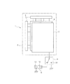
図1は、本実施形態の表示装置の外観を示す斜視図であり、図2は、本実施形態の表示装置の内部構成を示すブロック図である。この図1に示すように、表示装置1は、電気泳動表示体2、TFT(Thin Film Transistor)駆動回路3、接続先切り替えスイッチ4及び外部電源用コネクタ5を含んで構成される。
Hereinafter, an embodiment of a display device of the present invention will be described with reference to the drawings.
<Configuration of display device>
FIG. 1 is a perspective view showing the appearance of the display device of this embodiment, and FIG. 2 is a block diagram showing the internal configuration of the display device of this embodiment. As shown in FIG. 1, the display device 1 includes an
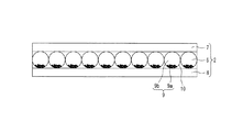
この電気泳動表示体2は、表示装置1の前面中央に配置され、表示層6及び一対の電極7、8を含んで構成される。
これらのうち、表示層6は、図1のA−A線で電気泳動表示体2を破断した図3に示すように、負に帯電された黒色の帯電粒子9aと、白色の分散媒9bとで形成される電気泳動分散液9を内包する複数のマイクロカプセル10が配された層である。
The
Among these, the
また、一対の電極7、8は、表示層6を挟み込むように配置され、前面側を覆う透明電極7と、背面側を覆う非透明電極8とで形成される。また、透明電極7は、共通電極を形成し、接続先切り替えスイッチ4によって、アース端子11に接続されたり、外部電源用コネクタ5のコネクタ電源端子12(後述)に接続されたりする。さらに、非透明電極8は、マトリクス状に配置された複数の画素電極を形成し、TFT駆動回路3によって、各画素電極それぞれが任意の電位とされる。
The pair of
さらに、TFT駆動回路3は、非透明電極8に形成された複数の画素電極それぞれが、表示させる情報に応じた電位となるように、各画素電極のTFTを駆動する。
また、接続先切り替えスイッチ4は、表示装置1の下端右側に配置され、左右にスライド操作可能なスライドスイッチで形成される。そして、接続切り替えスイッチ4は、右側にスライド操作されると、電気泳動表示体2の透明電極7をアース端子11に接続し、左側にスライド操作されると、外部電源用コネクタ5のコネクタ電源端子12(後述)に接続する。なお、接続先切り替えスイッチ4は、情報を表示させているときに、誤ってスライド操作されることがないように、筐体外側の凹部内にスライドバーが設けられている。
Furthermore, the
In addition, the connection
さらに、外部電源用コネクタ5は、表示装置1の下端左側に配置され、凹状のコネクタ電源端子12とコネクタアース端子13とが左右に形成される。そして、外部電源用コネクタ5のコネクタ電源端子12及びコネクタアース端子13は、図4に示すように、外部電源供給用プラグ14の凸状のプラグ電源端子15及びプラグアース端子16を同時に差し込み可能となっている。ここで、外部電源供給用プラグ14は、表示装置1とは別体に設けられ、コネクタ電源端子12から常時+15Vの電位を供給するプラグである。
<表示装置の動作>
次に、本実施形態の表示装置1の動作を具体的状況に基づいて説明する。
Further, the external
<Operation of display device>
Next, the operation of the display device 1 of the present embodiment will be described based on a specific situation.
まず、情報を表示させるときには、接続切り替えスイッチ4を右側にスライド操作し、電気泳動表示体2の透明電極7をアース端子11に接続させた後、TFT駆動回路3に、各画素電極のTFTを駆動させる。すると、透明電極7と非透明電極8との間に所定の電圧が印可され、それらの電極7、8に挟まれた任意のマイクロカプセル10の帯電粒子9aが透明電極7側に吸着され、その吸着された帯電粒子9aによって、透明電極7側、つまり電気泳動表示体2の前面側に任意の情報が表示される。
First, when displaying information, the
また、会社の秘密情報を表示させていたときに、表示装置1を落としてしまい、TFT駆動回路3が破損したとする。そして、TFT駆動回路3が動作しなくなり、非透明電極8の電位が「0」、つまり、接地電位となり、TFT駆動回路3によって表示を消すことができなくなってしまったとする。そのようなときには、接続先切り替えスイッチ4を左側にスライド操作し、電気泳動表示体2の透明電極7を外部電源用コネクタ5のコネクタ電源端子12に接続させた後、外部電源供給用プラグ14を外部電源用コネクタ5に差し込む。すると、電気泳動表示体2の透明電極7が外部電源供給用プラグ14のプラグ電源端子15と電気的に接続され、透明電極7の電位が+15Vとなり、透明電極7の電位が非透明電極8の電位より大きくなる。そして、それらの電極7、8に挟まれたマイクロカプセル10の帯電粒子9aが非透明電極8側に全て吸着され、その吸着によって、透明電極7側、つまり電気泳動表示体の前面側の全体に分散媒9bの色(白色)が表示とされ、表示されていた秘密情報が消去される。
Further, it is assumed that the display device 1 is dropped when the company secret information is displayed, and the
このように、本実施形態の表示装置1によれば、TFT駆動回路3によらず、一対の電極7、8間に電圧を印可することができる。そのため、他人に見られては困る情報を表示させていたときに、装置が故障し、TFT駆動回路3が動作しなくなった場合にも、表示層6に電圧を印加することができ、表示されている情報を消去させることができる。
ちなみに、TFT駆動回路3にのみ、一対の電極7、8間に電圧を印可させるようにした方法によれば、TFT駆動回路3が動作しなくなったときに、他人に見られては困る情報を表示させていた場合には、表示装置1を修理に出すこともできず、また、そのまま廃棄してしまうこともできない。そのため、表示させていた情報が見られることがないように、表示層6を破壊しなければならず、多くの費用や手間がかかってしまう。
Thus, according to the display device 1 of the present embodiment, a voltage can be applied between the pair of
By the way, according to the method in which only the
なお、本実施形態では、接続先切り替えスイッチ4を左右にスライド操作可能なスライドスイッチで形成する例を示したが、これに限られるものではなく、例えば、外部電源用コネクタ5に外部電源供給用プラグ14が差し込まれたことを検出するセンサで形成するようにしてもよい。そして、外部電源供給用プラグ14が差し込まれたことが検出された場合には、外部電源用コネクタ5のコネクタ電源端子12に接続し、差し込まれたことが検出されていない場合には、電気泳動表示体2の透明電極7をアース端子11に接続するようにしてもよい。そのようにすれば、透明電極7の接続先を切り替える手間を省くことができ、また、情報を表示させているときに、接続先が誤って切り替えられてしまうことが防止される。
In this embodiment, the connection
以上、図2及び図5の表示層6が特許請求の範囲の欄に記載の表示層を構成し、以下同様に、図2及び図5の透明電極7及び非透明電極8が電極を構成し、図1〜図3及び図5の電気泳動表示体2が記憶性表示体2を構成し、図2及び図5のTFT駆動回路3が駆動回路を構成し、図2及び図5の接続先切り替えスイッチ4及び外部電源用コネクタ5が情報消去用回路を構成し、図3のマイクロカプセル10が封入領域を構成する。
As described above, the
また、本発明の表示装置及び情報消去方法は、上記実施の形態の内容に限定されるものではなく、本発明の趣旨を逸脱しない範囲で適宜変更可能である。
例えば、上記実施形態では、透明電極7の接続先をアース端子11と外部電源用コネクタ5のコネクタ電源端子12とのいずれかに切り替え可能とした例を示したが、これに限られるものではない。例えば、透明電極7の接続先を外部電源用コネクタ5のコネクタ電源端子12に代えて、自装置の駆動用電源17の電源端子18に切り替え可能としてもよい。具体的には、図5に示すように、接続切り替えスイッチ4を、右側にスライド操作されると、電気泳動表示体2の透明電極7をアース端子11に接続し、左側にスライド操作されると、自装置の駆動用電源17の電源端子18に接続するように構成する。なお、自装置の駆動用電源17は、情報を表示させるときに、TFT駆動回路3等といった、各回路を駆動するための電源である。
Further, the display device and the information erasing method of the present invention are not limited to the contents of the above embodiment, and can be appropriately changed without departing from the gist of the present invention.
For example, in the above-described embodiment, the example in which the connection destination of the
また、電気泳動表示体2に情報を表示させる例を示したが、これに限られるものではなく、例えば、白黒塗り分けたビーズを帯電させ、電気をかけ回転させることで白黒の表示を可能とする表示体に表示させるようにしてもよい。
In addition, although an example in which information is displayed on the
1は表示装置、2は電気泳動表示体、3はTFT駆動回路、4は接続先切り替えスイッチ、5は外部電源用コネクタ、6は表示層、7は透明電極、8は非透明電極、9aは帯電粒子、9bは分散媒、9は電気泳動分散液、10はマイクロカプセル、11はアース端子、12はコネクタ電源端子、13はコネクタアース端子、14は外部電源供給用プラグ、15はプラグ電源端子、16はプラグアース端子、17は駆動用電源、18は電源端子 1 is a display device, 2 is an electrophoretic display, 3 is a TFT drive circuit, 4 is a connection destination switch, 5 is an external power connector, 6 is a display layer, 7 is a transparent electrode, 8 is a non-transparent electrode, and 9a is Charged particles, 9b dispersion medium, 9 electrophoretic dispersion liquid, 10 microcapsule, 11 ground terminal, 12 connector power terminal, 13 connector ground terminal, 14 external power supply plug, 15 plug power terminal , 16 is a plug ground terminal, 17 is a drive power supply, and 18 is a power supply terminal.
Claims (7)
前記表示層に所定の画像が表示されるように、前記画素電極の電位を制御して、前記複数の画素電極及び前記共通電極間に所定の電圧を印加する駆動回路と、
前記駆動回路と独立して、前記共通電極にのみ所定電源を接続することで、前記画素電極及び前記共通電極の間に電位差を生じさせる情報消去用回路と、を備えたことを特徴とする表示装置。 A display layer capable of displaying an image by displaying a predetermined color according to an applied voltage, a memory display body including a plurality of pixel electrodes and a common electrode disposed so as to sandwich the display layer ;
A drive circuit for controlling a potential of the pixel electrode so that a predetermined image is displayed on the display layer and applying a predetermined voltage between the plurality of pixel electrodes and the common electrode ;
Independently of the driving circuit, the common electrode only by connecting a predetermined power supply, display, characterized in that and an information erasing circuit generating a potential difference between the pixel electrode and the common electrode apparatus.
前記情報消去用回路の接続を、基準電位を供給する端子と前記外部電源の電源端子とのいずれかの接続に切り替え可能な切り替え手段を備えたことを特徴とする請求項1に記載の表示装置。 The predetermined power source is an external power source,
2. The display device according to claim 1, further comprising switching means capable of switching the connection of the information erasing circuit to a connection between a terminal for supplying a reference potential and a power supply terminal of the external power source. .
前記情報消去用回路の接続を、基準電位を供給する端子と前記駆動用電源の電源端子とのいずれかの接続に切り替え可能な切り替え手段を備えたことを特徴とする請求項1に記載の表示装置。 The predetermined power source is a driving power source included in the device itself,
The display according to claim 1, further comprising switching means capable of switching the connection of the information erasing circuit to a connection between a terminal for supplying a reference potential and a power supply terminal of the driving power supply. apparatus.
前記表示層に前記所定の画像が表示されているときに、前記駆動回路が動作しなくなった場合、前記駆動回路と独立して動作可能に設けられた情報消去用回路により、前記共通電極にのみ所定電源を接続し、前記画素電極及び前記共通電極の間に電位差を生じさせることで、前記表示層に表示されている前記所定の画像を消去することを特徴とする表示装置の情報消去方法。 A display layer capable of displaying an image by displaying a predetermined color in accordance with an applied voltage, a memory display body including a plurality of pixel electrodes and a common electrode arranged so as to sandwich the display layer, and a predetermined display on the display layer as images are displayed by controlling the potential of the pixel electrode, and a driving circuit for applying a predetermined voltage between the plurality of pixel electrodes and the common electrode, the display layer from the display device provided with An information erasing method of a display device for erasing the predetermined image being displayed,
Wherein when the display layer wherein the predetermined image is displayed, if the drive circuit becomes rather operates, by the driving circuit and independent to operatively provided information erasing circuit, wherein only the common electrode connecting the predetermined power, the by generating a potential difference between the pixel electrode and the common electrode, the display device characterized by erasing the predetermined image displayed on the display layer How to erase information.
Priority Applications (6)
| Application Number | Priority Date | Filing Date | Title |
|---|---|---|---|
| JP2004065630A JP4151591B2 (en) | 2004-03-09 | 2004-03-09 | Display device and display device information erasing method |
| PCT/JP2005/003613 WO2005086132A1 (en) | 2004-03-09 | 2005-03-03 | Display device and image blanking method |
| CNA2005800002167A CN1771528A (en) | 2004-03-09 | 2005-03-03 | Display device and image erasing method |
| KR1020057022284A KR100746802B1 (en) | 2004-03-09 | 2005-03-03 | Display device and image blanking method |
| US11/074,328 US7733324B2 (en) | 2004-03-09 | 2005-03-04 | Display device and image erasing method |
| US12/621,734 US8797257B2 (en) | 2004-03-09 | 2009-11-19 | Display device having an image erasing circuit that is independent of the driving circuit and an image erasing method |
Applications Claiming Priority (1)
| Application Number | Priority Date | Filing Date | Title |
|---|---|---|---|
| JP2004065630A JP4151591B2 (en) | 2004-03-09 | 2004-03-09 | Display device and display device information erasing method |
Publications (3)
| Publication Number | Publication Date |
|---|---|
| JP2005257755A JP2005257755A (en) | 2005-09-22 |
| JP2005257755A5 JP2005257755A5 (en) | 2007-06-28 |
| JP4151591B2 true JP4151591B2 (en) | 2008-09-17 |
Family
ID=34918263
Family Applications (1)
| Application Number | Title | Priority Date | Filing Date |
|---|---|---|---|
| JP2004065630A Expired - Fee Related JP4151591B2 (en) | 2004-03-09 | 2004-03-09 | Display device and display device information erasing method |
Country Status (5)
| Country | Link |
|---|---|
| US (2) | US7733324B2 (en) |
| JP (1) | JP4151591B2 (en) |
| KR (1) | KR100746802B1 (en) |
| CN (1) | CN1771528A (en) |
| WO (1) | WO2005086132A1 (en) |
Families Citing this family (9)
| Publication number | Priority date | Publication date | Assignee | Title |
|---|---|---|---|---|
| JP4561111B2 (en) * | 2004-01-30 | 2010-10-13 | セイコーエプソン株式会社 | Display device |
| JP2006276627A (en) * | 2005-03-30 | 2006-10-12 | Seiko Epson Corp | Information display device and electrode driving circuit |
| JP5790968B2 (en) * | 2008-08-18 | 2015-10-07 | Nltテクノロジー株式会社 | Display device and manufacturing method thereof |
| JP5296177B2 (en) * | 2011-10-28 | 2013-09-25 | 株式会社東芝 | Electronics |
| DE102013226167A1 (en) * | 2013-12-17 | 2015-06-18 | Lemförder Electronic GmbH | Method and apparatus for placing an electronic display device in a safe state and control device for controlling an electronic display device |
| US9411374B2 (en) * | 2014-02-20 | 2016-08-09 | Amazon Technologies, Inc. | Electronic device display stack |
| US10565942B2 (en) | 2014-07-29 | 2020-02-18 | Hewlett-Packard Development Company, L.P. | Display device |
| JP2018097005A (en) * | 2015-03-20 | 2018-06-21 | 日本電気株式会社 | Display unit, display system, display control method, and program |
| CN112327528B (en) * | 2019-08-05 | 2023-04-28 | 深圳市芯卓微科技有限公司 | Circularly alternating unipolar pulse LCD liquid crystal screen image erasing circuit and method |
Family Cites Families (13)
| Publication number | Priority date | Publication date | Assignee | Title |
|---|---|---|---|---|
| JPH01195783A (en) * | 1988-01-29 | 1989-08-07 | Victor Co Of Japan Ltd | Picture display device |
| JPH11271707A (en) | 1998-03-19 | 1999-10-08 | Toshiba Corp | Liquid crystal display device |
| JP3717097B2 (en) * | 1998-07-29 | 2005-11-16 | 富士通株式会社 | Ferroelectric memory |
| US6762744B2 (en) * | 2000-06-22 | 2004-07-13 | Seiko Epson Corporation | Method and circuit for driving electrophoretic display, electrophoretic display and electronic device using same |
| JP2003050565A (en) * | 2000-06-29 | 2003-02-21 | Matsushita Electric Ind Co Ltd | Liquid crystal display system, display signal supply device, and liquid crystal display device |
| JP2002014379A (en) * | 2000-06-30 | 2002-01-18 | Tdk Corp | Electrophoresis display device |
| JP2002075064A (en) * | 2000-08-23 | 2002-03-15 | Tdk Corp | Anisotropic conductive film and its manufacturing method, and display using anisotropic conductive film |
| JP3719172B2 (en) | 2000-08-31 | 2005-11-24 | セイコーエプソン株式会社 | Display device and electronic device |
| US6900789B2 (en) * | 2000-11-16 | 2005-05-31 | Minolta Co., Ltd. | Reversible image display medium |
| JP4885353B2 (en) * | 2000-12-28 | 2012-02-29 | ティーピーオー ホンコン ホールディング リミテッド | Liquid crystal display |
| JP2002357853A (en) | 2001-03-30 | 2002-12-13 | Seiko Epson Corp | Elctrophoresis device, driving method for the same device and electronic equipment |
| JP2003195831A (en) | 2001-12-27 | 2003-07-09 | Matsushita Electric Ind Co Ltd | Liquid crystal display device |
| JP3922984B2 (en) | 2002-08-06 | 2007-05-30 | 松下電器産業株式会社 | Nonvolatile display device |
-
2004
- 2004-03-09 JP JP2004065630A patent/JP4151591B2/en not_active Expired - Fee Related
-
2005
- 2005-03-03 KR KR1020057022284A patent/KR100746802B1/en not_active IP Right Cessation
- 2005-03-03 CN CNA2005800002167A patent/CN1771528A/en active Pending
- 2005-03-03 WO PCT/JP2005/003613 patent/WO2005086132A1/en active Application Filing
- 2005-03-04 US US11/074,328 patent/US7733324B2/en active Active - Reinstated
-
2009
- 2009-11-19 US US12/621,734 patent/US8797257B2/en not_active Expired - Fee Related
Also Published As
| Publication number | Publication date |
|---|---|
| US20100066717A1 (en) | 2010-03-18 |
| WO2005086132A1 (en) | 2005-09-15 |
| US20050206813A1 (en) | 2005-09-22 |
| CN1771528A (en) | 2006-05-10 |
| JP2005257755A (en) | 2005-09-22 |
| US8797257B2 (en) | 2014-08-05 |
| US7733324B2 (en) | 2010-06-08 |
| KR20060036386A (en) | 2006-04-28 |
| KR100746802B1 (en) | 2007-08-06 |
Similar Documents
| Publication | Publication Date | Title |
|---|---|---|
| US8797257B2 (en) | Display device having an image erasing circuit that is independent of the driving circuit and an image erasing method | |
| HK1093811A1 (en) | Methods for controlling electro-optic displays | |
| US6636194B2 (en) | Electrooptic device and electronic equipment | |
| JP2004029703A5 (en) | ||
| KR101838047B1 (en) | Electrophoresis display device and driving method the same | |
| JP5583328B2 (en) | Display device | |
| JP2009069411A (en) | Electrophoretic display device, controller, applying method, program, and applying device | |
| TW200508766A (en) | Display device | |
| JP2005257755A5 (en) | ||
| CN103137078A (en) | Display device and method for controlling display device | |
| JP2659858B2 (en) | LCD drive | |
| JPH1048673A (en) | Electrophoretic recording medium and electrophoretic display device | |
| JP2008170527A (en) | Display device and voltage application circuit | |
| JP5478395B2 (en) | Electrophoretic display device and driving method thereof | |
| JP4649890B2 (en) | Driving device for image display medium | |
| JP2000148116A (en) | Display device | |
| JP2001311931A (en) | Electronic paper, electronic paper file and electronic pen | |
| JP5081074B2 (en) | Display eraser | |
| JP2004317648A (en) | Display data erasing/writing device and picture display method using the device | |
| CN115578982B (en) | Display driving circuit, electronic paper and refreshing driving method thereof | |
| JP5780079B2 (en) | Electronic paper information terminal | |
| JP3856027B2 (en) | Electro-optical device and electronic apparatus | |
| JP5145122B2 (en) | Display control device | |
| JP2002196371A (en) | Picture erasing device, picture display medium, picture forming system and picture erasing method | |
| JP2006276627A (en) | Information display device and electrode driving circuit |
Legal Events
| Date | Code | Title | Description |
|---|---|---|---|
| A521 | Written amendment |
Free format text: JAPANESE INTERMEDIATE CODE: A523 Effective date: 20070309 |
|
| A621 | Written request for application examination |
Free format text: JAPANESE INTERMEDIATE CODE: A621 Effective date: 20070309 |
|
| A131 | Notification of reasons for refusal |
Free format text: JAPANESE INTERMEDIATE CODE: A131 Effective date: 20071127 |
|
| A521 | Written amendment |
Free format text: JAPANESE INTERMEDIATE CODE: A523 Effective date: 20080124 |
|
| A131 | Notification of reasons for refusal |
Free format text: JAPANESE INTERMEDIATE CODE: A131 Effective date: 20080219 |
|
| TRDD | Decision of grant or rejection written | ||
| A01 | Written decision to grant a patent or to grant a registration (utility model) |
Free format text: JAPANESE INTERMEDIATE CODE: A01 Effective date: 20080610 |
|
| A01 | Written decision to grant a patent or to grant a registration (utility model) |
Free format text: JAPANESE INTERMEDIATE CODE: A01 |
|
| A61 | First payment of annual fees (during grant procedure) |
Free format text: JAPANESE INTERMEDIATE CODE: A61 Effective date: 20080623 |
|
| R150 | Certificate of patent or registration of utility model |
Free format text: JAPANESE INTERMEDIATE CODE: R150 |
|
| FPAY | Renewal fee payment (event date is renewal date of database) |
Free format text: PAYMENT UNTIL: 20110711 Year of fee payment: 3 |
|
| FPAY | Renewal fee payment (event date is renewal date of database) |
Free format text: PAYMENT UNTIL: 20110711 Year of fee payment: 3 |
|
| FPAY | Renewal fee payment (event date is renewal date of database) |
Free format text: PAYMENT UNTIL: 20120711 Year of fee payment: 4 |
|
| FPAY | Renewal fee payment (event date is renewal date of database) |
Free format text: PAYMENT UNTIL: 20120711 Year of fee payment: 4 |
|
| FPAY | Renewal fee payment (event date is renewal date of database) |
Free format text: PAYMENT UNTIL: 20130711 Year of fee payment: 5 |
|
| LAPS | Cancellation because of no payment of annual fees |