EP1184685A2 - Optical element having anti-reflection film - Google Patents
Optical element having anti-reflection film Download PDFInfo
- Publication number
- EP1184685A2 EP1184685A2 EP01120616A EP01120616A EP1184685A2 EP 1184685 A2 EP1184685 A2 EP 1184685A2 EP 01120616 A EP01120616 A EP 01120616A EP 01120616 A EP01120616 A EP 01120616A EP 1184685 A2 EP1184685 A2 EP 1184685A2
- Authority
- EP
- European Patent Office
- Prior art keywords
- layer
- refractive index
- antireflection film
- layers
- film
- Prior art date
- Legal status (The legal status is an assumption and is not a legal conclusion. Google has not performed a legal analysis and makes no representation as to the accuracy of the status listed.)
- Granted
Links
Classifications
-
- G—PHYSICS
- G02—OPTICS
- G02B—OPTICAL ELEMENTS, SYSTEMS OR APPARATUS
- G02B1/00—Optical elements characterised by the material of which they are made; Optical coatings for optical elements
- G02B1/10—Optical coatings produced by application to, or surface treatment of, optical elements
-
- G—PHYSICS
- G02—OPTICS
- G02B—OPTICAL ELEMENTS, SYSTEMS OR APPARATUS
- G02B1/00—Optical elements characterised by the material of which they are made; Optical coatings for optical elements
- G02B1/10—Optical coatings produced by application to, or surface treatment of, optical elements
- G02B1/11—Anti-reflection coatings
- G02B1/113—Anti-reflection coatings using inorganic layer materials only
- G02B1/115—Multilayers
Definitions
- the present invention relates to an optical element having an antireflection film a plastic substrate, in particular, to an optical element having an antireflection film on a plastic substrate, which has good heat resistance.
- Japanese Patent Laid-Open No. 291501/1990 discloses an optical element formed with an antireflection film, which has a high-refraction layer of ⁇ /2 containing titanium dioxide as a major component.
- the object of this invention is to provide an optical element having an antireflection film on a plastic substrate and having good heat resistance.
- the present inventors have assiduously studied to solve the problems noted above, and, as a result, have found that the heat resistance of the optical element is significantly improved by novel means of an equivalent film of at least three layers, while utilizing a high-reflection layer and a layer made of a low-refraction substance, silicon dioxide.
- An equivalent film is a film comprising more than one layer derived from different stable materials.
- optical properties e.g. refractive index
- the high-refraction layer of ⁇ /2 is a three-layered equivalent film, the optical element having good heat resistance and antireflection property is obtained.
- the high-reflection layer of ⁇ /2 may be made of an equivalent film of more than three layers.
- the odd-numbered layer of the equivalent film of ⁇ /2 is preferably a layer containing a known high-refraction vapor-depositing substance such as titanium oxide, zirconium oxide, tantalum oxide and niobium oxide, more preferably a layer made of at least one vapor-depositing substance selected from TiO 2 , Ta 2 O 5 and Nb 2 O 5 , and most preferably a layer of Nb 2 O 5 as the vapor-depositing substance.
- a known high-refraction vapor-depositing substance such as titanium oxide, zirconium oxide, tantalum oxide and niobium oxide
- a layer made of at least one vapor-depositing substance selected from TiO 2 , Ta 2 O 5 and Nb 2 O 5 and most preferably a layer of Nb 2 O 5 as the vapor-depositing substance.
- the resultant refractive index of the high-refraction layer of ⁇ /2 is in the range of from 1.80 to 2.40, but preferably in the range of from 1.85 to 2.25 for better physical properties.
- the film constitution of the high-refraction layer of ⁇ /2 is so made that it satisfies the defined range of the refractive index.
- the layer of ⁇ /4 to be formed on the high-refraction layer of ⁇ /2 is preferably a silicon dioxide layer.
- the layer of ⁇ /4 to be formed under the high-refraction layer of ⁇ /2 is preferably an equivalent film of at least two layers for good antireflection property and heat resistance.
- the film is preferably constructed of a two-layered equivalent film made of a silicon dioxide layer and a layer of a high-refraction vapor-depositing substance such as titanium oxide, zirconium oxide, tantalum oxide and niobium oxide, or a two-layered equivalent film made of a silicon dioxide layer and a niobium oxide layer.
- the raw materials for vapor deposition in forming the equivalent film of ⁇ /4 are the same as those for vapor deposition in forming the equivalent film of ⁇ /2.
- niobium oxide layer For forming the preferred niobium oxide layer, a method using 100 % niobium oxide for the vapor-depositing substance to form the layer according to an ion-assisted process , or a method of sintering a powder containing niobium oxide, zirconium oxide and yttrium oxide and optionally containing aluminum oxide, generating a vapor of the oxide mixture from the sintered material, and depositing the vapor on a substrate are preferably employed.
- a blend ratio of the material to be sintered is preferably such that niobium oxide accounts for from 60 to 90 % by weight of the whole of the composition for vapor deposition, zirconium oxide for from 5 to 20 % by weight, and yttrium oxide for from 5 to 35 % by weight, for ensuring good physical properties of the film.
- niobium oxide accounts for from 60 to 90 % by weight of the whole of the composition for vapor deposition, zirconium oxide for from 5 to 20 % by weight, and yttrium oxide for from 5 to 35 % by weight, for ensuring good physical properties of the film.
- aluminum oxide is added, its amount is preferably from 0.3 to 7.5 % by weight of the total of zirconium oxide and yttrium oxide therein.
- the optical element of the invention has a basic layer provided between the plastic substrate and the antireflection film.
- Silicon dioxide or metallic niobium is preferred for the basic layer, and metallic niobium is more preferred.
- its film thickness is preferably from 0.1 ⁇ to 5 ⁇ in view of the film strength; and in case of metallic niobium, its film thickness is preferably from 0.005 ⁇ to 0.015 ⁇ , for ensuring the film transparency.
- the advantages of the preferred basic layer of metallic niobium are that it ensures good adhesiveness between the plastic substrate and the antireflection film, it is excellent in heat resistance, impact resistance and abrasion resistance, and its absorption intrinsic to metal is low.
- the metallic niobium (Nb) layer is formed in an ion-assisted process.
- argon (Ar) is preferred for the ionizing gas for preventing oxidation of the film being formed. This stabilizes the quality of the film formed and enables easy control of the thickness of the film by the use of an optical film thickness meter.
- the plastic substrate may be subjected to ion gun pretreatment before the basic layer is formed thereon.
- the ionizing gas in the ion gun pretreatment may be any of oxygen or Ar.
- the accelerating voltage is from 50 V to 200 V, and the accelerating current is from 50 mA to 150 mA.
- An ordinary vapor deposition process, an ion-assisted process or the like is employable for forming the antireflection film in the optical element of the invention.
- the plastic substrate used for the optical substrate of the invention is not specifically defined, including, for example, methyl methacrylate homopolymers, copolymers of methyl methacrylate and one or more other monomers, diethylene glycol bisallyl carbonate homopolymers, copolymers of diethylene glycol bisallyl carbonate and one or more other monomers, sulfur-containing copolymers, halogen-containing copolymers, polycarbonates, polystyrenes, polyvinyl chlorides, unsaturated polyesters, polyethylene terephthalates, and polyurethanes.
- the optical element of the invention may have a cured film between the plastic substrate and the basic layer.
- cured film For the cured film, generally used is one made by curing a coating composition that comprises metal oxide colloid particles and an organosilicon compound.
- the metal oxide colloid particles may be, for example, colloid particles of tungsten oxide (WO 3 ), zinc oxide (ZnO), silicon oxide (SiO 2 ), aluminum oxide (Al 2 O 3 ), titanium oxide (TiO 2 ), zirconium oxide (ZrO 2 ), tin oxide (SnO 2 ), beryllium oxide (BeO) or antimony oxide (Sb 2 O 5 ).
- tungsten oxide WO 3
- ZnO zinc oxide
- silicon oxide SiO 2
- Al 2 O 3 aluminum oxide
- TiO 2 titanium oxide
- ZrO 2 zirconium oxide
- tin oxide SnO 2
- BeO beryllium oxide
- Sb 2 O 5 antimony oxide
- the invention further provides an optical element having an antireflection film which comprises a plastic substrate having a basic layer and an antireflection film of a ⁇ /4 - ⁇ /2 - ⁇ /4 type provided thereon, wherein the basic layer and the antireflection film are of a layer construction of 1st to 7th layers of basic layer (1st layer) and ⁇ 4 (2nd and 3rd layers) - ⁇ /2 (4th to 6th layers) - ⁇ /4 (7th layer), and which satisfies at least one of the requirements a) to j) set forth below:
- colloidal silica (Snowtex-40, available from Nissan Chemical Industries, Ltd.), 81.6 parts by weight of methyltrimethoxysilane and 176 parts by weight of ⁇ -glycidoxypropyltrimethoxysilane as organosilicon compounds, 2.0 parts by weight of 0.5 N hydrochloric acid, 20 parts by weight of acetic acid, and 90 parts by weight of water were charged into a glass container, and the solution was stirred at room temperature for 8 hours. Then, the resulting solution was left at room temperature for 16 hours to obtain a hydrolyzed solution.
- colloidal silica Snowtex-40, available from Nissan Chemical Industries, Ltd.
- 81.6 parts by weight of methyltrimethoxysilane and 176 parts by weight of ⁇ -glycidoxypropyltrimethoxysilane as organosilicon compounds 2.0 parts by weight of 0.5 N hydrochloric acid, 20 parts by weight of acetic acid, and 90 parts by weight of water were charged into a glass container, and the solution was stirred
- a plastic lens substrate (made from diethylene glycol bisallyl carbonate, and having a refractive index of 1.50, a center thickness of 2.0 mm and a power of lens of 0.00 - this may be hereinafter referred to as "substrate A"), which had been pretreated with an aqueous alkaline solution, was dipped in the coating solution. After completion of dipping, the plastic lens was taken out at a pulling rate of 20 cm/min. Then, the plastic lens was heated at 120°C for 2 hours to form a cured film.
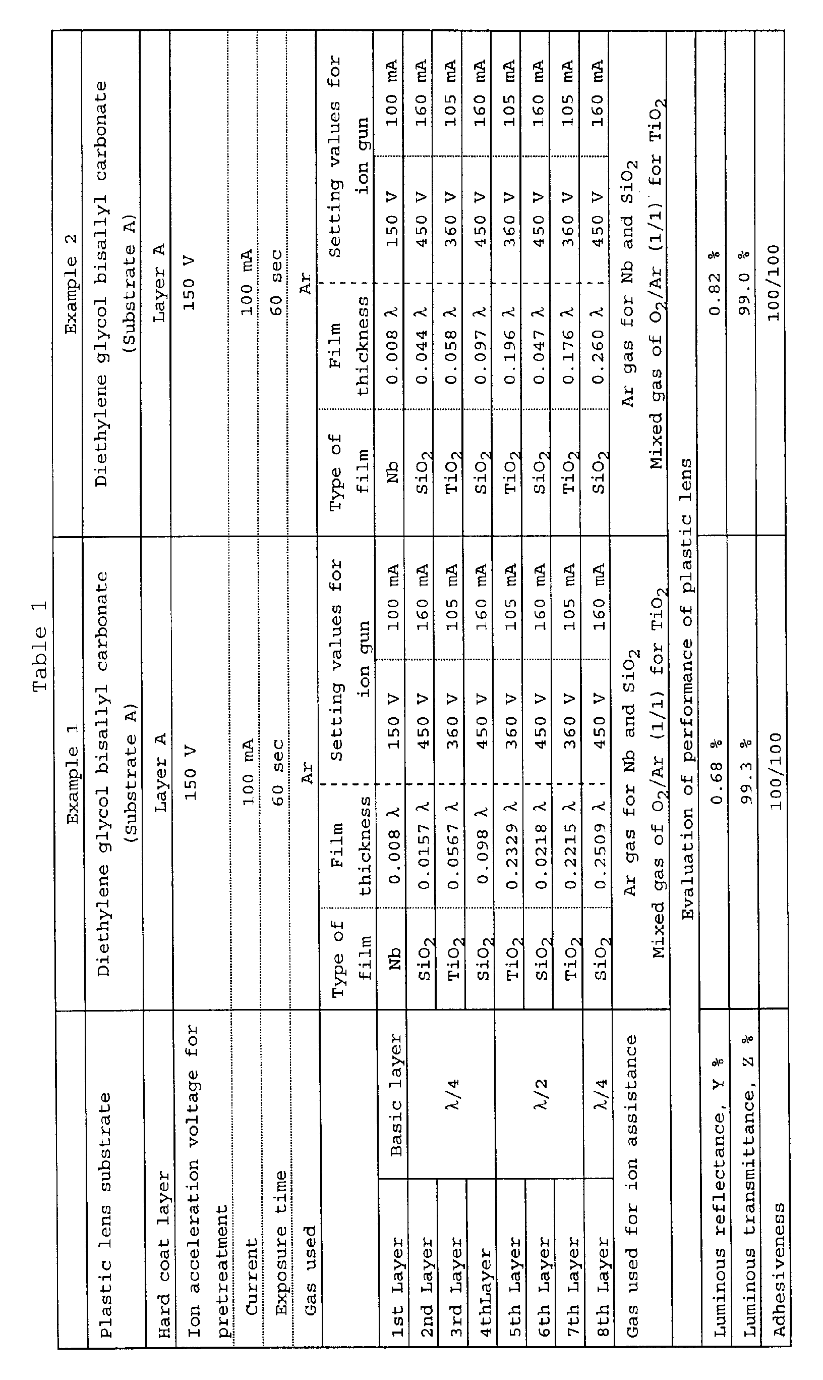
- the resulting plastic lens was subjected to an ion gun treatment according to an ion-assisted process using an Ar gas under the condition of the ion acceleration voltage and exposure time as shown in Tables 1 to 6, thereby making it have a cured hard coat layer (this is referred to as "layer A").
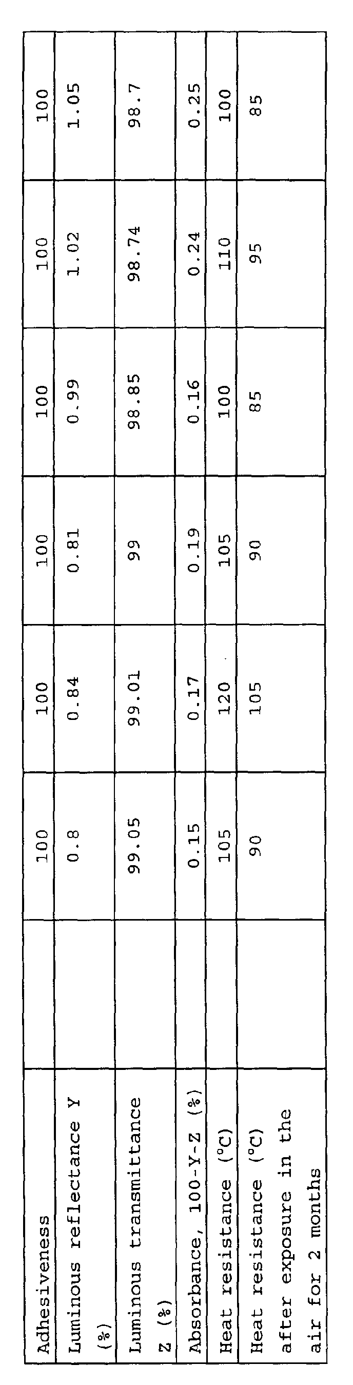
- the plastic lenses were evaluated according to the test methods (1) to (7) mentioned above, and the results are shown in Tables 1 to 6.
- the resultant refractive indices of ⁇ /4 and ⁇ /2 in Examples 1 to 6 are shown in Table 8.
- stannic oxide-zirconium oxide composite sol (dispersed in methanol, having a total metal oxide content of 31.5 % by weight and having a mean particle size of from 10 to 15 millimicrons), 300 parts by weight of ethyl cellosolve, 0.7 parts by weight of a lubricant, silicone surfactant, and 8 parts by weight of a curing agent, aluminum acetylacetonate. After well stirring, the mixture was filtered to prepare a coating solution.
- a plastic lens substrate (a plastic lens for eyeglass, EYAS (a trade name) made by Hoya Corporation, having a refractive index of at most 1.60 - this may be hereinafter referred to as "substrate B"), which had been pretreated with an aqueous alkaline solution, was dipped in the coating solution. After dipping, the plastic lens was taken out at a pulling rate of 20 cm/min. Then, the plastic lens was heated at 120°C for 2 hours to form a hard coat layer (the layer is referred to as "layer B").
- ⁇ -glycidoxypropyltrimethoxysilane 100 parts by weight of an organosilicon compound, ⁇ -glycidoxypropyltrimethoxysilane was charged into a glass container, to which were added 1.4 parts by weight of 0.01 N hydrochloric acid and 23 parts by weight of water with stirring. After the addition, the mixture was stirred for 24 hours to obtain a solution of hydrolyzed ⁇ -glycidoxypropyltrimethoxysilane.
- an inorganic particulate substance composite sol of particles composed mainly of titanium oxide, zirconium oxide and silicon oxide (dispersed in methanol, having a total solid content of 20 % by weight and having a mean particle size of from 5 to 15 millimicrons - in this, the atomic ratio of Ti/Si in the core fine particles is 10, and the ratio by weight of the shell to the core is 0.25) was mixed with 100 parts by weight of ethyl cellosolve, 0.5 parts by weight of a lubricant, silicone surfactant, and 3.0 parts by weight of a curing agent, aluminum acetylacetonate. The resulting mixture was added to the solution of hydrolyzed ⁇ -glycidoxypropyltrimethoxysilane, and well stirred. The mixture was filtered to prepare a coating solution.
- a plastic lens substrate (a plastic lens for eyeglass, TESLAID (a trade name) made by Hoya Corporation, having a refractive index of 1.71 - this may be hereinafter referred to as "substrate C"), which had been pretreated with an aqueous alkaline solution, was dipped in the coating solution. After completion of dipping, the plastic lens was taken out at a pulling rate of 20 cm/min. Then, the plastic lens was heated at 120°C for 2 hours to form a hard coat layer (the layer is referred to as "layer C").
- TESLAID a trade name
- Example 7 to 12 the composition A in the Tables was subjected to film formation not according to an ion-assisted process.
- the film made of the composition A in Examples 13 to 18, and the niobium oxide layer in Examples 19 to 24 were formed according to an ion-assisted process, in which the ratio of oxygen/argon was 9/1, and the ion gun condition was 320 A and 140 mA.
- the high-refraction substance used was titanium oxide, and its film was formed not according to an ion-assisted process.
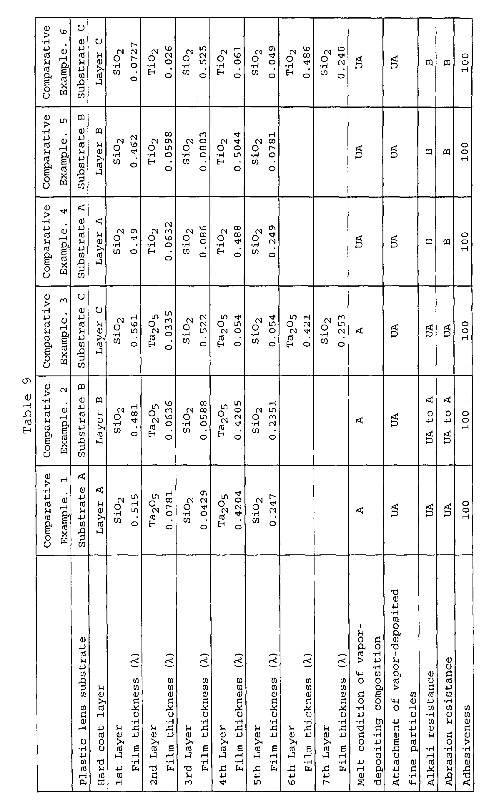
- tantalum oxide was used as the high-refraction vapor-depositing substance.
- a basic layer composed of silicon dioxide; a two-layered equivalent film of ⁇ /4 composed of a tantalum oxide layer and a silicon dioxide layer; a tantalum oxide layer of ⁇ /2; and a silicon dioxide layer of ⁇ /4 were formed.
- Comparative Example 3 the hard coat layer C, the substrate C, and tantalum oxide as the high-refraction vapor-depositing substance were used.
- Comparative Example 6 the hard coat layer C, the substrate C, and titanium oxide as the high-refraction vapor-depositing substance were used. In this, a 3rd layer composed of silicon dioxide; a two-layered equivalent film of ⁇ /4 composed of a titanium oxide layer and a silicon dioxide layer; a titanium oxide layer of ⁇ /2; and a silicon dioxide layer of ⁇ /4 were formed. In these Comparative Examples 1 to 6, the films were not formed according to an ion-assisted process.
- Comparative Examples 1, 2 and 3 were inferior in the heat resistance to Examples 22, 23 and 24, respectively.
- Example 25 Example 26
- Example 27 Plastic lens substrate Substrate A Substrate B Substrate C Hard coat layer Layer A Layer B Layer C 1st Layer Film thickness ( ⁇ ) Basic layer SiO 2 0.51 SiO 2 0.421 SiO 2 0.079 2nd Layer Film thickness ( ⁇ ) ⁇ /4 TiO 2 0.0435 TiO 2 0.0224 TiO 2 0.275 3rd Layer Film thickness ( ⁇ ) SiO 2 0.1089 SiO 2 0.0972 SiO 2 0.5761 4th Layer Film thickness ( ⁇ ) ⁇ /2 TiO 2 0.1468 TiO 2 0.1327 TiO 2 0.135 5th Layer Film thickness ( ⁇ ) SiO 2 0.0689 SiO 2 0.0768 SiO 2 0.102 6th Layer Film thickness ( ⁇ ) TiO 2 0.1474 TiO 2 0.1665 TiO 2 0.143 7th Layer Film thickness ( ⁇ ) ⁇ /4 SiO 2 0.2716 SiO 2 0.291 SiO 2 0.2954 Melt condition of
- the optical element having an antireflection film of the invention has the advantages of good luminous reflectance, luminous transmittance, adhesiveness, abrasion resistance, alkali resistance and impact resistance, and has the additional advantage of improved heat resistance.
- the odd-numbered layer of the equivalent film of ⁇ /2 is a layer of at least one metal oxide selected from titanium oxide, zirconium oxide, niobium oxide and tantalum oxide, more preferably niobium oxide.
- the antireflection film as well as the optical element having an antireflection film of the invention may be used for eyeglasses.
Landscapes
- Physics & Mathematics (AREA)
- General Physics & Mathematics (AREA)
- Optics & Photonics (AREA)
- Chemical & Material Sciences (AREA)
- Inorganic Chemistry (AREA)
- Surface Treatment Of Optical Elements (AREA)
- Laminated Bodies (AREA)
Abstract
Description
the basic layer and the antireflection film are of a layer construction of 1st to 7th layers of basic layer (1st layer) and λ4 (2nd and 3rd layers) - λ/2 (4th to 6th layers) - λ/4 (7th layer), and which satisfies at least one of the requirements a) to j) set forth below:
| Constitution (a) | |||
| Plastic substrate | Range of refractive index | ||
| 1st Layer (SiO2 layer) | Basic layer | 1.43 to 1.47 | |
| 2nd Layer (high-refraction layer) | λ/4 | 2.04 to 2.37 | Resultant refractive index 1.65 to 1.80 |
| 3rd Layer (SiO2 layer) | 1.43 to 1.47 | ||
| 4th Layer (high-refraction layer) | λ/2 | 2.04 to 2.37 | Resultant refractive index 1.85 to 2.25 |
| 5th Layer (SiO2 layer) | 1.43 to 1.47 | ||
| 6th Layer (high-refraction layer) | 2.04 to 2.37 | ||
| 7th Layer (SiO2 layer) | λ/4 | 1.40 to 1.47 | |
| Constitution (b) | |||
| Plastic substrate | Range of refractive index | ||
| 1st Layer (SiO2 layer) | Basic layer | 1.43 to 1.47 | |
| 2nd Layer (high-refraction layer) | λ/4 | 2.04 to 2.37 | Resultant refractive index 1.65 to 1.80 |
| 3rd Layer (SiO2 layer) | 1.43 to 1.47 | ||
| 4th Layer (high-refraction layer) | λ/2 | 2.04 to 2.37 | Resultant refractive index 1.85 to 2.25 |
| 5th Layer (SiO2 layer) | 1.43 to 1.47 | ||
| 6th Layer (high-refraction layer) | 2.04 to 2.37 | ||
| 7th Layer (SiO2 layer) | 1.43 to 1.47 | ||
| 8th Layer (high-refraction layer) | 2.04 to 2.37 | ||
| 9th Layer (SiO2 layer) | λ/4 | 1.43 to 1.47 | |
| Constitution (c) | |||
| Plastic substrate | Range of Refractive Index | ||
| 1st Layer (metallic niobium layer) | Basic layer Film thickness: 0.005 λ to 0.015 λ | 1.40 to 1.47 | |
| 2nd Layer (SiO2 layer) | λ/4 | 1.43 to 1.47 | Resultant refractive index 1.65 to 1.80 |
| 3rd Layer (high-refraction layer) | 2.04 to 2.37 | ||
| 4th Layer (SiO2 layer) | 1.43 to 1.47 | ||
| 5th Layer (high-refraction layer) | λ/2 | 2.04 to 2.37 | Resultant refractive index 1.85 to 2.25 |
| 6th Layer (SiO2 layer) | 1.43 to 1.47 | ||
| 7th Layer (high-refraction layer) | 2.04 to 2.37 | ||
| 8th Layer (SiO2 layer) | λ/4 | 1.43 to 1.47 |
- UA:
- Scratched little.
- A:
- A few thin scratch marks found.
- B:
- Many thin scratch marks and a few thick scratch marks found.
- C:
- Many thin and thick scratch marks found.
- D:
- Almost completely peeled.
- UA:
- Changed little.
- A:
- A few peeled dots found.
- B:
- Many peeled dots found everywhere on the surface.
- C:
- Many peeled dots found everywhere on the surface, and a few peeled squares found.
- D:
- Almost completely peeled.





- UA:
- Not splashed.
- A:
- Splashed a little.
- B:
- Splashed frequently.
- C:
- Always splashed.
- UA:
- No fine particles are found.
- A:
- Fine particles are found at 1 to 5 spots.
- B:
- Fine particles are found at 6 to 10 spots.
- C:
- Fine particles are found at 11 or more spots.
- UA:
- Few peeled dots are found.
- A:
- Small peeled dots of at most 0.1 mm in size are found on the entire surface, or a few peeled dots of around 0.3 mm in diameter are found.
- B:
- The density of peeled dots is higher than in the rank A, and the proportion of larger peeled dots is higher than in the rank A.
- C:
- Peeled dots of around 0.3 mm in size are found everywhere on the surface, or the density of small peeled dots is high.
- D:
- Peeled dots are much found everywhere on the surface, and the surface looks white. All the others inferior to those samples are in the rank D.
- UA:
- Scratched little.
- A:
- Scratched slightly.
- B:
- Much scratched.
- C:
- Coating film swollen.





| Example 25 | Example 26 | Example 27 | ||
| Plastic lens substrate | Substrate A | Substrate B | Substrate C | |
| Hard coat layer | Layer A | Layer B | Layer C | |
| 1st Layer Film thickness (λ) | Basic layer | SiO2 0.51 | SiO2 0.421 | SiO2 0.079 |
| 2nd Layer Film thickness (λ) | λ/4 | TiO2 0.0435 | TiO2 0.0224 | TiO2 0.275 |
| 3rd Layer Film thickness (λ) | SiO2 0.1089 | SiO2 0.0972 | SiO2 0.5761 | |
| 4th Layer Film thickness (λ) | λ/2 | TiO2 0.1468 | TiO2 0.1327 | TiO2 0.135 |
| 5th Layer Film thickness (λ) | SiO2 0.0689 | SiO2 0.0768 | SiO2 0.102 | |
| 6th Layer Film thickness (λ) | TiO2 0.1474 | TiO2 0.1665 | TiO2 0.143 | |
| 7th Layer Film thickness (λ) | λ/4 | SiO2 0.2716 | SiO2 0.291 | SiO2 0.2954 |
| Melt condition of vapor-depositing composition | UA | UA | UA | |
| Attachment of vapor-deposited fine particles | UA | UA | UA | |
| Alkali resistance | UA to A | UA to A | UA to A | |
| Abrasion resistance | A | A | A | |
| Adhesiveness | 100 | 100 | 100 | |
| Luminous reflectance Y (%) | 0.84 | 0.081 | 0.81 | |
| Luminous transmittance Z (%) | 99 | 99.02 | 99 | |
| Absorbance, 100-Y-Z (%) | 0.16 | 0.17 | 0.19 | |
| Heat resistance (°C) | 90 | 110 | 95 | |
| Heat resistance (°C) after exposure in the air for 2 months | 70 | 90 | 75 |


Claims (15)
- An optical element having an antireflection film, which comprises a plastic substrate and an antireflection film of a λ/4 - λ/2 - λ/4 or λ/4 - λ/4 - λ/2 - λ/4 type (λ = 500 nm) provided in that order on the plastic substrate, wherein the layer of λ/2 is an equivalent film containing at least three layers and having a refractive index of from 1.80 to 2.40, and the even-numbered layer of the equivalent film is a silicon dioxide layer.
- The optical element having an antireflection film as claimed in claim 1, wherein the odd-numbered layer of the equivalent film of λ/2 is a layer made of at least one metal oxide selected from titanium oxide, zirconium oxide, niobium oxide and tantalum oxide.
- The optical element having an antireflection film as claimed in claim 1, wherein the odd-numbered layer of the equivalent film of λ/2 is a layer made of niobium oxide.
- The optical element having an antireflection film as claimed in any one of claims 1 to 3, wherein the layer of λ/4 formed below the layer of λ/2 is an equivalent film of at least two layers.
- The optical element having an antireflection film as claimed in claim 4, wherein the layer of λ/4 is constructed of the same metal oxide layers used in the odd-numbered and even-numbered layers of λ/2.
- The optical element having an antireflection film as claimed in claim 4, wherein the equivalent film of λ/4 is constructed of a layer made of niobium oxide and a layer made of silicon dioxide.
- The optical element having an antireflection film as claimed in any one of claims 1 to 6, wherein a basic layer is provided between the plastic substrate and the antireflection film.
- The optical element having an antireflection film as claimed in claim 7, wherein the basic layer is made of metallic niobium.
- An optical element having an antireflection film according to any one of claims 1 to 7, which comprises a plastic substrate having a basic layer and an antireflection film of a λ/4 - λ/2 - λ/4 type provided thereon, wherein
the basic layer and the antireflection film are of a layer construction of 1st to 7th layers of basic layer (1st layer) and λ4 (2nd and 3rd layers) - λ/2 (4th to 6th layers) - λ/4 (7th layer), and which satisfies at least one of the requirements a) to j) set forth below:a) the 1st layer is a silicon dioxide layer having a refractive index of from 1.43 to 1.47,b) the 2nd layer is a high-refraction layer having a refractive index of from 2.04 to 2.37,c) the 3rd layer is a silicon dioxide layer having a refractive index of from 1.43 to 1.47,d) the 4th layer is a high-refraction layer having a refractive index of from 2.04 to 2.37,e) the 5th layer is a silicon dioxide layer having a refractive index of from 1.43 to 1.47,f) the 6th layer is a high-refraction layer having a refractive index of from 2.04 to 2.37,g) the 7th layer is a silicon dioxide layer having a refractive index of from 1.43 to 1.47,h) the resultant refractive index of λ/4 (2nd and 3rd layers) is from 1.65 to 1.80,i) the resultant refractive index of λ/2 (4th to 6th layers) is from 1.85 to 2.25, orj) the high-refraction layers (2nd, 4th and 6th layers) are each constructed of at least one metal oxide selected from titanium oxide, niobium oxide and tantalum oxide. - An optical element having an antireflection film according to any one of claims 1 to 7, which comprises a plastic substrate having a basic layer and an antireflection film of a λ/4 - λ/2 - λ/4 type provided thereon, wherein
the basic layer and the antireflection film are of a layer construction of 1st to 7th layers of basic layer (1st layer) and λ4 (2nd and 3rd layers) - λ/2 (4th to 6th layers) - λ/4 (7th layer), and whereinthe 1st layer is a silicon dioxide layer having a refractive index of from 1.43 to 1.47,the 2nd layer is a high-refraction layer having a refractive index of from 2.04 to 2.37,the 3rd layer is a silicon dioxide layer having a refractive index of from 1.43 to 1.47,the 4th layer is a high-refraction layer having a refractive index of from 2.04 to 2.37,the 5th layer is a silicon dioxide layer having a refractive index of from 1.43 to 1.47,the 6th layer is a high-refraction layer having a refractive index of from 2.04 to 2.37,the 7th layer is a silicon dioxide layer having a refractive index of from 1.43 to 1.47,the resultant refractive index of λ/4 (2nd and 3rd layers) is from 1.65 to 1.80,the resultant refractive index of λ/2 (4th to 6th layers) is from 1.85 to 2.25, andthe high-refraction layers (2nd, 4th and 6th layers) are each constructed of at least one metal oxide selected from titanium oxide, niobium oxide and tantalum oxide. - An antireflection film of a λ/4 - λ/2 - λ/4 or λ/4 - λ/4 - λ/2 - λ/4 type (λ = 500 nm), wherein the layer of λ/2 is an equivalent film containing at least three layers and having a refractive index of from 1.80 to 2.40, and the even-numbered layer of the equivalent film is a silicon dioxide layer.
- The antireflection film as claimed in claim 11, wherein the odd-numbered layer of the equivalent film of λ/2 is a layer made of at least one metal oxide selected from titanium oxide, zirconium oxide, niobium oxide and tantalum oxide.
- The antireflection film as claimed in claim 11, wherein the odd-numbered layer of the equivalent film of λ/2 is a layer made of niobium oxide.
- Use of the optical element having an antireflection film as claimed in any one of claims 1 to 10 for eyeglasses.
- Use of the antireflection film as claimed in any one of claims 11 to 13 for eyeglasses.
Applications Claiming Priority (4)
| Application Number | Priority Date | Filing Date | Title |
|---|---|---|---|
| JP2000258628 | 2000-08-29 | ||
| JP2000258628A JP3510845B2 (en) | 2000-08-29 | 2000-08-29 | Optical member having antireflection film |
| JP2001130754A JP3545359B2 (en) | 2001-04-27 | 2001-04-27 | Optical member having antireflection film |
| JP2001130754 | 2001-04-27 |
Publications (4)
| Publication Number | Publication Date |
|---|---|
| EP1184685A2 true EP1184685A2 (en) | 2002-03-06 |
| EP1184685A3 EP1184685A3 (en) | 2004-04-14 |
| EP1184685B1 EP1184685B1 (en) | 2006-12-27 |
| EP1184685B8 EP1184685B8 (en) | 2007-02-21 |
Family
ID=26598660
Family Applications (1)
| Application Number | Title | Priority Date | Filing Date |
|---|---|---|---|
| EP01120616A Expired - Lifetime EP1184685B8 (en) | 2000-08-29 | 2001-08-29 | Optical element having anti-reflection film |
Country Status (12)
| Country | Link |
|---|---|
| US (1) | US6606196B2 (en) |
| EP (1) | EP1184685B8 (en) |
| KR (1) | KR100483679B1 (en) |
| CN (1) | CN1175284C (en) |
| AT (1) | ATE349716T1 (en) |
| AU (1) | AU756842B2 (en) |
| CA (1) | CA2355021C (en) |
| DE (1) | DE60125479T2 (en) |
| ES (1) | ES2277876T3 (en) |
| HU (1) | HUP0103482A2 (en) |
| PT (1) | PT1184685E (en) |
| TW (1) | TW569031B (en) |
Cited By (6)
| Publication number | Priority date | Publication date | Assignee | Title |
|---|---|---|---|---|
| EP1324078A3 (en) * | 2001-12-28 | 2004-01-14 | Hoya Corporation | Hybrid film, antireflection film comprising it, optical product, and method for restoring the defogging property of hybrid film |
| EP1184686A3 (en) * | 2000-08-29 | 2004-03-31 | Hoya Corporation | Optical element having anti-reflection film |
| US7692855B2 (en) | 2006-06-28 | 2010-04-06 | Essilor International Compagnie Generale D'optique | Optical article having a temperature-resistant anti-reflection coating with optimized thickness ratio of low index and high index layers |
| US10962687B2 (en) | 2007-06-13 | 2021-03-30 | Essilor International | Optical article coated with an antireflection coating comprising a sub-layer partially formed under ion assistance and its manufacturing process |
| US12092908B2 (en) | 2018-10-18 | 2024-09-17 | Essilor International | Optical article having an interferential coating with an improved abrasion-resistance |
| US12523796B2 (en) | 2018-10-18 | 2026-01-13 | Essilor International | Optical article having an interferential coating with a high abrasion-resistance |
Families Citing this family (31)
| Publication number | Priority date | Publication date | Assignee | Title |
|---|---|---|---|---|
| TW593450B (en) * | 2001-03-21 | 2004-06-21 | Hoya Corp | Transparent molded articles, optical components, plastic lenses and preparation method thereof |
| JP4220232B2 (en) | 2002-12-26 | 2009-02-04 | Hoya株式会社 | Optical member having antireflection film |
| WO2004095892A1 (en) * | 2003-04-24 | 2004-11-04 | Idemitsu Kosan Co., Ltd. | Organic electroluminescent device and display |
| FI117728B (en) * | 2004-12-21 | 2007-01-31 | Planar Systems Oy | Multilayer structure and process for its preparation |
| TWI292340B (en) | 2005-07-13 | 2008-01-11 | Ind Tech Res Inst | Antireflective transparent zeolite hardcoat film, method for fabricating the same, and solution capable of forming said transparent zeolite film |
| US7830430B2 (en) * | 2005-07-28 | 2010-11-09 | Eastman Kodak Company | Interpolation of panchromatic and color pixels |
| JP2007171735A (en) * | 2005-12-26 | 2007-07-05 | Epson Toyocom Corp | Broadband antireflection coating |
| FR2903197B1 (en) | 2006-06-28 | 2009-01-16 | Essilor Int | OPTICAL ARTICLE COATED WITH A TEMPERATURE-RESISTANT MULTILAYER COATED ANTI-REFLECTING COATING AND COATING, AND METHOD OF MANUFACTURING THE SAME |
| KR100881455B1 (en) * | 2006-08-14 | 2009-02-06 | 주식회사 잉크테크 | Organic electroluminescent device and manufacturing method thereof |
| US7857905B2 (en) * | 2007-03-05 | 2010-12-28 | Momentive Performance Materials Inc. | Flexible thermal cure silicone hardcoats |
| CN101393276B (en) * | 2007-09-21 | 2010-06-16 | 鸿富锦精密工业(深圳)有限公司 | Broadband antireflection film and optical element with the broadband antireflection film |
| TWI425244B (en) * | 2008-03-26 | 2014-02-01 | Nat Applied Res Laboratories | Antireflective film and method for manufacturing the same |
| WO2010024193A1 (en) * | 2008-08-25 | 2010-03-04 | コニカミノルタホールディングス株式会社 | Weather-resistant article, weather-resistant film and optical member |
| GB0902297D0 (en) | 2009-02-12 | 2009-04-01 | Gordon Michael J | Dispensing container with support member |
| US8163357B2 (en) * | 2009-03-26 | 2012-04-24 | Signet Armorlite, Inc. | Scratch-resistant coatings with improved adhesion to inorganic thin film coatings |
| MX2012010842A (en) * | 2010-03-22 | 2013-04-03 | Luxxotica Us Holdings Corp | Ion beam assisted deposition of ophthalmic lens coatings. |
| CN102002674B (en) * | 2010-11-30 | 2012-07-04 | 东莞星晖真空镀膜塑胶制品有限公司 | Surface vacuum coating process for transparent plastic product |
| FR2968774B1 (en) * | 2010-12-10 | 2013-02-08 | Essilor Int | OPTICAL ARTICLE COMPRISING A LOW REFLECTIVE ANTIREFLECTION COATING IN THE ULTRAVIOLET DOMAIN AND THE VISIBLE DOMAIN |
| WO2012090008A2 (en) | 2011-01-01 | 2012-07-05 | Michael John Gordon | A support member with a 'squeeze to use' bottle of gel/liquid |
| US10077207B2 (en) | 2011-11-30 | 2018-09-18 | Corning Incorporated | Optical coating method, apparatus and product |
| US20130135741A1 (en) * | 2011-11-30 | 2013-05-30 | Christopher Morton Lee | Optical coating method, apparatus and product |
| US9957609B2 (en) | 2011-11-30 | 2018-05-01 | Corning Incorporated | Process for making of glass articles with optical and easy-to-clean coatings |
| CN104040379B (en) * | 2012-01-10 | 2016-02-10 | 纳卢克斯株式会社 | Optical multilayer film |
| KR20140132707A (en) * | 2012-03-09 | 2014-11-18 | 니폰 덴키 가라스 가부시키가이샤 | Cover member for exhibit item or display |
| CN107015297A (en) | 2012-09-28 | 2017-08-04 | Hoya株式会社 | Eyeglass |
| CN106847815A (en) * | 2017-01-04 | 2017-06-13 | 宗仁科技(平潭)有限公司 | Photodiode integrated device and preparation method thereof |
| CN109665722B (en) * | 2017-10-13 | 2022-04-22 | 苏州大学 | High-transparency composite glass |
| EP3759530A1 (en) * | 2018-03-02 | 2021-01-06 | Corning Incorporated | Anti-reflective coatings and articles and methods of forming the same |
| JP7266037B2 (en) * | 2018-07-31 | 2023-04-27 | ホヤ レンズ タイランド リミテッド | Optical product and manufacturing method thereof |
| CN113410280A (en) * | 2021-07-15 | 2021-09-17 | 上海菲戈恩微电子科技有限公司 | Display structure suitable for optical biological characteristic recognition and electronic equipment |
| GB2632984B (en) | 2023-02-09 | 2025-07-30 | John Gordon Michael | A support system for a dispensing container of gel, liquid or similar |
Family Cites Families (38)
| Publication number | Priority date | Publication date | Assignee | Title |
|---|---|---|---|---|
| US3432225A (en) * | 1964-05-04 | 1969-03-11 | Optical Coating Laboratory Inc | Antireflection coating and assembly having synthesized layer of index of refraction |
| JPS5040668B1 (en) * | 1970-12-29 | 1975-12-25 | ||
| JPS5133751B2 (en) * | 1972-07-27 | 1976-09-21 | ||
| US4128303A (en) * | 1976-04-05 | 1978-12-05 | Kabushiki Kaisha Hoya Lens | Anti reflection coating with a composite middle layer |
| JPS537252A (en) * | 1976-07-08 | 1978-01-23 | Canon Inc | Multi-layer reflection preventive film |
| DE2738044C2 (en) * | 1976-09-27 | 1984-11-29 | AO Inc., Southbridge, Mass. | Lens made from a synthetic polymer |
| JPS5666802A (en) * | 1979-11-05 | 1981-06-05 | Seiko Epson Corp | Antireflection film of optical parts made of synthetic resin |
| US4609267A (en) * | 1980-12-22 | 1986-09-02 | Seiko Epson Corporation | Synthetic resin lens and antireflection coating |
| JPS60225101A (en) * | 1984-04-23 | 1985-11-09 | Minolta Camera Co Ltd | Optical member made of plastics |
| JPS62186202A (en) | 1986-02-12 | 1987-08-14 | Seiko Epson Corp | Antireflection film for plastic optical parts |
| US5181141A (en) * | 1989-03-31 | 1993-01-19 | Hoya Corporation | Anti-reflection optical element |
| JP2776553B2 (en) | 1989-04-28 | 1998-07-16 | ホーヤ株式会社 | Anti-reflective coating |
| US5693366A (en) | 1989-06-20 | 1997-12-02 | Nippon Sheet Glass Co., Ltd. | Process for producing plastic lens comprising a primer layer, a hard coat layer and an antireflection coating |
| JP2815951B2 (en) * | 1989-12-29 | 1998-10-27 | ホーヤ株式会社 | Anti-reflective coating |
| ATE160107T1 (en) * | 1990-08-30 | 1997-11-15 | Viratec Thin Films Inc | METHOD FOR DEPOSING OPTICAL COATINGS CONTAINING NIOBOXIDE USING REACTIVE DC SPUTTING |
| JP3203701B2 (en) | 1990-11-01 | 2001-08-27 | インターナショナル・ビジネス・マシーンズ・コーポレーション | Code segment linking method and system, and code segment dynamic linking method |
| JP3068252B2 (en) * | 1991-06-28 | 2000-07-24 | ホーヤ株式会社 | Optical member having antireflection film |
| JP3012712B2 (en) * | 1991-07-31 | 2000-02-28 | ホーヤ株式会社 | Optical member having antireflection film |
| JP3132193B2 (en) | 1991-11-08 | 2001-02-05 | 日本ビクター株式会社 | Liquid crystal display device and method of manufacturing liquid crystal display device |
| US5332618A (en) * | 1992-02-07 | 1994-07-26 | Tru Vue, Inc. | Antireflection layer system with integral UV blocking properties |
| JP2611093B2 (en) | 1992-07-07 | 1997-05-21 | ホーヤ株式会社 | Optical member having cured film |
| US5667880A (en) | 1992-07-20 | 1997-09-16 | Fuji Photo Optical Co., Ltd. | Electroconductive antireflection film |
| JP3353931B2 (en) * | 1992-11-27 | 2002-12-09 | オリンパス光学工業株式会社 | Optical thin film, optical component formed with this optical thin film, antireflection film, and plastic optical component formed with this antireflection film |
| US5589280A (en) * | 1993-02-05 | 1996-12-31 | Southwall Technologies Inc. | Metal on plastic films with adhesion-promoting layer |
| JP3044359B2 (en) * | 1993-02-26 | 2000-05-22 | 富士写真光機株式会社 | Optical system with multilayer anti-reflection coating |
| US5725959A (en) * | 1993-03-18 | 1998-03-10 | Canon Kabushiki Kaisha | Antireflection film for plastic optical element |
| JP3221770B2 (en) * | 1993-05-28 | 2001-10-22 | キヤノン株式会社 | Anti-reflection coating for plastic optical parts |
| DE4427215A1 (en) * | 1993-08-02 | 1995-02-23 | Agency Ind Science Techn | Transparent and conductive ultrathin films and process for the production thereof |
| JPH07244217A (en) * | 1994-03-07 | 1995-09-19 | Nikon Corp | Anti-reflection film |
| US5691044A (en) | 1994-12-13 | 1997-11-25 | Asahi Glass Company, Ltd. | Light absorptive antireflector |
| US5744227A (en) | 1995-04-03 | 1998-04-28 | Southwall Technologies Inc. | Antireflective coatings comprising a lubricating layer having a specific surface energy |
| JP3536067B2 (en) | 1995-09-11 | 2004-06-07 | 日本エーアールシー株式会社 | Primer composition |
| JPH09113703A (en) * | 1995-10-18 | 1997-05-02 | Seiko Epson Corp | Synthetic resin lens with anti-reflective coating |
| US5942338A (en) | 1996-04-25 | 1999-08-24 | Ppg Industries Ohio, Inc. | Coated articles |
| TW415922B (en) | 1996-06-11 | 2000-12-21 | Asahi Glass Co Ltd | Light absorptive anti-reflector and method for manufacturing the same |
| JPH10268107A (en) * | 1997-03-26 | 1998-10-09 | Seiko Epson Corp | Synthetic resin lens with anti-reflective coating |
| JP2000066149A (en) * | 1998-08-21 | 2000-03-03 | Seiko Epson Corp | Sunglasses with mirror coat |
| US6353501B1 (en) | 1999-01-21 | 2002-03-05 | Viratec Thin Films, Inc. | Display panel filter connection to a display panel |
-
2001
- 2001-08-14 CA CA002355021A patent/CA2355021C/en not_active Expired - Fee Related
- 2001-08-14 AU AU57989/01A patent/AU756842B2/en not_active Ceased
- 2001-08-16 TW TW090120088A patent/TW569031B/en not_active IP Right Cessation
- 2001-08-24 KR KR10-2001-0051443A patent/KR100483679B1/en not_active Expired - Fee Related
- 2001-08-28 HU HU0103482A patent/HUP0103482A2/en unknown
- 2001-08-28 CN CNB011328290A patent/CN1175284C/en not_active Expired - Fee Related
- 2001-08-28 US US09/939,664 patent/US6606196B2/en not_active Expired - Lifetime
- 2001-08-29 AT AT01120616T patent/ATE349716T1/en not_active IP Right Cessation
- 2001-08-29 PT PT01120616T patent/PT1184685E/en unknown
- 2001-08-29 ES ES01120616T patent/ES2277876T3/en not_active Expired - Lifetime
- 2001-08-29 EP EP01120616A patent/EP1184685B8/en not_active Expired - Lifetime
- 2001-08-29 DE DE60125479T patent/DE60125479T2/en not_active Expired - Lifetime
Cited By (7)
| Publication number | Priority date | Publication date | Assignee | Title |
|---|---|---|---|---|
| EP1184686A3 (en) * | 2000-08-29 | 2004-03-31 | Hoya Corporation | Optical element having anti-reflection film |
| EP1324078A3 (en) * | 2001-12-28 | 2004-01-14 | Hoya Corporation | Hybrid film, antireflection film comprising it, optical product, and method for restoring the defogging property of hybrid film |
| US6958172B2 (en) | 2001-12-28 | 2005-10-25 | Hoya Corporation | Hybrid film, antireflection film comprising it, optical product, and method for restoring the defogging property of hybrid film |
| US7692855B2 (en) | 2006-06-28 | 2010-04-06 | Essilor International Compagnie Generale D'optique | Optical article having a temperature-resistant anti-reflection coating with optimized thickness ratio of low index and high index layers |
| US10962687B2 (en) | 2007-06-13 | 2021-03-30 | Essilor International | Optical article coated with an antireflection coating comprising a sub-layer partially formed under ion assistance and its manufacturing process |
| US12092908B2 (en) | 2018-10-18 | 2024-09-17 | Essilor International | Optical article having an interferential coating with an improved abrasion-resistance |
| US12523796B2 (en) | 2018-10-18 | 2026-01-13 | Essilor International | Optical article having an interferential coating with a high abrasion-resistance |
Also Published As
| Publication number | Publication date |
|---|---|
| ES2277876T3 (en) | 2007-08-01 |
| US20020060848A1 (en) | 2002-05-23 |
| CA2355021C (en) | 2004-11-02 |
| AU756842B2 (en) | 2003-01-23 |
| EP1184685B8 (en) | 2007-02-21 |
| PT1184685E (en) | 2007-02-28 |
| TW569031B (en) | 2004-01-01 |
| EP1184685B1 (en) | 2006-12-27 |
| DE60125479D1 (en) | 2007-02-08 |
| AU5798901A (en) | 2002-03-07 |
| DE60125479T2 (en) | 2007-10-04 |
| EP1184685A3 (en) | 2004-04-14 |
| HU0103482D0 (en) | 2001-10-28 |
| CA2355021A1 (en) | 2002-02-28 |
| CN1341865A (en) | 2002-03-27 |
| CN1175284C (en) | 2004-11-10 |
| US20030021033A9 (en) | 2003-01-30 |
| ATE349716T1 (en) | 2007-01-15 |
| HUP0103482A2 (en) | 2002-05-29 |
| KR100483679B1 (en) | 2005-04-18 |
| KR20020017997A (en) | 2002-03-07 |
| US6606196B2 (en) | 2003-08-12 |
Similar Documents
| Publication | Publication Date | Title |
|---|---|---|
| US6606196B2 (en) | Optical element having antireflection film | |
| US6627320B2 (en) | Method for producing composition for vapor deposition, composition for vapor deposition, and method for producing optical element with antireflection film | |
| US7106515B2 (en) | Composition for vapor deposition, method for forming an antireflection film, and optical element | |
| JP3545359B2 (en) | Optical member having antireflection film | |
| JP3737075B2 (en) | Optical member and antireflection film | |
| JP2561955B2 (en) | Multi-layer antireflection film for plastic lenses | |
| JP3547738B2 (en) | Optical member having antireflection film | |
| JP2004300580A (en) | Method for manufacturing vapor deposition composition, and method for manufacturing optical component having vapor deposition composition and reflection preventive film |
Legal Events
| Date | Code | Title | Description |
|---|---|---|---|
| PUAI | Public reference made under article 153(3) epc to a published international application that has entered the european phase |
Free format text: ORIGINAL CODE: 0009012 |
|
| AK | Designated contracting states |
Kind code of ref document: A2 Designated state(s): AT BE CH CY DE DK ES FI FR GB GR IE IT LI LU MC NL PT SE TR |
|
| AX | Request for extension of the european patent |
Free format text: AL;LT;LV;MK;RO;SI |
|
| PUAL | Search report despatched |
Free format text: ORIGINAL CODE: 0009013 |
|
| AK | Designated contracting states |
Kind code of ref document: A3 Designated state(s): AT BE CH CY DE DK ES FI FR GB GR IE IT LI LU MC NL PT SE TR |
|
| AX | Request for extension of the european patent |
Extension state: AL LT LV MK RO SI |
|
| 17P | Request for examination filed |
Effective date: 20040630 |
|
| 17Q | First examination report despatched |
Effective date: 20040916 |
|
| AKX | Designation fees paid |
Designated state(s): AT BE CH CY DE DK ES FI FR GB GR IE IT LI LU MC NL PT SE TR |
|
| GRAP | Despatch of communication of intention to grant a patent |
Free format text: ORIGINAL CODE: EPIDOSNIGR1 |
|
| GRAS | Grant fee paid |
Free format text: ORIGINAL CODE: EPIDOSNIGR3 |
|
| GRAA | (expected) grant |
Free format text: ORIGINAL CODE: 0009210 |
|
| AK | Designated contracting states |
Kind code of ref document: B1 Designated state(s): AT BE CH CY DE DK ES FI FR GB GR IE IT LI LU MC NL PT SE TR |
|
| PG25 | Lapsed in a contracting state [announced via postgrant information from national office to epo] |
Ref country code: AT Free format text: LAPSE BECAUSE OF FAILURE TO SUBMIT A TRANSLATION OF THE DESCRIPTION OR TO PAY THE FEE WITHIN THE PRESCRIBED TIME-LIMIT Effective date: 20061227 Ref country code: FI Free format text: LAPSE BECAUSE OF FAILURE TO SUBMIT A TRANSLATION OF THE DESCRIPTION OR TO PAY THE FEE WITHIN THE PRESCRIBED TIME-LIMIT Effective date: 20061227 Ref country code: DK Free format text: LAPSE BECAUSE OF FAILURE TO SUBMIT A TRANSLATION OF THE DESCRIPTION OR TO PAY THE FEE WITHIN THE PRESCRIBED TIME-LIMIT Effective date: 20061227 |
|
| REG | Reference to a national code |
Ref country code: GB Ref legal event code: FG4D |
|
| RAP2 | Party data changed (patent owner data changed or rights of a patent transferred) |
Owner name: HOYA CORPORATION |
|
| REG | Reference to a national code |
Ref country code: IE Ref legal event code: FG4D |
|
| REF | Corresponds to: |
Ref document number: 60125479 Country of ref document: DE Date of ref document: 20070208 Kind code of ref document: P |
|
| REG | Reference to a national code |
Ref country code: PT Ref legal event code: SC4A Free format text: AVAILABILITY OF NATIONAL TRANSLATION Effective date: 20070126 |
|
| NLT2 | Nl: modifications (of names), taken from the european patent patent bulletin |
Owner name: HOYA CORPORATION Effective date: 20070117 |
|
| REG | Reference to a national code |
Ref country code: CH Ref legal event code: NV Representative=s name: NOVAGRAAF INTERNATIONAL SA |
|
| REG | Reference to a national code |
Ref country code: SE Ref legal event code: TRGR |
|
| ET | Fr: translation filed | ||
| REG | Reference to a national code |
Ref country code: ES Ref legal event code: FG2A Ref document number: 2277876 Country of ref document: ES Kind code of ref document: T3 |
|
| PLBE | No opposition filed within time limit |
Free format text: ORIGINAL CODE: 0009261 |
|
| STAA | Information on the status of an ep patent application or granted ep patent |
Free format text: STATUS: NO OPPOSITION FILED WITHIN TIME LIMIT |
|
| 26N | No opposition filed |
Effective date: 20070928 |
|
| PG25 | Lapsed in a contracting state [announced via postgrant information from national office to epo] |
Ref country code: GR Free format text: LAPSE BECAUSE OF FAILURE TO SUBMIT A TRANSLATION OF THE DESCRIPTION OR TO PAY THE FEE WITHIN THE PRESCRIBED TIME-LIMIT Effective date: 20070328 Ref country code: MC Free format text: LAPSE BECAUSE OF NON-PAYMENT OF DUE FEES Effective date: 20070831 |
|
| PG25 | Lapsed in a contracting state [announced via postgrant information from national office to epo] |
Ref country code: IE Free format text: LAPSE BECAUSE OF NON-PAYMENT OF DUE FEES Effective date: 20070829 |
|
| PG25 | Lapsed in a contracting state [announced via postgrant information from national office to epo] |
Ref country code: LU Free format text: LAPSE BECAUSE OF NON-PAYMENT OF DUE FEES Effective date: 20070829 Ref country code: CY Free format text: LAPSE BECAUSE OF FAILURE TO SUBMIT A TRANSLATION OF THE DESCRIPTION OR TO PAY THE FEE WITHIN THE PRESCRIBED TIME-LIMIT Effective date: 20061227 |
|
| PG25 | Lapsed in a contracting state [announced via postgrant information from national office to epo] |
Ref country code: TR Free format text: LAPSE BECAUSE OF FAILURE TO SUBMIT A TRANSLATION OF THE DESCRIPTION OR TO PAY THE FEE WITHIN THE PRESCRIBED TIME-LIMIT Effective date: 20061227 |
|
| PGFP | Annual fee paid to national office [announced via postgrant information from national office to epo] |
Ref country code: CH Payment date: 20090814 Year of fee payment: 9 Ref country code: PT Payment date: 20090831 Year of fee payment: 9 Ref country code: SE Payment date: 20090806 Year of fee payment: 9 |
|
| PGFP | Annual fee paid to national office [announced via postgrant information from national office to epo] |
Ref country code: BE Payment date: 20090805 Year of fee payment: 9 |
|
| BERE | Be: lapsed |
Owner name: HOYA CORP. Effective date: 20100831 |
|
| REG | Reference to a national code |
Ref country code: PT Ref legal event code: MM4A Free format text: LAPSE DUE TO NON-PAYMENT OF FEES Effective date: 20110228 |
|
| EUG | Se: european patent has lapsed | ||
| REG | Reference to a national code |
Ref country code: CH Ref legal event code: PL |
|
| PG25 | Lapsed in a contracting state [announced via postgrant information from national office to epo] |
Ref country code: LI Free format text: LAPSE BECAUSE OF NON-PAYMENT OF DUE FEES Effective date: 20100831 Ref country code: CH Free format text: LAPSE BECAUSE OF NON-PAYMENT OF DUE FEES Effective date: 20100831 |
|
| PG25 | Lapsed in a contracting state [announced via postgrant information from national office to epo] |
Ref country code: PT Free format text: LAPSE BECAUSE OF NON-PAYMENT OF DUE FEES Effective date: 20110228 |
|
| PG25 | Lapsed in a contracting state [announced via postgrant information from national office to epo] |
Ref country code: BE Free format text: LAPSE BECAUSE OF NON-PAYMENT OF DUE FEES Effective date: 20100831 |
|
| PG25 | Lapsed in a contracting state [announced via postgrant information from national office to epo] |
Ref country code: SE Free format text: LAPSE BECAUSE OF NON-PAYMENT OF DUE FEES Effective date: 20100830 |
|
| REG | Reference to a national code |
Ref country code: FR Ref legal event code: PLFP Year of fee payment: 16 |
|
| REG | Reference to a national code |
Ref country code: FR Ref legal event code: PLFP Year of fee payment: 17 |
|
| PGFP | Annual fee paid to national office [announced via postgrant information from national office to epo] |
Ref country code: NL Payment date: 20170712 Year of fee payment: 17 |
|
| PGFP | Annual fee paid to national office [announced via postgrant information from national office to epo] |
Ref country code: GB Payment date: 20170823 Year of fee payment: 17 Ref country code: IT Payment date: 20170824 Year of fee payment: 17 Ref country code: FR Payment date: 20170714 Year of fee payment: 17 Ref country code: ES Payment date: 20170906 Year of fee payment: 17 Ref country code: DE Payment date: 20170822 Year of fee payment: 17 |
|
| REG | Reference to a national code |
Ref country code: DE Ref legal event code: R119 Ref document number: 60125479 Country of ref document: DE |
|
| REG | Reference to a national code |
Ref country code: NL Ref legal event code: MM Effective date: 20180901 |
|
| GBPC | Gb: european patent ceased through non-payment of renewal fee |
Effective date: 20180829 |
|
| PG25 | Lapsed in a contracting state [announced via postgrant information from national office to epo] |
Ref country code: NL Free format text: LAPSE BECAUSE OF NON-PAYMENT OF DUE FEES Effective date: 20180901 |
|
| PG25 | Lapsed in a contracting state [announced via postgrant information from national office to epo] |
Ref country code: IT Free format text: LAPSE BECAUSE OF NON-PAYMENT OF DUE FEES Effective date: 20180829 Ref country code: DE Free format text: LAPSE BECAUSE OF NON-PAYMENT OF DUE FEES Effective date: 20190301 |
|
| PG25 | Lapsed in a contracting state [announced via postgrant information from national office to epo] |
Ref country code: FR Free format text: LAPSE BECAUSE OF NON-PAYMENT OF DUE FEES Effective date: 20180831 |
|
| REG | Reference to a national code |
Ref country code: ES Ref legal event code: FD2A Effective date: 20190918 |
|
| PG25 | Lapsed in a contracting state [announced via postgrant information from national office to epo] |
Ref country code: ES Free format text: LAPSE BECAUSE OF NON-PAYMENT OF DUE FEES Effective date: 20180830 Ref country code: GB Free format text: LAPSE BECAUSE OF NON-PAYMENT OF DUE FEES Effective date: 20180829 |