EP1179806A2 - Intergrated circuit card - Google Patents
Intergrated circuit card Download PDFInfo
- Publication number
- EP1179806A2 EP1179806A2 EP01115945A EP01115945A EP1179806A2 EP 1179806 A2 EP1179806 A2 EP 1179806A2 EP 01115945 A EP01115945 A EP 01115945A EP 01115945 A EP01115945 A EP 01115945A EP 1179806 A2 EP1179806 A2 EP 1179806A2
- Authority
- EP
- European Patent Office
- Prior art keywords
- mode
- contact
- signal
- circuit
- control signal
- Prior art date
- Legal status (The legal status is an assumption and is not a legal conclusion. Google has not performed a legal analysis and makes no representation as to the accuracy of the status listed.)
- Granted
Links
Images


Classifications
-
- G—PHYSICS
- G06—COMPUTING OR CALCULATING; COUNTING
- G06K—GRAPHICAL DATA READING; PRESENTATION OF DATA; RECORD CARRIERS; HANDLING RECORD CARRIERS
- G06K19/00—Record carriers for use with machines and with at least a part designed to carry digital markings
- G06K19/06—Record carriers for use with machines and with at least a part designed to carry digital markings characterised by the kind of the digital marking, e.g. shape, nature, code
- G06K19/067—Record carriers with conductive marks, printed circuits or semiconductor circuit elements, e.g. credit or identity cards also with resonating or responding marks without active components
- G06K19/07—Record carriers with conductive marks, printed circuits or semiconductor circuit elements, e.g. credit or identity cards also with resonating or responding marks without active components with integrated circuit chips
- G06K19/077—Constructional details, e.g. mounting of circuits in the carrier
- G06K19/07749—Constructional details, e.g. mounting of circuits in the carrier the record carrier being capable of non-contact communication, e.g. constructional details of the antenna of a non-contact smart card
- G06K19/07766—Constructional details, e.g. mounting of circuits in the carrier the record carrier being capable of non-contact communication, e.g. constructional details of the antenna of a non-contact smart card comprising at least a second communication arrangement in addition to a first non-contact communication arrangement
- G06K19/07769—Constructional details, e.g. mounting of circuits in the carrier the record carrier being capable of non-contact communication, e.g. constructional details of the antenna of a non-contact smart card comprising at least a second communication arrangement in addition to a first non-contact communication arrangement the further communication means being a galvanic interface, e.g. hybrid or mixed smart cards having a contact and a non-contact interface
-
- G—PHYSICS
- G06—COMPUTING OR CALCULATING; COUNTING
- G06K—GRAPHICAL DATA READING; PRESENTATION OF DATA; RECORD CARRIERS; HANDLING RECORD CARRIERS
- G06K19/00—Record carriers for use with machines and with at least a part designed to carry digital markings
- G06K19/06—Record carriers for use with machines and with at least a part designed to carry digital markings characterised by the kind of the digital marking, e.g. shape, nature, code
- G06K19/067—Record carriers with conductive marks, printed circuits or semiconductor circuit elements, e.g. credit or identity cards also with resonating or responding marks without active components
- G06K19/07—Record carriers with conductive marks, printed circuits or semiconductor circuit elements, e.g. credit or identity cards also with resonating or responding marks without active components with integrated circuit chips
- G06K19/0723—Record carriers with conductive marks, printed circuits or semiconductor circuit elements, e.g. credit or identity cards also with resonating or responding marks without active components with integrated circuit chips the record carrier comprising an arrangement for non-contact communication, e.g. wireless communication circuits on transponder cards, non-contact smart cards or RFIDs
Definitions
- the present invention generally relates to an Integrated Circuit Card in which a semiconductor chip is embedded. Such Integrated Circuit Card is commonly referred to as IC card. More particularly, the present invention relates to a dual mode type IC card that has a contact-free mode and a contact mode.
- the contact-free mode is a mode where electrical energy is supplied from a reader/writer by an inductive coupling and a data transmission between the IC card and the reader/writer is performed by the inductive coupling.
- the contact mode is a mode where electrical energy is supplied from the reader/writer via a contact terminal of the IC card and the data transmission is performed via the contact terminal.
- an IC card of the dual mode type is described in, for example, USP 5,206,495 as a related art.
- Fig. 2 is a schematic block diagram showing the IC card of the related art.
- the IC card has a contact terminal 203, a coil 204 and a coil 205.
- the contact terminal 203 is contacted with a terminal of a reader/writer in the contact mode and receives electrical energy via the contacted terminal of the reader/writer. Bi-directional data transmission between the IC card and the reader/writer is executed via the contact terminal 203 in the contact mode.
- the coils 204 and 205 are inductive coupled to a coil of the reader/writer in the contact-free mode and receive electrical energy.
- the coils 204 and 205 perform the data transmission between the IC card and the reader/writer and receive electrical energy from the reader/writer.
- the coils 204 and 205 are connected to a voltage rectification device 211 and a serial/parallel converter 214 in a switching element 210.
- the voltage rectification device 211 rectifies an alternating signal (AC signal) induced in the coils 204 and 205 and generates a direct voltage (DC voltage) U1.
- the DC voltage U1 is applied to an input terminal E1 of a comparator 212 and a power supply terminal E4 of the comparator 212 through a diode D1.
- the DC voltage U1 is also applied to a serial/parallel converter 214.
- the serial/parallel converter 214 is connected to a multiplexer 213.
- Signal lines I1 through I6 are connected to the multiplexer 213.
- the signal line I6 (it is also referred to as a power supply line I6), which receives electrical energy from the contact terminal 203, is connected to an input terminal E2 and the power supply terminal E4 through a diode D2.
- the comparator 212 compares a voltage at the input terminal E1 with a voltage at the input terminal E2 and outputs a select signal as a result of the comparison from an output terminal E3.
- the multiplexer 214 selects the serial/parallel converter 214 in response to the select signal when the voltage at the input terminal E1 is higher than the voltage at the input terminal E2 and selects the contact terminal 203 in response to the select signal when the voltage at the input terminal E1 is lower than the voltage at the input terminal E2.
- a microprocessor 220 is connected to the multiplexer 214.
- the power supply voltage (electrical energy) is supplied from the contact terminal 203.
- the power supply voltage is transferred to the input terminal E2 and the power supply terminal E4 through the power supply line 16.
- the comparator 212 outputs the select signal so that the multiplexer 213 selects the contact terminal 203.
- the microprocessor 220 is connected to the reader/writer through the contact terminal 203.
- the voltage rectification device 211 rectifies AC signal induced in the coils 204 and 205 and generates the DC voltage U1.
- the DC voltage U1 is transferred to the input terminal E1 and the power supply terminal E4.
- the comparator 212 outputs the select signal so that the multiplexer 213 selects the serial/parallel converter 214.
- the microprocessor 220 is magnetically coupled to the reader/writer through the coils 204 and 205.
- the voltage rectification device 211 rectifies the induced alternating signal and generates DC voltage U1. If the generated DC voltage U1 exceeds the power supply voltage supplied to the power supply line 16 through the contact terminal 203, the voltage at the input terminal E1 of the comparator 212 exceeds the voltage at the input terminal E2. At this time, the selection of the multiplexer 213 changes to the other selection.
- the multiplexer 213 selects the serial/parallel converter 214 in response to the selection signal output from the output terminal E3. As a result, the microprocessor 220 may not continue to operate in the contact mode.
- It is an object of the present invention is to provide an integrated circuit card that is seldom influenced by noise
- a semiconductor integrated circuit that includes terminals for receiving data, a first control signal and a power supply by mechanical contact to the terminals and a coil for receiving data, a second control signal and a power supply by electromagnetic induction.
- the integrated circuit card also includes a mode designating circuit for designating a contact mode prior to the second control signal during the first control signal is received therein and for designating a contact-free mode during the second control signal is received therein.
- the integrated circuit card further includes a processing circuit for operating in the contact mode based on the contact mode designated by the mode designating circuit and for operating in the contact-free mode based on the contact-free mode designated by the mode designating circuit.
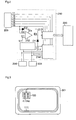
- Fig. 1 is a schematic circuit diagram showing the integrated circuit card according to a preferred embodiment of the present invention.
- the IC card is a dual mode type IC card that operates in both a contact-free mode and a contact mode.
- the contact-free mode is a mode where electrical energy is supplied from a reader/writer by an inductive coupling and a data transmission between the IC card and the reader/writer is performed by the inductive coupling.
- the contact mode is a mode where electrical energy is supplied from the reader/writer via a contact terminal of the IC card and the data transmission is performed via the contact terminal.
- the IC card includes a coil 111 and a contact field 160.
- the coil 111 is inductively coupled the IC card to the reader/writer in the contact-free mode.
- the contact field 160 includes contact terminals 161 through 165 each of which is contacted with a corresponding terminal of the reader/writer in the contact mode.
- the coil 111 receives electrical energy from the reader/writer based on the electromagnetic induction effect and performs a bi-directional data transmission between the IC card and the reader/writer.
- a resonance capacitor 112 is connected to the coil 111 in parallel.
- the constant values of the coil 111 and the capacitor 112 are set at predetermined values so that the values are tuned to a frequency of a carrier wave CAR serving as power supply voltage and data supplied from the reader/writer.
- the carrier wave CAR is obtained by an amplitude modulation that is modulated a sinewave of 13.56MHz by a 106kb/s data signal.
- the degree of modulation in this case is set at about 10%.
- the power supply voltage is transmitted by a carrier component of the carrier wave.
- the data is transmitted by the amplitude modulation component.
- the coil 111 and the capacitor 112 are connected to a voltage rectification part 120 for performing a full-wave rectification.
- the voltage rectification part 120 is comprised of four diodes 121 through 124 which are connected in a bridged form.
- a positive output + of the voltage rectification part 120 is connected to a smoothing capacitor 125 and a power supply part 126.
- a negative output ⁇ of the voltage rectification part 120 is connected to a ground potential GND.
- the power supply part 126 receives a direct voltage DCV obtained from the positive output + of the voltage rectification part 120 and generates a power supply voltage VCC having a constant level to supply to circuits in the IC card. That is, the power supply part 126 functions as a constant voltage generator.
- the positive output + of the voltage rectification part 120 and one end of the coil 111 are connected to a carrier detection part 130.
- the carrier detection part 130 detects whether the effective carrier wave CAR is received.
- the carrier detection part 130 includes resistors 131 and 132 which divides a voltage induced in the coil 111.
- a node between the resistor 131 and the resistor 132 is connected to a gate of an N channel type MOS transistor 133 (it is hereinafter referred to as an NMOS).
- a source and a drain of the NMOS 133 are connected to the ground potential GND and a node N1, respectively.
- a resistor 134 serving as a load and a capacitor 135 for by-passing a frequency of the carrier wave CAR are connected between the node N1 and the positive output + of the voltage rectification part 120 in parallel.
- the node N1 is connected to a gate of a P type MOS transistor 136 (it is hereinafter referred to as a PMOS) and a gate of an NMOS 137.
- a source and a drain of the PMOS 136 are connected to the positive output + of the voltage rectification part 120 and a node N2, respectively.
- a drain and a source of the NMOS 137 are connected to the node N2 and the ground potential GND, respectively.
- a carrier detection signal CARD is output from the node N2.
- the node N2 is coupled to a first input terminal of a mode direction circuit 140.
- the mode direction circuit 140 is made up of an inverter 141 and an OR circuit 142.
- a demodulator 143 is connected to the positive output + of the voltage rectification part 120.
- the demodulator 143 demodulates data component in the direct voltage DCV which is full-wave rectified by the voltage rectification part 120.
- the demodulator 143 outputs the demodulated data as transmitted data to a central processing unit 150 (CPU).
- CPU central processing unit
- the contact field 160 includes contact terminals 161 through 165. These contact terminals are electrically or mechanically contacted with corresponding terminals of the reader/writer in the contact mode and have function of receiving electrical energy or signals.
- the contact terminal 161 is a terminal that receives electrical energy via the contacted terminal of the reader/writer in the contact mode. Since the contact terminal 161 is connected to an output terminal of the power supply part 126, the power supply voltage VCC from the reader/writer is supplied to circuits in the IC card in the contact mode.
- the contact terminal 162 is a terminal that receives the ground potential GND via the contacted terminal of the reader/writer in the contact mode.
- the contact terminal 162 Since the contact terminal 162 is connected to a common node of the circuits in the IC card, ground potential GND from the reader/writer is supplied to the circuits in the IC card in the contact mode as well as the power supply voltage VCC.
- the contact terminal 165 is connected to the CPU 150.
- the bi-directional data transmission between the CPU 150 and reader/writer is executed via the contact terminal 165.
- the data are preferably transmitted to/from the CPU in serial.
- the contact terminal 163 is a terminal that receives a clock signal CLK.
- the clock signal CLK is a control signal which is supplied from the reader/writer and has a constant frequency, for example 5MHz.
- the circuits in the IC card operate based on the clock signal CLK.
- the contact terminal 164 is a terminal that receives a reset signal /RST. (" / " designates inverse of the reset signal RST)
- the reset signal /RST is the control signal from the reader/writer.
- the reset signal /RST is a L level
- the IC card is set to a reset state and thus operation is halted.
- the reset signal /RST is an H level
- the IC card is set to an operation state and thus IC card can operate.
- the contact terminals 163 and 164 are connected to the ground potential GND via pull-down resistors 166 and 167.
- the contact terminals 163 and 164 are further connected to a clock detection part 170.
- the clock detection part 170 has an inverter 171 and a NOR circuit 172.
- An input terminal of the inverter 171 is connected to the contact terminal 163.
- An output terminal of the inverter 171 is connected to a first input terminal of the NOR circuit 172.
- a second input terminal of the NOR circuit 172 is connected to the contact terminal 164.
- An output terminal of the NOR circuit 172 is connected to a gate of an NMOS 73.
- a source and a drain of the NMOS 73 are connected to the ground potential GND and a node N3, respectively.
- the node N3 is connected to the power supply voltage VCC via a load resistor 174 and a capacitor 175 for bypassing a component of the clock frequency.
- the node N3 is further connected to an inverter 176 which outputs a clock detection signal CLKD.
- the clock detection signal CLKD output from the inverter 176 and the reset signal /RST applied to the contact terminal 164 are applied to second and third input terminals of the mode direction circuit 140.
- the mode direction circuit 140 outputs a mode signal MOD.
- the CPU 150 receives the mode signal MOD.
- the mode signal MOD is set to the L level in the contact-free mode and is set to the H level in the contact mode.
- the IC card of the preferred embodiment further has a memory part 180 connected to the CPU 150, such as read only memory (ROM), electrical programmable read only memory (EPROM).
- the IC card also has a modulator for outputting a transmission data to the coil 111 in the contact-free mode and a clock signal regeneration part for regenerating a clock signal from the carrier wave CAR and outputting the regenerated clock signal to the CPU 150.
- ROM read only memory
- EPROM electrical programmable read only memory
- the IC card also has a modulator for outputting a transmission data to the coil 111 in the contact-free mode and a clock signal regeneration part for regenerating a clock signal from the carrier wave CAR and outputting the regenerated clock signal to the CPU 150.
- ROM read only memory
- EPROM electrical programmable read only memory
- the IC card also has a modulator for outputting a transmission data to the coil 111 in the contact-free mode and a clock signal regeneration part for regenerating a clock signal from the carrier
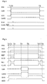
- Fig. 3 is a perspective view of the IC card shown in Fig. 1.
- the IC card is made up of a body 301 made of plastic, an IC chip and the contact field 160.
- the body 301 has 54 millimeters in length, 86 millimeters in width and 0.76 millimeters in thickness.
- the coil 111, and the IC chip and the contact field 160 are embedded in the body 301.
- the CPU 150, the memory part 180, the voltage rectification part 120, the power supply part 126, the carrier detection part 130, the mode direction circuit 140, the clock detection part 180, and so on are integrated into the IC chip.
- the IC chip is adhered to a back surface of the contact field 160. Electrodes of the IC chip are wire bonded to corresponding contact terminals of the contact field 160.
- the contact field 160 is disposed at a predetermined location on the IC card so as to satisfy a standardized location. Besides, the size of the coil and the location at which the coil 111 is formed are depended on the circumstances. In Fig. 3, a triple curled coil 111 is patterned at the periphery of the body 301. Thus, even though the distance between the reader/writer and the IC card is set at 10 centimeters in the contact-free mode, normal contact-free mode operation can be performed.
- Fig. 4 is a timing chart showing an operation of the IC card according to the present invention in the contact-free mode.
- Fig. 5 is a timing chart showing an operation of the IC card according to the present invention in the contact mode.
- the coil 111 is magnetically coupled to the coils of the reader/writer.
- the contact terminals of the contact field160 are not connected any terminals of the reader/writer.
- the carrier wave CAR output from the reader/writer is received at a tuning circuit comprised of the coil 111 and the capacitor 112 at the time T1
- the received carrier wave CAR is full-wave rectified by the voltage rectification part 120.
- the direct voltage DCV at the positive output + of the voltage rectification part 120 increases.
- the direct voltage DCV is supplied to the carrier detection part 130 as a power supply voltage.
- the voltage supply part 126 outputs the power supply voltage VCC.
- the power supply voltage VCC is supplied to the circuits in the IC card.
- the carrier wave CAR received at coil 111 is divided into a predetermined voltage level by the resistors 131 and 132 in the carrier detection part 130.
- the divided voltage level of the carrier wave CAR is applied to the gate of the NMOS 133.
- the NMOS 133 turns on/off in response to the frequency of the clock signal CLK. Since the resistor 134 and the capacitor 135 are connected to the NMOS 133 as load, the node N1 is maintained at the L level during the carrier wave CAR is applied to the carrier detection part 130.
- the carrier detection signal CARD output from the node N2 is set at the H level.
- the carrier detection signal CARD is inverted by the inverter 141 and thus a signal S141 having the L level is transferred to the OR circuit 142.
- the contact terminals 163 and 164 are pull-downed to the ground potential via the resistors 166 and 167. That is, the contact terminals 163 and 164 are set at the L level. Since the inverter 171 outputs the H level based on the L level of the contact terminal 163, the NOR circuit 172 outputs the L level. Then the NMOS 173 enters to the off state and the node N3 is set at the H level. As a result, the inverter 176 outputs the clock detection signal CLKD having L level to the mode direction circuit 140.
- the OR circuit 142 outputs the mode signal MOD having the L level.
- the operation mode of the CPU 150 is set at the contact-free mode in response to the received mode signal MOD having the L level.
- the contact terminals 161 through 165 of the contact field 160 are contacted with the terminals of the reader/writer.
- the carrier wave CAR is not applied to the coil 111.
- the power supply voltage VCC is supplied to the contact terminal 161 from the reader/writer at the time T1
- the power supply voltage VCC is supplied to the circuits in the IC card.
- the clock signal CLK applied to the contact terminal 163 and the reset signal /RST applied to the contact terminal 164 are in the L level. Therefore, the signal S172 output from the NOR circuit 172 of the clock detection part 130 goes to the L level and thus the signal at the node N3 goes to the H level. As a result, the clock detection signal CLKD goes to the L level.
- the carrier detection signal CARD is in the L level and thus the signal S141 goes to the H level. Thereby, the mode signal MOD goes to the H level. As a result, the operation mode of the CPU 150 is set to the contact mode.
- the NOR circuit 172 When the supply of the clock signal CLK to the contact terminal 163 is started at the time t2, the NOR circuit 172 outputs the signal S172 as the clock signal CLK. Thereby, the NMOS 173 tuns on/off in response to the frequency of the clock signal CLK. Since the resistor 174 and the capacitor 175 are connected to the NMOS 173 as a load, the node N3 is maintained at the L level during the H level of the signal S172 is applied to the gate of the NMOS 173. Thus, the clock detection signal CLKD is set to the H level in this time period. At this time, since the mode signal MOD is already set to the H level, the contact mode is not changed.
- the NOR circuit 172 outputs the signal S172 having the L level. Thereby, the NMOS 173 is changed to the off state and thus the detection of the clock signal CLK is stopped. The node N3 and the clock detection signal CLKD are changed to the L level. At this time, since the reset signal /RST and the signal S141 are set to the H level, the contact mode is not changed.
- the direct voltage DCV is applied to the carrier detection part 130 because the strong alternating signal (the carrier wave CAR) is induced in the coil 111. Since the carrier detection signal CARD is changed to the H level in response to the direct voltage DCV, the signal S141 is changed to the L level. However, since the reset signal /RST is already set to the H level, that is, the mode signal MOD is set to the H level, the contact mode is not changed.
- the NOR circuit 172 outputs the signal S172 as the clock signal CLK. Since the node N3 is changed to the L level, the clock detection signal CLKD is set to the H level. However, since the mode signal MOD is in the H level, the contact mode is not changed.
- the NOR circuit 172 outputs the signal S172 having the L level. Thereby, the node N3 is set to the H level and the clock detection signal CLKD is set to the L level. At this time, since the carrier detection signal CARD is in the L level (the signal S141 is in the H level), the mode signal MOD is maintained at the H level. That is, the contact mode is not changed.
- the clock detection signal CLKD and the reset signal /RST are given priority to the carrier detection signal CARD.
- the mode direction circuit which receives the carrier detection signal CARD, the clock detection signal CLKD and the reset signal /RST are explained as an example to give the priority.
- the clock detection part 170 includes the NOR circuit 172 that outputs (or transfers) the clock signal CLK when the reset signal /RST having the L level and does not output (or transfer) the clock signal CLK when the reset signal /RST having the H level (that is, the detection of the clock signal CLK is stopped).
- the NOR circuit 172 that outputs (or transfers) the clock signal CLK when the reset signal /RST having the L level and does not output (or transfer) the clock signal CLK when the reset signal /RST having the H level (that is, the detection of the clock signal CLK is stopped).
- the present invention is not limited to the above-explained preferred embodiment.
- the present invention can include the following modifications.
- the modifications (a) through (e) exist as the modified circuit schemes.
- the present invention has a mode direction circuit which can direct the contact mode even if an undesirable electric magnetic induction occurs in the coil when the IC card receives the reset signal or the clock signal during the contact mode. Therefore, since the contact mode is prior to the contact-free mode during the IC card operates in the contact mode, the contact mode is not changed by the undesirable electric magnetic induction.
Landscapes
- Engineering & Computer Science (AREA)
- Computer Hardware Design (AREA)
- Microelectronics & Electronic Packaging (AREA)
- Physics & Mathematics (AREA)
- General Physics & Mathematics (AREA)
- Theoretical Computer Science (AREA)
- Computer Networks & Wireless Communication (AREA)
- Credit Cards Or The Like (AREA)
- Near-Field Transmission Systems (AREA)
Abstract
Description
Claims (6)
- An integrated circuit card comprising:a contact terminal which is to be contacted with an external device and which receives a first control signal from the external device;a first control signal detection circuit which is coupled to the contact terminal, which detects the first control signal and which outputs a first detection signal;a coil which is to be magnetically coupled to the external device and which receives a second control signal from the external device;a second control signal detection circuit which is coupled to the coil, which detects the second control signal and which outputs a second detection signal;a mode direction circuit which receives the first and second detection signals and outputs a mode signal designating a contact-free mode and a contact mode, wherein the mode direction circuit outputs the mode signal designating the contact-free mode when the first detection signal is in an inactive state and the second detection signal is in an active state and wherein the mode direction circuit outputs the mode signal designating the contact mode regardless of the state of the second detection signal when the first detection signal is in the active state; anda processing circuit which receives the mode signal and which performs a predetermined operation based on the contact mode and the contact-free mode designated by the mode signal.
- An integrated circuit card comprising:a plurality of terminals for receiving data, a first control signal and a power supply by mechanical contact to the terminals;a coil for receiving data, a second control signal and a power supply by electromagnetic induction;a mode designating circuit for designating a contact mode prior to the second control signal during the first control signal is received therein and for designating a contact-free mode during the second control signal is received therein;a processing circuit for operating in the contact mode based on the contact mode designated by the mode designating circuit and for operating in the contact-free mode based on the contact-free mode designated by the mode designating circuit.
- An integrated circuit comprising:a first node which is to be contacted with an external device and which receives a first control signal from the external device;a first control signal detection circuit which is coupled to the first node, which detects the first control signal and which outputs a first detection signal;a second node which is to be coupled to a coil and which receives a second control signal from the external device via the coil and wherein the coil is to be magnetically coupled to the external device;a second control signal detection circuit which is coupled to the second node, which detects the second control signal and which outputs a second detection signal;a mode direction circuit which receives the first and second detection signals and outputs a mode signal designating a contact-free mode and a contact mode, wherein the mode direction circuit outputs the mode signal designating the contact-free mode when the first detection signal is in an inactive state and the second detection signal is in an active state and wherein the mode direction circuit outputs the mode signal designating the contact mode regardless of the state of the second detection signal when the first detection signal is in the active state; anda processing circuit which receives the mode signal and which performs a predetermined operation based on the contact mode and the contact-free mode designated by the mode signal.
- The integrated circuit card as set forth in any of the claims 1 to 3, wherein the mode direction circuit comprises a logic circuit which has a first input terminal for receiving the second detection signal and a second input terminal for receiving the first detection signal and an output terminal for outputting the mode signal.
- The integrated circuit as set forth in any of the claims 1 to 4, wherein the first control signal is a clock signal.
- The integrated circuit as set forth in any of the claims 1 to 4, wherein the first control signal is a reset signal.
Applications Claiming Priority (2)
| Application Number | Priority Date | Filing Date | Title |
|---|---|---|---|
| JP2000208556A JP3657178B2 (en) | 2000-07-10 | 2000-07-10 | IC card |
| JP2000208556 | 2000-07-10 |
Publications (3)
| Publication Number | Publication Date |
|---|---|
| EP1179806A2 true EP1179806A2 (en) | 2002-02-13 |
| EP1179806A3 EP1179806A3 (en) | 2002-09-25 |
| EP1179806B1 EP1179806B1 (en) | 2010-02-17 |
Family
ID=18705116
Family Applications (1)
| Application Number | Title | Priority Date | Filing Date |
|---|---|---|---|
| EP01115945A Expired - Lifetime EP1179806B1 (en) | 2000-07-10 | 2001-06-29 | Intergrated circuit card |
Country Status (4)
| Country | Link |
|---|---|
| US (1) | US6572023B2 (en) |
| EP (1) | EP1179806B1 (en) |
| JP (1) | JP3657178B2 (en) |
| DE (1) | DE60141312D1 (en) |
Cited By (2)
| Publication number | Priority date | Publication date | Assignee | Title |
|---|---|---|---|---|
| EP1367532A1 (en) * | 2002-05-23 | 2003-12-03 | Sharp Kabushiki Kaisha | Contact/non-contact IC card |
| EP1496470A1 (en) * | 2003-07-09 | 2005-01-12 | St Microelectronics S.A. | Dual-mode chip card |
Families Citing this family (22)
| Publication number | Priority date | Publication date | Assignee | Title |
|---|---|---|---|---|
| JP2003132313A (en) * | 2001-10-24 | 2003-05-09 | Toshiba Corp | LSI for combination card, combination card and method of using combination card |
| US20030230631A1 (en) * | 2002-06-17 | 2003-12-18 | Hitachi, Ltd. | IC card |
| DE10311966A1 (en) * | 2003-03-18 | 2004-12-16 | Infineon Technologies Ag | smart card |
| JP4124692B2 (en) | 2003-04-25 | 2008-07-23 | シャープ株式会社 | Nonvolatile semiconductor memory device |
| US7237719B2 (en) * | 2003-09-03 | 2007-07-03 | Stmicroelectronics, Inc. | Method and apparatus for a USB and contactless smart card device |
| JP2006172121A (en) * | 2004-12-15 | 2006-06-29 | Toshiba Corp | Card-like storage device and its adapter and host device |
| US8248141B2 (en) | 2005-07-08 | 2012-08-21 | Med-El Elekromedizinische Geraete Gmbh | Data and power system based on CMOS bridge |
| CH701169B1 (en) * | 2006-10-09 | 2010-12-15 | Legic Identsystems Ag | Device for operation of a read / write device. |
| JP4675976B2 (en) * | 2008-01-15 | 2011-04-27 | シャープ株式会社 | COMBINATION TYPE IC CARD AND COMMUNICATION TYPE IC CARD COMMUNICATION METHOD |
| JP4640451B2 (en) | 2008-06-06 | 2011-03-02 | ソニー株式会社 | Contact / non-contact composite IC card, communication method, program, and communication system |
| WO2010101575A1 (en) | 2009-03-06 | 2010-09-10 | Med-El Elektromedizinische Geraete Gmbh | Data and power system based on cmos bridge |
| KR101546071B1 (en) * | 2009-05-21 | 2015-08-20 | 삼성전자주식회사 | Chip card with contact and contactless modes and operating method of the same |
| JP5347813B2 (en) * | 2009-08-03 | 2013-11-20 | ソニー株式会社 | Communication apparatus and communication method |
| DE102011108876B4 (en) * | 2011-07-28 | 2018-08-16 | Technische Universität Dresden | Direct conversion X-ray detector with radiation protection for the electronics |
| USD758372S1 (en) * | 2013-03-13 | 2016-06-07 | Nagrastar Llc | Smart card interface |
| USD759022S1 (en) | 2013-03-13 | 2016-06-14 | Nagrastar Llc | Smart card interface |
| USD729808S1 (en) | 2013-03-13 | 2015-05-19 | Nagrastar Llc | Smart card interface |
| US9647997B2 (en) | 2013-03-13 | 2017-05-09 | Nagrastar, Llc | USB interface for performing transport I/O |
| US9888283B2 (en) | 2013-03-13 | 2018-02-06 | Nagrastar Llc | Systems and methods for performing transport I/O |
| USD780763S1 (en) | 2015-03-20 | 2017-03-07 | Nagrastar Llc | Smart card interface |
| USD864968S1 (en) | 2015-04-30 | 2019-10-29 | Echostar Technologies L.L.C. | Smart card interface |
| KR102822041B1 (en) * | 2020-06-25 | 2025-06-18 | 삼성전자주식회사 | Internal voltage generation circuit of smart card and smart card including the same |
Family Cites Families (7)
| Publication number | Priority date | Publication date | Assignee | Title |
|---|---|---|---|---|
| DE3935364C1 (en) | 1989-10-24 | 1990-08-23 | Angewandte Digital Elektronik Gmbh, 2051 Brunstorf, De | |
| JP3360002B2 (en) * | 1996-03-14 | 2002-12-24 | 沖電気工業株式会社 | Contact / non-contact IC card and contact / non-contact IC card reader / writer |
| JP4212656B2 (en) * | 1997-09-23 | 2009-01-21 | エヌエックスピー ビー ヴィ | Dual mode data carrier and circuit with improved mode switching for such data carrier |
| EP0939935B1 (en) * | 1997-09-23 | 2008-08-13 | Nxp B.V. | Dual-mode data carrier and circuit for such a data carrier with potential equalizing means for equalizing the potentials of at least two contact terminals |
| CN1122936C (en) * | 1997-10-22 | 2003-10-01 | 皇家菲利浦电子有限公司 | Dual mode data carrier and circuitry for this data carrier with simplified data transfer means |
| DE19834079A1 (en) * | 1998-02-21 | 1999-09-09 | Orga Kartensysteme Gmbh | Communication between smart card and contact or non contact terminal |
| ATE345539T1 (en) * | 1998-03-24 | 2006-12-15 | Toshiba Kk | IC CARD WITH CONTACT AND CONTACTLESS INTERFACES |
-
2000
- 2000-07-10 JP JP2000208556A patent/JP3657178B2/en not_active Expired - Lifetime
-
2001
- 2001-06-29 US US09/893,502 patent/US6572023B2/en not_active Expired - Lifetime
- 2001-06-29 DE DE60141312T patent/DE60141312D1/en not_active Expired - Fee Related
- 2001-06-29 EP EP01115945A patent/EP1179806B1/en not_active Expired - Lifetime
Cited By (4)
| Publication number | Priority date | Publication date | Assignee | Title |
|---|---|---|---|---|
| EP1367532A1 (en) * | 2002-05-23 | 2003-12-03 | Sharp Kabushiki Kaisha | Contact/non-contact IC card |
| SG108922A1 (en) * | 2002-05-23 | 2005-02-28 | Sharp Kk | Combination-type ic card |
| EP1496470A1 (en) * | 2003-07-09 | 2005-01-12 | St Microelectronics S.A. | Dual-mode chip card |
| US7472834B2 (en) | 2003-07-09 | 2009-01-06 | Stmicroelectronics S.A. | Dual-mode smart card |
Also Published As
| Publication number | Publication date |
|---|---|
| JP2002024786A (en) | 2002-01-25 |
| US20020003168A1 (en) | 2002-01-10 |
| EP1179806B1 (en) | 2010-02-17 |
| US6572023B2 (en) | 2003-06-03 |
| JP3657178B2 (en) | 2005-06-08 |
| DE60141312D1 (en) | 2010-04-01 |
| EP1179806A3 (en) | 2002-09-25 |
Similar Documents
| Publication | Publication Date | Title |
|---|---|---|
| EP1179806B1 (en) | Intergrated circuit card | |
| TW387190B (en) | A device for exchanging data gy contactless communication between a terminal and remotely powered portable objects | |
| AU722833B2 (en) | Microcircuit with contact and contactless operating modes | |
| JP3885922B2 (en) | Semiconductor chip and IC card and RFID using the same | |
| US8872385B2 (en) | Wireless power transmission system | |
| JP4822588B2 (en) | Information processing apparatus and information processing device | |
| JPH10505932A (en) | Chip card | |
| JP4332963B2 (en) | Capacitive modulation of electromagnetic transponders | |
| US20070284451A1 (en) | Integrated circuit, non-contact IC card, reader/writer, wireless communications method, and computer program | |
| JP4558259B2 (en) | Combination IC card | |
| JP3867854B2 (en) | Electromagnetic inductive coupling device | |
| JP2002522850A (en) | Chip card with increased card security | |
| US7681060B2 (en) | Semiconductor integrated circuit device and IC card equipped with the same having transistor switch for disconnecting contact power during contactless mode | |
| JP4212656B2 (en) | Dual mode data carrier and circuit with improved mode switching for such data carrier | |
| JP2003296683A (en) | Non-contact IC card | |
| UA54501C2 (en) | Data carrier with contactless element for data communication and power supply, for example a chip card | |
| JP4759053B2 (en) | Non-contact type electronic device and semiconductor integrated circuit device mounted thereon | |
| JP2001160122A (en) | Non-contact IC card | |
| JP2006180491A (en) | Electromagnetic transponder with no autonomous power supply | |
| JPH0423092A (en) | IC card | |
| JP4067658B2 (en) | Data transceiver | |
| US10083386B2 (en) | Smart objects | |
| JPH1153491A (en) | Data carrier system | |
| KR20030018307A (en) | Smart card | |
| JP2007306240A (en) | Integrated circuit, noncontact ic card, information processing terminal, radio communication method and computer program |
Legal Events
| Date | Code | Title | Description |
|---|---|---|---|
| PUAI | Public reference made under article 153(3) epc to a published international application that has entered the european phase |
Free format text: ORIGINAL CODE: 0009012 |
|
| AK | Designated contracting states |
Kind code of ref document: A2 Designated state(s): AT BE CH CY DE DK ES FI FR GB GR IE IT LI LU MC NL PT SE TR |
|
| AX | Request for extension of the european patent |
Free format text: AL;LT;LV;MK;RO;SI |
|
| PUAL | Search report despatched |
Free format text: ORIGINAL CODE: 0009013 |
|
| AK | Designated contracting states |
Kind code of ref document: A3 Designated state(s): AT BE CH CY DE DK ES FI FR GB GR IE IT LI LU MC NL PT SE TR |
|
| AX | Request for extension of the european patent |
Free format text: AL;LT;LV;MK;RO;SI |
|
| 17P | Request for examination filed |
Effective date: 20030325 |
|
| AKX | Designation fees paid |
Designated state(s): DE FR GB |
|
| 17Q | First examination report despatched |
Effective date: 20070125 |
|
| GRAP | Despatch of communication of intention to grant a patent |
Free format text: ORIGINAL CODE: EPIDOSNIGR1 |
|
| GRAS | Grant fee paid |
Free format text: ORIGINAL CODE: EPIDOSNIGR3 |
|
| GRAA | (expected) grant |
Free format text: ORIGINAL CODE: 0009210 |
|
| AK | Designated contracting states |
Kind code of ref document: B1 Designated state(s): DE FR GB |
|
| REG | Reference to a national code |
Ref country code: GB Ref legal event code: FG4D |
|
| REF | Corresponds to: |
Ref document number: 60141312 Country of ref document: DE Date of ref document: 20100401 Kind code of ref document: P |
|
| PLBE | No opposition filed within time limit |
Free format text: ORIGINAL CODE: 0009261 |
|
| STAA | Information on the status of an ep patent application or granted ep patent |
Free format text: STATUS: NO OPPOSITION FILED WITHIN TIME LIMIT |
|
| 26N | No opposition filed |
Effective date: 20101118 |
|
| REG | Reference to a national code |
Ref country code: FR Ref legal event code: ST Effective date: 20110228 |
|
| PG25 | Lapsed in a contracting state [announced via postgrant information from national office to epo] |
Ref country code: DE Free format text: LAPSE BECAUSE OF NON-PAYMENT OF DUE FEES Effective date: 20110101 |
|
| PG25 | Lapsed in a contracting state [announced via postgrant information from national office to epo] |
Ref country code: FR Free format text: LAPSE BECAUSE OF NON-PAYMENT OF DUE FEES Effective date: 20100630 |
|
| PGFP | Annual fee paid to national office [announced via postgrant information from national office to epo] |
Ref country code: GB Payment date: 20110629 Year of fee payment: 11 |
|
| GBPC | Gb: european patent ceased through non-payment of renewal fee |
Effective date: 20120629 |
|
| PG25 | Lapsed in a contracting state [announced via postgrant information from national office to epo] |
Ref country code: GB Free format text: LAPSE BECAUSE OF NON-PAYMENT OF DUE FEES Effective date: 20120629 |