EP1178609A2 - Phase detector - Google Patents
Phase detector Download PDFInfo
- Publication number
- EP1178609A2 EP1178609A2 EP01000263A EP01000263A EP1178609A2 EP 1178609 A2 EP1178609 A2 EP 1178609A2 EP 01000263 A EP01000263 A EP 01000263A EP 01000263 A EP01000263 A EP 01000263A EP 1178609 A2 EP1178609 A2 EP 1178609A2
- Authority
- EP
- European Patent Office
- Prior art keywords
- digital
- fractional phase
- signal
- phase detector
- clock
- Prior art date
- Legal status (The legal status is an assumption and is not a legal conclusion. Google has not performed a legal analysis and makes no representation as to the accuracy of the status listed.)
- Granted
Links
Images


Classifications
-
- H—ELECTRICITY
- H03—ELECTRONIC CIRCUITRY
- H03L—AUTOMATIC CONTROL, STARTING, SYNCHRONISATION OR STABILISATION OF GENERATORS OF ELECTRONIC OSCILLATIONS OR PULSES
- H03L7/00—Automatic control of frequency or phase; Synchronisation
- H03L7/06—Automatic control of frequency or phase; Synchronisation using a reference signal applied to a frequency- or phase-locked loop
- H03L7/08—Details of the phase-locked loop
- H03L7/085—Details of the phase-locked loop concerning mainly the frequency- or phase-detection arrangement including the filtering or amplification of its output signal
-
- H—ELECTRICITY
- H03—ELECTRONIC CIRCUITRY
- H03L—AUTOMATIC CONTROL, STARTING, SYNCHRONISATION OR STABILISATION OF GENERATORS OF ELECTRONIC OSCILLATIONS OR PULSES
- H03L7/00—Automatic control of frequency or phase; Synchronisation
- H03L7/06—Automatic control of frequency or phase; Synchronisation using a reference signal applied to a frequency- or phase-locked loop
- H03L7/08—Details of the phase-locked loop
- H03L7/085—Details of the phase-locked loop concerning mainly the frequency- or phase-detection arrangement including the filtering or amplification of its output signal
- H03L7/087—Details of the phase-locked loop concerning mainly the frequency- or phase-detection arrangement including the filtering or amplification of its output signal using at least two phase detectors or a frequency and phase detector in the loop
-
- H—ELECTRICITY
- H03—ELECTRONIC CIRCUITRY
- H03L—AUTOMATIC CONTROL, STARTING, SYNCHRONISATION OR STABILISATION OF GENERATORS OF ELECTRONIC OSCILLATIONS OR PULSES
- H03L7/00—Automatic control of frequency or phase; Synchronisation
- H03L7/06—Automatic control of frequency or phase; Synchronisation using a reference signal applied to a frequency- or phase-locked loop
- H03L7/08—Details of the phase-locked loop
- H03L7/085—Details of the phase-locked loop concerning mainly the frequency- or phase-detection arrangement including the filtering or amplification of its output signal
- H03L7/091—Details of the phase-locked loop concerning mainly the frequency- or phase-detection arrangement including the filtering or amplification of its output signal the phase or frequency detector using a sampling device
-
- H—ELECTRICITY
- H03—ELECTRONIC CIRCUITRY
- H03L—AUTOMATIC CONTROL, STARTING, SYNCHRONISATION OR STABILISATION OF GENERATORS OF ELECTRONIC OSCILLATIONS OR PULSES
- H03L2207/00—Indexing scheme relating to automatic control of frequency or phase and to synchronisation
- H03L2207/50—All digital phase-locked loop
Definitions
- This invention relates generally to frequency synthesizers, and more particularly to a fractional phase detector that increases the overall resolution of an integer phase-locked loop such that the quantization error of the integer phase-locked loop is corrected.
- Frequency synthesizers using analog circuit techniques are well known in the art.
- Conventional RF frequency synthesizer architectures are analog-intensive and generally require a low loop bandwidth to reduce the familiar and well-known reference or compare frequency spurs.
- Low loop bandwidths are acceptable for RF-BiCMOS and RF-SiGe processes with weak digital capabilities.
- CMOS processes and their RF-CMOS derivatives are not very compatible with frequency synthesizer designs using analog circuit techniques.
- the conventional PLL-based frequency synthesizers generally comprise analog-intensive circuitry that does not work very well in a voltage-headroom-constrained aggressive CMOS environment. Such frequency synthesizers do not take advantage of recently developed high density digital gate technology.
- Newer frequency synthesizer architectures have used sigma-delta modulated frequency divider techniques to randomize the above discussed frequency spurs by randomizing the spurious content at the cost of increased noise floor. These techniques have not significantly reduced the undesirable analog content.
- Other frequency synthesizer architectures have used direct digital synthesis (DDS) techniques that do not work at RF frequencies without a frequency conversion mechanism requiring an analog solution. Further, previous all-digital PLL architectures rely on an over-sampling clock. Such architectures cannot be used at RF frequencies.
- DDS direct digital synthesis
- the present invention is directed to a digital fractional phase detector for an all-digital phase domain PLL frequency synthesizer that is compatible with deep sub-micron CMOS processes.
- the all-digital phase domain PLL frequency synthesizer accommodates direct frequency/phase modulation transmission to remove the requirement for an additional transmitting modulator normally associated with wireless digital transmitters. This is accomplished by operating the PLL entirely in the phase domain with maximum digital processing content such that the loop can be of high-bandwidth of "type 1" without the need for a loop filter.
- a "type 1" PLL loop as used herein, means a loop having only one integrating pole in the feedback loop. Only one integrating pole exists due to the VCO frequency-to-phase conversion. It is possible therefore, to eliminate a low-pass filter between the phase detector and the oscillator tuning input, resulting in a high bandwidth and fast response of the PLL loop.
- the all-digital phase domain PLL frequency synthesizer contains only one major analog component, a digitally-controlled 2.4 GHz voltage controlled oscillator (VCO or dVCO).
- the PLL loop is an all-digital phase domain architecture whose purpose is to generate the 2.4 GHz high frequency f osc for the "BLUETOOTH" standard.
- the underlying frequency stability of the system is derived from a reference crystal oscillator, such as a 13 MHz TCXO for the global system for mobile communications (GSM) system.
- the phase of the VCO output is obtained by accumulating the number of significant (rising or falling) edge clock transitions.
- the phase of the reference oscillator is obtained by accumulating a frequency control word on every significant (rising or falling) edge of the reference oscillator output that is re-clocked via the VCO output.
- significant edge means either a “rising” or a “falling” edge.
- a ceiling element continuously adjusts a reference phase value associated with the accumulated frequency control word by rounding off to the next integer (alternatively, truncating fractional bits necessary) to compensate for fractional-period delays caused by re-clocking of the reference oscillator by the VCO output.
- phase error signal is then easily obtained by using a simple arithmetic subtraction of the VCO phase from the adjusted reference phase on every significant edge of the re-clocked reference oscillator output.
- the phase error signal can then be used as the tuning input to the digitally-controlled VCO directly via a gain element associated with the PLL loop operation.
- the phase quantization resolution cannot be better than +/- ⁇ radians of the frequency synthesizer VCO clock.
- the present digital fractional phase detector is capable of accommodating a quantization scheme to measure fractional delay differences between the significant edge of the frequency synthesizer VCO clock and an external reference oscillator clock.
- the digital fractional phase detector has a time-to-digital converter having a resolution determined by an inverter delay associated with a given CMOS process.
- the digital fractional phase is determined by passing the frequency synthesizer VCO clock through a chain of inverters such that each inverter output will produce a clock pulse slightly delayed from that of the immediately previous inverter. The resultant staggered clock phases would then be sampled by the same reference clock.
- a digital fractional phase detector system that allows fast design turn-around using automated CAD tools.
- a digital fractional phase detector system is provided to implement an all-digital phase domain PLL frequency synthesizer having much less undesirable parameter variability than normally associated with analog circuits.
- a digital fractional phase detector system is provided to implement an all-digital phase domain PLL frequency synthesizer having enhanced testability features.
- a digital fractional phase detector system is provided to implement an all-digital phase domain PLL frequency synthesizer that requires desirably low silicon area to physically implement.
- a digital fractional phase detector system is provided to implement an all-digital phase domain PLL frequency synthesizer that requires lower power than conventional frequency synthesizers.
- a digital fractional phase detection system is provided to implement an all-digital phase domain PLL frequency synthesizer having direct frequency/phase modulation transmission capability to minimize system transmitter requirements.
- a digital fractional phase detection system is provided to implement an all-digital phase domain PLL frequency synthesizer that accommodates the "BLUETOOTH" communication protocol.
- a digital fractional phase detection system is provided to increase the overall resolution of an integer phase-locked loop such that the quantization error of the integer phase-locked loop is corrected.
- Figure 1 illustrates an all-digital PLL synthesizer 100.
- the synthesizer 100 naturally combines transmitter frequency modulation capability with a wideband, all-digital PLL modulation technique to maximize digitally-intensive implementation by operating in a synchronous phase domain.
- the PLL loop utilizes an all-digital phase domain architecture capable of generating the 2.4 GHz high frequency f osc for the "BLUETOOTH" standard band.
- the all-digital phase domain PLL frequency synthesizer 100 depicted in Figure 1 contains only one major analog/RF component, a digitally-controlled 2.4 GHz voltage controlled oscillator (dVCO) 104, being a portion of a numerically-controlled oscillator (NCO) 103, that also comprises a gain element 105.
- the underlying frequency stability of the synthesizer 100 is derived from a frequency reference crystal oscillator 110, such as a 13 MHz TCXO for the GSM system.
- phase ⁇ ⁇ ( iT ⁇ ) of the dVCO 104 clock signal, CKV 114, with period T v , at time instances iT v , where i is an integer, is obtained by accumulating the number of rising- or falling-edge clock transitions generated via a sinusoidal-to-digital converter 106.
- phase ⁇ r ( kT r ) of a frequency reference clock, FREF, provided by the reference crystal oscillator ( FREF ) 110, with period T r , at time instances kT r where k is another integer, is obtained by accumulating 102 the frequency control word (FCW 116) on every rising (or falling) edge of the frequency reference clock FREF.
- FCW 116 the frequency control word
- FCW 116 can be comprised of only an integer or an integer ( N i ) and fractional ( N f ) parts.
- the dVCO 104 and the reference crystal oscillator 110 clock domains are entirely asynchronous, making it difficult to physically compare the two digital phase values ⁇ ⁇ ( iT ⁇ ) and ⁇ r ( kT r ) at different time instances iT v and kT r .
- ⁇ ⁇ ( iT ⁇ ) and ⁇ r ( kT r ) are discrete-time signals with incompatible sampling times and cannot be directly compared without some sort of interpolation. The present inventors recognized therefore, it is imperative that any digital-word comparison be performed in the same clock domain.
- This function is achieved by over-sampling the FREF reference oscillator 110 by the high-rate dVCO 104 output CKV 114, and using the resulting frequency reference clock CKR 112 to accumulate via accumulator 102 the reference phase ⁇ r ( kT r ) as well as to synchronously sample, via latch/register 120, the high-rate dVCO 104 phase ⁇ ⁇ ( iT ⁇ ).
- ⁇ r ( k ) FCW • k•T r + ⁇ ( k ) ( ⁇ 2 ⁇ • rad )
- index k is the k th transition of the re-timed reference clock CKR 112 and contains an integer number of CKV 114 clock transitions
- ⁇ ( k ) is the integer-loop quantization error, in the range of ⁇ (0,1) , that could be further corrected by other means, such as a fractional phase detector 200 discussed in more detail herein below with reference to Figures 2-6.
- the integer phase detector in the synchronous digital phase environment can now be realized as a simple arithmetic subtraction via combinatorial element 122 of the dVCO 104 phase from the reference phase performed every rising edge of the CKR clock 112.
- the reference re-timing operation can be recognized as a quantization in the dVCO 104 CKV 114 clock transitions integer domain, where each CKV 114 clock transition rising edge is the next integer. Since the synthesizer 100 must be time-causal, quantization to the next CKV 114 clock transition rising edge (next integer), rather than the closest transition (rounding-off to the closest integer), can only be realistically performed. This limitation is then compensated for in the phase domain by the ceiling element 108 associated with the reference phase since the reference phase ⁇ r ( k ) is generally a fixed-point arithmetic signal having a sufficiently large fractional part to achieve the required frequency resolution as set forth in Equation 3 above.
- a ceiling element 108 continuously adjusts a reference phase value associated with the accumulated frequency control word by rounding to the next integer (alternatively, truncating the fractional bits), thereby compensating for delays caused by re-clocking of the reference oscillator 110 by the VCO output CKV 114.
- the ceiling operation (demonstrated via Equation 7) could be easily implemented by discarding the fractional bits and incrementing the integer bits. This technique, however, improperly handles the case when the fractional part is zero, but has no practical consequences.
- this truncation process achieves a timing correction since phase is a characteristic that can be used to describe a time progression.
- phase resolution cannot be better than +/- ⁇ radians of the dVCO 104 clock, even though the foregoing integer-loop quantization error ⁇ due to reference phase retiming illustrated by Equation 5 is compensated by next-integer rounding operation (ceiling) of the reference phase.
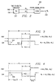
- FIG. 2 a simple block diagram illustrates a digital fractional phase detector system 200 according to one embodiment of the present invention.
- the system 200 is capable of accommodating a quantization scheme to measure fractional (sub- Tv ) delay differences between the significant edge of the dVCO 104 clock CKV 114 and the FREF oscillator 110 reference clock 112.
- the system 200 uses a time-to-digital converter (TDC) 201 with a resolution of ⁇ t ref and expresses the time difference as a digital word. Due to the dVCO 104 edge counting nature of the PLL, it can be appreciated that the phase quantization resolution cannot be better than +/- ⁇ radians as stated above. A much finer phase resolution however, is required for wireless applications such as "BLUETOOTH.” Such finer resolution must be achieved without forsaking the requisite digital signal processing capabilities.
- TDC time-to-digital converter
- FIG 8 is a simplified schematic diagram illustrating a scheme for correcting the integer-loop quantization error ⁇ (k) by means of a fractional phase detector (PDF) 804 for the all-digital PLL synthesizer 100 shown in Figure 1.
- the phase output, PHD 802 of the integer part of the PLL-loop 800 contains the fractional part of the accumulated FCW word 116, frac ( ⁇ r ), if the desired fractional division ratio FCW 116 is generally fractional-N.
- frac ( ⁇ r ) is subtracted from both the integer reference phase ⁇ r and the fractional correction ⁇ ( k ) is discussed herein below with reference to Figures 2-6, and is captured schematically on Figure 1.
- the solution illustrated in Figure 2 measures the one-sided fractional (sub- T v ) delay difference between the dVCO 104 clock CKV 114 and the FREF oscillator 110 clock 112 to express the time difference as a digital word ⁇ 202.
- the maximum readily achievable timing resolution of the digital fractional phase detector 200 is determined by an inverter delay associated with a given CMOS process, and is about 40 psec for the C035.1 CMOS process developed by Texas Instruments Incorporated of Dallas, Texas.
- the digital fractional phase is determined by passing the dVCO 104 clock CKV 114 through a chain of inverters (such as shown in Figure 5), such that each inverter output would produce a clock pulse slightly delayed from that of the immediately previous inverter.
- the resultant staggered clock phases would then be sampled by the same reference clock.
- position of the detected transition from 1 to 0 would indicate a quantized time delay ⁇ T r between the FREF 110 sampling edge and the rising edge 302 of the dVCO clock, CKV 114 in ⁇ t res multiples; and position of the detected transition from 0 to 1 would indicate a quantized time delay ⁇ T f between the FREF 110 sampling edge and the falling edge 400 of the dVCO clock, CKV 114. Because of the time-causal nature of the foregoing digital fractional phase detection process, both time delay values ⁇ T r and ⁇ T f must be interpreted as non-negative.
- Equation 9 where ⁇ t frac is the digital fractional phase detector error.
- ⁇ t r is used to calculate the ⁇ ( k ) correction of Equation 5 that is positive and ⁇ (0,1) .
- ⁇ t r has to be normalized by dividing it by the clock period, in order to properly combine it with the integer phase detector output, ⁇ d .
- fractional phase detector output ⁇ ( k ) or ⁇ F ( k ) sequence can be easily compared on a bit-by-bit basis; and since the expected output pattern is known in advance and is now in the digital format, a better alternative of a Viterbi sequence detection or a matched filter could be used. In such a scenario, the space difference between the observed and expected patterns could be output as the fractional phase error. This solution provides a system with less reference feedthrough and lower overall error.
- the present PLL loop operation can be further enhanced by taking advantage of the predictive capabilities of the all-digital PLL loop.
- the dVCO 104 does not necessarily have to follow the modulation FCW 116 command with the normal PLL loop response.
- the dVCO 104 control and the resulting phase error measurement are in numerical format, it is easy to predict the current K vco gain of the dVCO 104 by simply observing the past phase error responses to the NCO corrections. With a good estimate of the K vco gain, the normal NCO control could be augmented with the "open loop" instantaneous frequency jump estimate of the new FCW 116 command. It can be appreciated that the resulting phase error should be very small and subject to the normal closed PLL loop correction transients.
- the prediction feature is less important for channel hopping, where the allowed time is much greater.
- the foregoing prediction feature is, however, essential to realize the direct frequency synthesizer modulation in the Gaussian frequency shift keying GFSK modulation scheme of "BLUETOOTH” or GSM.
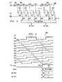
- FIG. 5 is a schematic diagram illustrating a time-to-digital converter 500 according to one embodiment of the present invention and that is suitable to implement the time delay quantization scheme depicted in Figure 2.
- the time-to-digital converter 500 includes a plurality of inverter delay elements 502 and latch/registers 504. As the dVCO clock CKV 114 continues to run, the CKV 114 delayed vector is latched into the storage elements (latch/registers 504). It is readily apparent that the converter can be formulated from any desired number of inverter delay elements 502 and latch/registers 504, within certain physical limitations, so long as the total delay of the inverter array sufficiently covers the CKV 114 clock period.
- the delayed vector characteristics are therefore dependent upon the total number of inverter delay elements 502, delay values of individual inverter delay elements 502, and associated latch/registers 504 used to formulate the time-to-digital converter 500.
- each of the latch/registers 504 will be queried in order to obtain a snapshot of the quantized fractional phase difference between the dVCO 104 clock signal CKV 114 phase and the reference clock FREF 110 signal phase.
- the accuracy of the snapshot or indication of the fractional phase difference can be seen to depend upon the single inverter delay elements.
- Figure 6 is a timing diagram 600 associated with the time-to-digital converter 500 shown in Figure 5.
- the plurality of latch/registers 504 are accessed to obtain a snapshot 604 of the delayed replicas of the dVCO clock CKV 114 relative to the rising edge of the reference oscillator FREF 110.
- the snapshot 604 can be seen to express the time difference as a digital word.
- the timing pulses 304, 404 represent dVCO output clock CKV 114 cycles that are captured in the latch/registers 504 during each significant transition of the FREF clock 110.
- the foregoing digital word is then used by the frequency synthesizer 100 to compensate for phase differences between the significant edge of the dVCO clock CKV 114 and the reference oscillator FREF 110 as discussed herein above with reference to both Figures 2-4 and equations 8-13.
- the present invention presents a significant advancement in the art of RF synthesizer circuits and associated methods.
- This invention has been described in considerable detail in order to provide those skilled in the RF synthesizer art with the information need to apply the novel principles and to construct and use such specialized components as are required.
- the present invention represents a significant departure from the prior art in construction and operation.
- particular embodiments of the present invention have been described herein in detail, it is to be understood that various alterations, modifications and substitutions can be made therein without departing in any way from the spirit and scope of the present invention, as defined in the claims which follow.
- certain embodiments set forth herein illustrate various hardware implementations
- the present invention shall be understood to also parallel structures and methods using software implementations as set forth in the claims.
Landscapes
- Stabilization Of Oscillater, Synchronisation, Frequency Synthesizers (AREA)
- Manipulation Of Pulses (AREA)
Abstract
Description




Claims (47)
- A digital fractional phase detector comprising:
a time-to-digital converter (TDC) having a plurality of delay elements associated with a first input and a plurality of latch/register elements associated with both a second input and a plurality of outputs, wherein the first input is configured to receive a first clock signal, and further wherein the second input is configured to receive a reference clock signal such that the plurality of latch/register elements can store a snapshot of a delayed replica vector of first clock signal data in response to significant edge transitions associated with the second clock. - The digital fractional phase detector according to claim 1 further comprising:
a digital edge detector having a plurality of inputs in communication with the plurality of outputs, and further having first and second outputs, wherein the edge detector is responsive to the delayed replica vector of first clock data such that the first output can generate a TDC rise-time signal associated with timing of a positive transition of the first clock and further wherein the edge detector is responsive to the stream of first clock state data such that the second output can generate a TDC fall-time signal associated with timing of a negative transition of the first clock. - The digital fractional phase detector according to claim 2 further comprising:
a normalizer element having a first input configured to receive the TDC rise-time signal and further having a second input configured to receive the TDC fall-time signal, wherein the normalizer element is responsive to the TDC rise-time signal and the TDC fall-time signal to generate a period-normalized fractional phase signal that is normalized by a clock period associated with the first clock signal. - The digital fractional phase detector according to claim 3 further comprising:
a combinatorial element configured to combine the period-normalized fractional phase signal with an accumulated frequency control word fractional phase signal and generate a fractional phase compensated signal therefrom. - The digital fractional phase detector according to any preceding claim, wherein the plurality of delay elements comprise inverters.
- The digital fractional phase detector according to claim 5, wherein the first clock signal is associated with a numerically-controlled voltage controlled oscillator.
- The digital fractional phase detector according to any preceding claim, wherein the plurality of delay elements are selected from the group consisting of buffers, a tapped delay line, and inverters.
- The digital fractional phase detector according to any preceding claim, wherein the digital fractional phase detector is configured to increase overall resolution of an integer phase-locked loop (PLL) such that a quantization error ε of the integer PLL will be corrected.
- The digital fractional phase detector according to any preceding claim, further comprising:
a digital edge detector in communication with the plurality of latch/register elements and configured to generate a first time-to-digital signal associated with a timing of a first transition of the first clock and further adapted to generate a second time-to-digital signal associated with a timing of a second transition of the first clock. - A digital fractional phase detector comprising:a first input configured to receive a first clock signal;a second input configured to receive a second clock signal; andan output, wherein the digital fractional phase detector is responsive to the first and second clock signals such that it can generate a fractional phase compensated signal therefrom at the output.
- The digital fractional phase detector according to claim 10 further comprising:
a plurality of delay elements in communication with the first input. - The digital fractional phase detector according to claim 11 wherein the plurality of delay elements comprise inverters.
- The digital fractional phase detector according to claim 11 wherein the plurality of delay elements are selected from the group consisting of buffers, a tapped delay line, and inverters.
- The digital fractional phase detector according to claim 11 further comprising:
a plurality of latch/registers in communication with the plurality of delay elements and the second input such that the plurality of latch/registers can store a delayed replica of first clock signal data in response to significant edge transitions associated with the second clock. - The digital fractional phase detector according to claim 14 further comprising:
a digital edge detector in communication with the plurality of latch/registers and configured to generate a time-to-digital rise-time signal associated with a timing of a positive transition of the first clock and further can generate a time-to-digital fall-time signal associated with a timing of a negative transition of the first clock. - The digital fractional phase detector according to claim 15 further comprising:
a normalizer element responsive to the rise-time signal and the fall-time signal to generate a period-normalized fractional phase signal that is normalized by a clock period associated with the first clock signal. - The digital fractional phase detector according to claim 16 further comprising:
a combinatorial element configured to combine the period-normalized fractional phase signal with an accumulated frequency control word fractional phase signal and generate a fractional phase compensated signal therefrom. - The digital fractional phase detector according to claim 17, wherein the first clock signal is associated with a numerically-controlled voltage controlled oscillator.
- The digital fractional phase detector according to claim 18, wherein the second clock signal is associated with a frequency reference oscillator.
- The digital fractional phase detector according to any of claims 14 to 19, further comprising:
a digital edge detector in communication with the plurality of latch/registers and configured to generate a first time-to-digital signal associated with a timing of a first transition of the first clock and further can generate a second time-to-digital signal associated with a timing of a second transition of the first clock. - The digital fractional phase detector according to claim 10, wherein the first clock signal is associated with a numerically-controlled voltage controlled oscillator.
- The digital fractional phase detector according to claim 21 wherein the second clock signal is associated with a frequency reference oscillator.
- The digital fractional phase detector according to claim 10, wherein the digital fractional phase detector is configured to increase overall resolution of an integer phase-locked loop (PLL) such that a quantization error ε of the integer PLL will be corrected.
- A digital fractional phase detector comprising:means for receiving a digitally-controlled voltage controlled oscillator (dVCO) clock signal; andmeans for receiving a frequency reference clock signal and storing a snapshot of a delayed replica of dVCO clock signal data in response to significant edge transitions associated with the frequency reference clock signal.
- The digital fractional phase detector according to claim 24 further comprising:
means for retrieving the delayed replica of dVCO clock signal data in response to the frequency reference clock signal and generating a rise-time signal and a fall-time signal therefrom. - The digital fractional phase detector according to claim 25 further comprising:
means for receiving the rise-time signal and the fall-time signal and generating a period-normalized fractional phase signal therefrom. - The digital fractional phase detector according to claim 26 further comprising:
means for combining the period-normalized fractional phase signal with an accumulated frequency control word fractional phase signal to generate a fractional phase compensated signal therefrom. - The digital fractional phase detector according to claim 24 further comprising:
means for retrieving the delayed replica of dVCO clock signal data in response to the frequency reference clock signal and generating a first time-to-digital signal and a second time-to-digital signal therefrom. - The digital fractional phase detector according to claim 28 further comprising:
means for receiving the first time-to-digital signal and the second time-to-digital signal and generating a period-normalized fractional phase signal therefrom. - The digital fractional phase detector according to claim 29 further comprising:
means for combining the period-normalized fractional phase signal with an accumulated frequency control word fractional phase signal to generate a fractional phase compensated signal therefrom. - The digital fractional phase detector according to claim 30 wherein the digital fractional phase detector is capable of increasing overall resolution of an integer phase-locked loop (PLL) such that a quantization error ε of the integer PLL can be corrected.
- A digital fractional phase detector comprising:first means for receiving a first clock signal;second means for receiving a second clock signal;third means for receiving an accumulated frequency control word fractional phase signal; andmeans for processing the first and second clock signals and the accumulated frequency control word fractional phase signal and generating a fractional phase compensated signal therefrom.
- The digital fractional phase detector according to claim 32, wherein the first receiving means comprises a plurality of delay elements.
- The digital fractional phase detector according to claim 33, wherein the plurality of delay elements are selected from the group consisting of inverters, a tapped delay line, and buffers.
- The digital fractional phase detector according to claim 34, wherein the second receiving means comprises a plurality of latch/registers.
- The digital fractional phase detector according to claim 35, wherein the third receiving means comprises a combinatorial element.
- The digital fractional phase detector according to claim 36, wherein the processing means comprises a digital edge detecting means for generating a rise-time signal associated with a positive transition of the first clock and further for generating a fall-time signal associated with a negative transition of the first clock.
- The digital fractional phase detector according to claim 37, wherein the processing means further comprises:
means for generating a period-normalized fractional phase signal that is normalized by a clock period associated with the first clock signal. - The digital fractional phase detector according to claim 38 wherein the processing means further comprises:
means for combining the period-normalized fractional phase signal and the accumulated frequency control word fractional phase signal. - The digital fractional phase detector according to claim 36 wherein the processing means comprises a digital edge detecting means for generating a first time-to-digital signal associated with a first transition of the first clock and further for generating a second time-to-digital signal associated with a second transition of the first clock.
- The digital fractional phase detector according to claim 40 wherein the processing means further comprises:
means for generating a period-normalized fractional phase signal that is normalized by a clock period associated with the first clock signal. - The digital fractional phase detector according to claim 41 wherein the processing means further comprises:
means for combining the period-normalized fractional phase signal and the accumulated frequency control word fractional phase signal. - The digital fractional phase detector according to claim 32 wherein the first clock signal is associated with a digitally-controlled voltage controlled oscillator (dVCO).
- The digital fractional phase detector according to claim 43 wherein the second clock is associated with a frequency reference oscillator.
- A digital fractional phase detector comprising:a plurality of delay elements connected in tandem, wherein each delay element has an input and an output, and further wherein the first delay element input is a VCO clock input;a plurality of latch/registers, wherein each latch/register has a first input connected to an output of a different delay element, and further wherein each latch/register has a second input configured to receive a common frequency reference clock signal, and further wherein each latch/register has an output;a digital edge detector having a plurality of inputs, wherein each edge detector input is connected to a different latch/register output, and further having a pair of outputs;a normalizer element having a pair of inputs connected to the pair of edge detector outputs, and further having an output; anda combinatorial element having an input connected to the output of the normalizer element and further having an output.
- The digital fractional phase detector according to claim 45 wherein the plurality of delay elements are selected from the group consisting of inverters, a tapped delay line, and buffers.
- The digital fractional phase detector according to claim 46 wherein the digital fractional phase detector is configured to increase overall resolution of an integer phase-locked loop (PLL) such that a quantization error ε of the integer PLL will be corrected.
Priority Applications (1)
| Application Number | Priority Date | Filing Date | Title |
|---|---|---|---|
| EP07108304.2A EP1816741B1 (en) | 2000-06-30 | 2001-07-02 | Phase detector |
Applications Claiming Priority (2)
| Application Number | Priority Date | Filing Date | Title |
|---|---|---|---|
| US608317 | 1984-05-08 | ||
| US09/608,317 US6429693B1 (en) | 2000-06-30 | 2000-06-30 | Digital fractional phase detector |
Related Child Applications (1)
| Application Number | Title | Priority Date | Filing Date |
|---|---|---|---|
| EP07108304.2A Division EP1816741B1 (en) | 2000-06-30 | 2001-07-02 | Phase detector |
Publications (3)
| Publication Number | Publication Date |
|---|---|
| EP1178609A2 true EP1178609A2 (en) | 2002-02-06 |
| EP1178609A3 EP1178609A3 (en) | 2002-10-16 |
| EP1178609B1 EP1178609B1 (en) | 2007-10-10 |
Family
ID=24435955
Family Applications (2)
| Application Number | Title | Priority Date | Filing Date |
|---|---|---|---|
| EP07108304.2A Expired - Lifetime EP1816741B1 (en) | 2000-06-30 | 2001-07-02 | Phase detector |
| EP01000263A Expired - Lifetime EP1178609B1 (en) | 2000-06-30 | 2001-07-02 | Phase detector |
Family Applications Before (1)
| Application Number | Title | Priority Date | Filing Date |
|---|---|---|---|
| EP07108304.2A Expired - Lifetime EP1816741B1 (en) | 2000-06-30 | 2001-07-02 | Phase detector |
Country Status (4)
| Country | Link |
|---|---|
| US (1) | US6429693B1 (en) |
| EP (2) | EP1816741B1 (en) |
| JP (1) | JP5021871B2 (en) |
| DE (1) | DE60130841T2 (en) |
Cited By (5)
| Publication number | Priority date | Publication date | Assignee | Title |
|---|---|---|---|---|
| FR2905040A1 (en) * | 2006-08-21 | 2008-02-22 | St Microelectronics Sa | METHOD FOR PRODUCING A DIGITAL WORD REPRESENTATIVE OF A NON-WHOLE REPORT BETWEEN THE RESPECTIVE PERIODS OF TWO SIGNALS, AND CORRESPONDING DEVICE |
| WO2009142664A1 (en) * | 2008-05-22 | 2009-11-26 | Xilinx, Inc. | Clock generation using a fractional phase detector |
| EP1844542A4 (en) * | 2005-01-31 | 2010-09-22 | Skyworks Solutions Inc | DIGITAL PHASE DETECTOR FOR A SINGLE PHASE LOOP |
| US8441323B2 (en) | 2008-09-16 | 2013-05-14 | Nxp B.V. | Signal processing using timing comparison |
| US10931290B2 (en) | 2018-03-30 | 2021-02-23 | Analog Devices International Unlimited Company | Fast settling ramp generation using phase-locked loop |
Families Citing this family (137)
| Publication number | Priority date | Publication date | Assignee | Title |
|---|---|---|---|---|
| DE10064929A1 (en) * | 2000-12-23 | 2002-07-04 | Alcatel Sa | Method and compensation module for phase compensation of clock signals |
| US6593773B2 (en) * | 2001-04-25 | 2003-07-15 | Texas Instruments Incorporated | Power saving circuitry using predictive logic |
| US7062733B1 (en) * | 2002-03-15 | 2006-06-13 | Synthesys Research, Inc. | Method and apparatus for delay line calibration |
| US6759881B2 (en) * | 2002-03-22 | 2004-07-06 | Rambus Inc. | System with phase jumping locked loop circuit |
| US7839178B2 (en) * | 2002-08-20 | 2010-11-23 | Seagate Technology Llc | High speed digital phase/frequency comparator for phase locked loops |
| US6791363B1 (en) * | 2003-03-13 | 2004-09-14 | International Business Machines Corporation | Multistage, single-rail logic circuitry and method therefore |
| US6838912B1 (en) | 2003-07-01 | 2005-01-04 | Realtek Semiconductor Corp. | Digital fractional phase detector |
| DE10345497B4 (en) * | 2003-09-30 | 2006-12-21 | Infineon Technologies Ag | Oscillator circuit, in particular for mobile communications |
| US7103110B2 (en) * | 2003-10-10 | 2006-09-05 | Atmel Corporation | Dual phase pulse modulation encoder circuit |
| US6947493B2 (en) * | 2003-10-10 | 2005-09-20 | Atmel Corporation | Dual phase pulse modulation decoder circuit |
| US7283011B2 (en) * | 2003-10-10 | 2007-10-16 | Atmel Corporation | Method for performing dual phase pulse modulation |
| EP1696564A1 (en) * | 2003-11-20 | 2006-08-30 | Advantest Corporation | Variable delay circuit |
| KR100532498B1 (en) * | 2004-01-28 | 2005-11-30 | 삼성전자주식회사 | Delay locked loop using oscillator and counter and clock synchronizing method |
| DE102004006995B4 (en) * | 2004-02-12 | 2007-05-31 | Infineon Technologies Ag | Digital phase-locked loop for sub-μ technologies |
| DE102004013929B3 (en) * | 2004-03-22 | 2005-08-11 | Infineon Technologies Ag | Control method for the reading in of a data signal to an electronic circuit input latch, especially to a DRAM circuit, whereby the delay between signal and clock flanks is set so that it is within a defined time window |
| DE102004014204B4 (en) * | 2004-03-23 | 2006-11-09 | Infineon Technologies Ag | Phase-locked loop and method for phase correction of a frequency-controllable oscillator |
| US7209065B2 (en) * | 2004-07-27 | 2007-04-24 | Multigig, Inc. | Rotary flash ADC |
| US7079577B2 (en) * | 2004-09-08 | 2006-07-18 | Atmel Corporation | Wide window decoder circuit for dual phase pulse modulation |
| US7205924B2 (en) * | 2004-11-18 | 2007-04-17 | Texas Instruments Incorporated | Circuit for high-resolution phase detection in a digital RF processor |
| US20060132340A1 (en) * | 2004-12-22 | 2006-06-22 | Lin Chun W | Apparatus and method for time-to-digital conversion and jitter-measuring apparatus using the same |
| US7212073B2 (en) * | 2005-02-02 | 2007-05-01 | Skyworks Solutions, Inc. | Capacitive tuning network for low gain digitally controlled oscillator |
| WO2006091636A2 (en) * | 2005-02-23 | 2006-08-31 | Digital Intelligence, L.L.C. | Signal decomposition and reconstruction |
| US7315270B2 (en) * | 2005-03-04 | 2008-01-01 | The Regents Of The University Of Colorado | Differential delay-line analog-to-digital converter |
| DE102005023909B3 (en) | 2005-05-24 | 2006-10-12 | Infineon Technologies Ag | Digital phase locked loop for mobile communication terminal, has correction circuit generating correction words derived from frequency correction words inputted to input of integrator and words derived from frequency word of input terminal |
| JP2007018648A (en) * | 2005-07-11 | 2007-01-25 | Elpida Memory Inc | Semiconductor device |
| US7403073B2 (en) * | 2005-09-30 | 2008-07-22 | International Business Machines Corporation | Phase locked loop and method for adjusting the frequency and phase in the phase locked loop |
| JP4850473B2 (en) * | 2005-10-13 | 2012-01-11 | 富士通セミコンダクター株式会社 | Digital phase detector |
| DE112006003542B4 (en) * | 2005-12-27 | 2016-08-04 | Analog Devices Inc. | Analog-to-digital converter system with rotary flash and process |
| US7482885B2 (en) * | 2005-12-29 | 2009-01-27 | Orca Systems, Inc. | Method of frequency synthesis for fast switching |
| US7821301B2 (en) * | 2006-01-11 | 2010-10-26 | International Business Machines Corporation | Method and apparatus for measuring and compensating for static phase error in phase locked loops |
| US7519349B2 (en) * | 2006-02-17 | 2009-04-14 | Orca Systems, Inc. | Transceiver development in VHF/UHF/GSM/GPS/bluetooth/cordless telephones |
| US7680227B2 (en) * | 2006-03-02 | 2010-03-16 | Broadcom Corporation | Method and system for filter calibration using fractional-N frequency synthesized signals |
| US7385543B2 (en) * | 2006-06-19 | 2008-06-10 | Agilent Technologies, Inc. | Systems and methods for asynchronous triggering of an arbitrary waveform generator |
| US20080013664A1 (en) * | 2006-07-11 | 2008-01-17 | Mediatek Inc. | Phase error measurement circuit and method thereof |
| WO2008033979A2 (en) * | 2006-09-15 | 2008-03-20 | Massachusetts Institute Of Technology | Gated ring oscillator for a time-to-digital converter with shaped quantization noise |
| US7826582B2 (en) * | 2006-09-18 | 2010-11-02 | National Semiconductor Corporation | Numerically controlled oscillator (NCO) output clock phase smoothing |
| DE102006050881B3 (en) * | 2006-10-27 | 2008-04-10 | Infineon Technologies Ag | Phase and frequency comparator used in digital phase-locked loop (PLL), has differential unit that has output for transmitting phase error word with predetermined word width as function of difference between counter word and integrator word |
| KR100845133B1 (en) | 2006-11-15 | 2008-07-10 | 삼성전자주식회사 | High resolution time to digital converter |
| US7427940B2 (en) * | 2006-12-29 | 2008-09-23 | Texas Instruments Incorporated | Time-to-digital converter with non-inverting buffers, transmission gates and non-linearity corrector, SOC including such converter and method of phase detection for use in synthesizing a clock signal |
| US8736323B2 (en) * | 2007-01-11 | 2014-05-27 | International Business Machines Corporation | Method and apparatus for on-chip phase error measurement to determine jitter in phase-locked loops |
| US8284822B2 (en) * | 2007-02-27 | 2012-10-09 | Broadcom Corporation | Method and system for utilizing direct digital frequency synthesis to process signals in multi-band applications |
| US20080205545A1 (en) * | 2007-02-28 | 2008-08-28 | Ahmadreza Rofougaran | Method and System for Using a Phase Locked Loop for Upconversion in a Wideband Crystalless Polar Transmitter |
| US7826550B2 (en) * | 2007-02-28 | 2010-11-02 | Broadcom Corp. | Method and system for a high-precision frequency generator using a direct digital frequency synthesizer for transmitters and receivers |
| US20080205550A1 (en) * | 2007-02-28 | 2008-08-28 | Ahmadreza Rofougaran | Method and System for Using a Phase Locked Loop for Upconversion in a Wideband Polar Transmitter |
| US8116387B2 (en) * | 2007-03-01 | 2012-02-14 | Broadcom Corporation | Method and system for a digital polar transmitter |
| KR100944497B1 (en) * | 2007-06-25 | 2010-03-03 | 삼성전자주식회사 | Digital frequency detector and digital PLL using the same |
| KR101082415B1 (en) * | 2007-07-24 | 2011-11-11 | 고려대학교 산학협력단 | Hierarchical Time to Digital Converter |
| WO2009034881A1 (en) * | 2007-09-14 | 2009-03-19 | Nec Corporation | Phase comparator and phase locked loop |
| JP4735632B2 (en) * | 2007-10-03 | 2011-07-27 | ソニー株式会社 | PLL circuit |
| CN101414823B (en) * | 2007-10-16 | 2012-08-08 | 联发科技股份有限公司 | Error Compensation Method, Digital Phase Error Elimination Module and Full Digital Phase Locked Loop |
| JP2009105651A (en) * | 2007-10-23 | 2009-05-14 | Panasonic Corp | PLL circuit and wireless communication system |
| US8045669B2 (en) * | 2007-11-29 | 2011-10-25 | Qualcomm Incorporated | Digital phase-locked loop operating based on fractional input and output phases |
| KR100993959B1 (en) | 2007-12-14 | 2010-11-11 | 한양대학교 산학협력단 | Digital Phase Locked Loops Suitable for Low Temperature Poly-Silicon Processes |
| JP2009177259A (en) * | 2008-01-21 | 2009-08-06 | Sony Corp | PLL circuit, wireless terminal device, and frequency detection method |
| US8054116B2 (en) * | 2008-01-23 | 2011-11-08 | Qualcomm Incorporated | Threshold dithering for time-to-digital converters |
| JP4729054B2 (en) * | 2008-01-28 | 2011-07-20 | 株式会社東芝 | Semiconductor integrated circuit for communication |
| US7808418B2 (en) * | 2008-03-03 | 2010-10-05 | Qualcomm Incorporated | High-speed time-to-digital converter |
| JPWO2009110172A1 (en) * | 2008-03-04 | 2011-07-14 | パナソニック株式会社 | Time digital converter, digital PLL frequency synthesizer, transmitter / receiver, receiver |
| JP5333439B2 (en) * | 2008-03-31 | 2013-11-06 | 日本電気株式会社 | Frequency synthesizer and oscillation frequency control method of oscillator |
| US8289086B2 (en) | 2008-04-02 | 2012-10-16 | Qualcomm Atheros, Inc. | Fractional and integer PLL architectures |
| JP5002528B2 (en) * | 2008-05-20 | 2012-08-15 | 株式会社日立製作所 | Digital phase detector and PLL |
| US8164493B2 (en) * | 2008-05-29 | 2012-04-24 | Realtek Semiconductor Corporation | High-resolution circular interpolation time-to-digital converter |
| US8327179B2 (en) * | 2008-06-05 | 2012-12-04 | Realtek Semiconductor Corp. | Asynchronous counter based timing error detection |
| EP2141797A1 (en) * | 2008-07-02 | 2010-01-06 | Nxp B.V. | Circuit with a time to digital converter and phase measuring method |
| JP2010034618A (en) * | 2008-07-24 | 2010-02-12 | Sony Corp | Pll circuit, radio terminal device, and control method of pll circuit |
| US7848266B2 (en) | 2008-07-25 | 2010-12-07 | Analog Devices, Inc. | Frequency synthesizers for wireless communication systems |
| US7759993B2 (en) * | 2008-08-06 | 2010-07-20 | Qualcomm Incorporated | Accumulated phase-to-digital conversion in digital phase locked loops |
| WO2010032830A1 (en) * | 2008-09-19 | 2010-03-25 | 日本電気株式会社 | Digital phase comparator and method |
| CN102187579A (en) * | 2008-10-23 | 2011-09-14 | 松下电器产业株式会社 | Digital pll circuit and communication apparatus |
| US7741917B2 (en) * | 2008-11-07 | 2010-06-22 | Telefonaktiebolaget Lm Ericsson (Publ) | Noise shaping time to digital converter |
| US8076978B2 (en) * | 2008-11-13 | 2011-12-13 | Infineon Technologies Ag | Circuit with noise shaper |
| US20110227621A1 (en) * | 2008-11-17 | 2011-09-22 | Nxp B.V. | Gain normalization of a time-to-digital converter |
| EP2192689B1 (en) * | 2008-12-01 | 2012-01-18 | Samsung Electronics Co., Ltd. | Time-to-digital converter and all-digital phase-locked loop |
| KR101632657B1 (en) * | 2008-12-01 | 2016-06-23 | 삼성전자주식회사 | Time-to-digital convertoer and all-digital phase locked loop |
| US7999707B2 (en) * | 2008-12-02 | 2011-08-16 | Electronics And Telecommunications Research Institute | Apparatus for compensating for error of time-to-digital converter |
| JP2010141519A (en) * | 2008-12-10 | 2010-06-24 | Sony Corp | Phase-locked loop and communication device |
| JP5305935B2 (en) * | 2009-01-16 | 2013-10-02 | ルネサスエレクトロニクス株式会社 | Digital phase locked loop circuit |
| US20100182049A1 (en) * | 2009-01-22 | 2010-07-22 | Henrik Sjoland | Digital Phase Detection |
| WO2010087817A1 (en) | 2009-01-27 | 2010-08-05 | Agere Systems Inc. | Critical-path circuit for performance monitoring |
| JP5284131B2 (en) | 2009-02-04 | 2013-09-11 | 株式会社東芝 | Phase synchronization circuit and receiver using the same |
| JP5321864B2 (en) * | 2009-03-10 | 2013-10-23 | 日本電気株式会社 | Digital phase comparator |
| US8283960B2 (en) * | 2009-04-27 | 2012-10-09 | Oracle America, Inc. | Minimal bubble voltage regulator |
| US8242823B2 (en) | 2009-04-27 | 2012-08-14 | Oracle America, Inc. | Delay chain initialization |
| US8198931B2 (en) * | 2009-04-27 | 2012-06-12 | Oracle America, Inc. | Fine grain timing |
| US8179165B2 (en) * | 2009-04-27 | 2012-05-15 | Oracle America, Inc. | Precision sampling circuit |
| JP5367075B2 (en) * | 2009-05-22 | 2013-12-11 | パナソニック株式会社 | PLL frequency synthesizer |
| JP2010273185A (en) * | 2009-05-22 | 2010-12-02 | Renesas Electronics Corp | Digital phase locked loop circuit |
| WO2010143241A1 (en) | 2009-06-10 | 2010-12-16 | パナソニック株式会社 | Digital pll circuit, semiconductor integrated circuit, display apparatus |
| US8604840B2 (en) * | 2009-06-25 | 2013-12-10 | Qualcomm Incorporated | Frequency synthesizer noise reduction |
| JP2011015123A (en) * | 2009-07-01 | 2011-01-20 | Kyocera Mita Corp | Electronic device and image forming apparatus |
| JP5395568B2 (en) * | 2009-08-24 | 2014-01-22 | 株式会社東芝 | Digitally controlled oscillator |
| JP2011071816A (en) * | 2009-09-28 | 2011-04-07 | Fujitsu Semiconductor Ltd | Frequency measuring circuit and PLL synthesizer having the same |
| EP2339753B1 (en) | 2009-12-24 | 2012-07-04 | Nxp B.V. | A digital phase locked loop |
| JP2011188114A (en) * | 2010-03-05 | 2011-09-22 | Toshiba Corp | Semiconductor integrated circuit |
| JP2012005022A (en) * | 2010-06-21 | 2012-01-05 | Panasonic Corp | Digital phase difference detector and frequency synthesizer having the same |
| JP5585273B2 (en) * | 2010-07-28 | 2014-09-10 | 富士通株式会社 | PLL circuit, operation method and system of PLL circuit |
| JP2012060431A (en) | 2010-09-09 | 2012-03-22 | Toshiba Corp | Time measurement circuit and digital phase synchronous circuit |
| JP5609585B2 (en) * | 2010-11-25 | 2014-10-22 | ソニー株式会社 | PLL circuit, PLL circuit error compensation method, and communication apparatus |
| WO2012153375A1 (en) * | 2011-05-06 | 2012-11-15 | 富士通株式会社 | Clock generation circuit |
| JP5776768B2 (en) | 2011-05-06 | 2015-09-09 | 富士通株式会社 | Semiconductor integrated circuit and control method thereof |
| JP2012240217A (en) * | 2011-05-16 | 2012-12-10 | Aitec:Kk | Folding type thermoplastic resin molding |
| US8862648B2 (en) | 2011-05-24 | 2014-10-14 | Taiwan Semiconductor Manufacturing Company, Ltd. | Fast filter calibration apparatus |
| US8669890B2 (en) | 2012-01-20 | 2014-03-11 | Mediatek Inc. | Method and apparatus of estimating/calibrating TDC mismatch |
| WO2013119209A1 (en) * | 2012-02-07 | 2013-08-15 | Intel Corporation | Gated ring oscillator-based digital eye width monitor for high-speed i/o eye width measurement |
| CN104170258B (en) | 2012-04-10 | 2018-09-07 | 英特尔公司 | Recycle time to digital converter device(TDC) |
| JP5872493B2 (en) * | 2012-06-13 | 2016-03-01 | 株式会社東芝 | Oscillation frequency adjustment circuit |
| US8558728B1 (en) * | 2012-07-27 | 2013-10-15 | Dust Networks, Inc. | Phase noise tolerant sampling |
| US8929499B2 (en) | 2012-09-29 | 2015-01-06 | Intel Corporation | System timing margin improvement of high speed I/O interconnect links by using fine training of phase interpolator |
| US9164134B2 (en) * | 2012-11-13 | 2015-10-20 | Nvidia Corporation | High-resolution phase detector |
| US9471091B2 (en) | 2012-11-28 | 2016-10-18 | Nvidia Corporation | Periodic synchronizer using a reduced timing margin to generate a speculative synchronized output signal that is either validated or recalled |
| DE102013101933A1 (en) * | 2013-02-27 | 2014-08-28 | Technische Universität Dresden | Method and arrangement for generating a clock signal by means of a phase locked loop |
| JP6151361B2 (en) | 2013-08-23 | 2017-06-21 | 株式会社東芝 | Wireless communication apparatus, integrated circuit, and wireless communication method |
| US9136850B2 (en) * | 2014-01-03 | 2015-09-15 | Oracle International Corporation | Phase aligner with short lock time |
| CN103957003B (en) * | 2014-04-23 | 2017-10-17 | 华为技术有限公司 | A kind of time-to-digit converter, frequency tracking apparatus and method |
| CN105526981B (en) * | 2014-09-30 | 2019-12-10 | 龙芯中科技术有限公司 | Liquid flow measuring circuit control method and device |
| JPWO2016104464A1 (en) | 2014-12-25 | 2017-06-15 | 株式会社東芝 | Phase digital converter, phase difference pulse generator, radio communication apparatus, and radio communication method |
| US9729157B2 (en) | 2015-02-13 | 2017-08-08 | Macom Technology Solutions Holdings, Inc. | Variable clock phase generation method and system |
| BR112017019570A2 (en) | 2015-04-08 | 2018-05-02 | Halliburton Energy Services Inc | system and method |
| US10523219B2 (en) | 2016-03-04 | 2019-12-31 | Sony Corporation | Phase locked loop and control method therefor |
| US9768799B1 (en) | 2016-03-21 | 2017-09-19 | Industry University Cooperation Foundation Hanyang University | Analog to digital converter including differential VCO |
| JP2017229024A (en) | 2016-06-24 | 2017-12-28 | 株式会社東芝 | Phase digital converter, wireless communication device, and wireless communication method |
| EP3291447B1 (en) * | 2016-08-30 | 2018-12-05 | Stichting IMEC Nederland | Digital phase locked loop and method for operating the same |
| US9893734B1 (en) * | 2016-10-03 | 2018-02-13 | Analog Devices Global | Adjusting phase of a digital phase-locked loop |
| US10340926B2 (en) * | 2016-10-03 | 2019-07-02 | Analog Devices Global | Fast settling sawtooth ramp generation in a phase-locked loop |
| EP3435098B1 (en) | 2017-07-25 | 2022-07-06 | Socionext Inc. | Phase measurement |
| CN107425851B (en) * | 2017-08-09 | 2021-08-06 | 京东方科技集团股份有限公司 | Frequency compensator, electronic device and frequency compensation method |
| CN109283832B (en) * | 2018-09-14 | 2020-05-12 | 东北大学 | Low-power-consumption time-to-digital converter and PHV compensation method thereof |
| US10608647B1 (en) * | 2018-12-14 | 2020-03-31 | Silicon Laboratories Inc. | Delay adjustment using frequency estimation |
| US11602311B2 (en) | 2019-01-29 | 2023-03-14 | Murata Vios, Inc. | Pulse oximetry system |
| WO2020179023A1 (en) * | 2019-03-06 | 2020-09-10 | 三菱電機株式会社 | Time-to-digital converter |
| US10727845B1 (en) * | 2019-06-25 | 2020-07-28 | Silicon Laboratories Inc. | Use of a virtual clock in a PLL to maintain a closed loop system |
| US11038523B2 (en) * | 2019-06-26 | 2021-06-15 | Intel Corporation | Ring oscillator-based analog-to-digital converter |
| US10908635B1 (en) | 2019-12-24 | 2021-02-02 | Silicon Laboratories Inc. | Detection and management of frequency errors in a reference input clock signal |
| JP7354075B2 (en) * | 2020-09-24 | 2023-10-02 | 株式会社東芝 | Phase correction device and ranging device |
| US11456750B2 (en) * | 2020-11-12 | 2022-09-27 | Mediatek Inc. | Phase-locked loop circuit having linear voltage-domain time-to-digital converter with output subrange |
| US12191862B2 (en) | 2021-12-24 | 2025-01-07 | Macom Technology Solutions Holdings, Inc. | Hybrid phase-interpolator |
| US20260005695A1 (en) | 2022-04-05 | 2026-01-01 | Sony Semiconductor Solutions Corporation | All digital phase-locked loop circuit |
Family Cites Families (9)
| Publication number | Priority date | Publication date | Assignee | Title |
|---|---|---|---|---|
| JPS61227422A (en) * | 1985-03-30 | 1986-10-09 | Toshiba Corp | Phase comparator circuit |
| US4965815A (en) * | 1988-07-21 | 1990-10-23 | U.S. Philips Corporation | Phase detection circuit for stepwise measurement of a phase relation |
| JP2868266B2 (en) * | 1990-01-25 | 1999-03-10 | 株式会社日本自動車部品総合研究所 | Signal phase difference detection circuit and signal phase difference detection method |
| JP2980267B2 (en) | 1992-01-20 | 1999-11-22 | 日本電信電話株式会社 | Phase comparison circuit and phase-locked oscillation circuit using the same |
| JPH05308263A (en) * | 1992-04-28 | 1993-11-19 | Nec Ic Microcomput Syst Ltd | Digital phase comparator |
| NL9500034A (en) * | 1995-01-06 | 1996-08-01 | X Integrated Circuits Bv | Frequency synthesis circuit. |
| US5796682A (en) * | 1995-10-30 | 1998-08-18 | Motorola, Inc. | Method for measuring time and structure therefor |
| JP3175574B2 (en) * | 1996-02-09 | 2001-06-11 | 株式会社デンソー | Time measuring device |
| US6125158A (en) * | 1997-12-23 | 2000-09-26 | Nortel Networks Corporation | Phase locked loop and multi-stage phase comparator |
-
2000
- 2000-06-30 US US09/608,317 patent/US6429693B1/en not_active Expired - Lifetime
-
2001
- 2001-06-29 JP JP2001199139A patent/JP5021871B2/en not_active Expired - Fee Related
- 2001-07-02 EP EP07108304.2A patent/EP1816741B1/en not_active Expired - Lifetime
- 2001-07-02 DE DE60130841T patent/DE60130841T2/en not_active Expired - Lifetime
- 2001-07-02 EP EP01000263A patent/EP1178609B1/en not_active Expired - Lifetime
Cited By (7)
| Publication number | Priority date | Publication date | Assignee | Title |
|---|---|---|---|---|
| EP1844542A4 (en) * | 2005-01-31 | 2010-09-22 | Skyworks Solutions Inc | DIGITAL PHASE DETECTOR FOR A SINGLE PHASE LOOP |
| FR2905040A1 (en) * | 2006-08-21 | 2008-02-22 | St Microelectronics Sa | METHOD FOR PRODUCING A DIGITAL WORD REPRESENTATIVE OF A NON-WHOLE REPORT BETWEEN THE RESPECTIVE PERIODS OF TWO SIGNALS, AND CORRESPONDING DEVICE |
| US7869555B2 (en) | 2006-08-21 | 2011-01-11 | Stmicroelectronics Sa | Digital word representative of a non-integer ratio between the respective periods of two signals |
| WO2009142664A1 (en) * | 2008-05-22 | 2009-11-26 | Xilinx, Inc. | Clock generation using a fractional phase detector |
| US7917797B2 (en) | 2008-05-22 | 2011-03-29 | Xilinx, Inc. | Clock generation using a fractional phase detector |
| US8441323B2 (en) | 2008-09-16 | 2013-05-14 | Nxp B.V. | Signal processing using timing comparison |
| US10931290B2 (en) | 2018-03-30 | 2021-02-23 | Analog Devices International Unlimited Company | Fast settling ramp generation using phase-locked loop |
Also Published As
| Publication number | Publication date |
|---|---|
| DE60130841D1 (en) | 2007-11-22 |
| DE60130841T2 (en) | 2008-07-17 |
| JP5021871B2 (en) | 2012-09-12 |
| EP1178609B1 (en) | 2007-10-10 |
| JP2002076886A (en) | 2002-03-15 |
| EP1816741B1 (en) | 2018-10-03 |
| US6429693B1 (en) | 2002-08-06 |
| EP1816741A1 (en) | 2007-08-08 |
| EP1178609A3 (en) | 2002-10-16 |
Similar Documents
| Publication | Publication Date | Title |
|---|---|---|
| EP1178609B1 (en) | Phase detector | |
| US6326851B1 (en) | Digital phase-domain PLL frequency synthesizer | |
| EP1202458B1 (en) | Method and apparatus for retiming an asynchronous clock | |
| JP5564550B2 (en) | PLL circuit | |
| EP3340468B1 (en) | Tdc, digital synthesizer, communication unit and method therefor | |
| US8830001B2 (en) | Low power all digital PLL architecture | |
| KR101632657B1 (en) | Time-to-digital convertoer and all-digital phase locked loop | |
| US8509371B2 (en) | Continuous-rate clock recovery circuit | |
| CN106341122B (en) | Phase locked loop with multi-band oscillator and method of calibrating the same | |
| US7965143B2 (en) | Digital phase detector and phase-locked loop | |
| US20110148490A1 (en) | Time-to-digital converter and all digital phase-locked loop including the same | |
| US11342925B2 (en) | Signal generation circuit and method, and digit-to-time conversion circuit and method | |
| CN101542959B (en) | Method, circuit and system for receiving data | |
| US11588491B2 (en) | Signal generation circuit and method, and digit-to-time conversion circuit and method | |
| US20120049912A1 (en) | Digital phase difference detector and frequency synthesizer including the same | |
| EP1422827A1 (en) | Low frequency self-calibration of a PLL with multiphase clocks | |
| US6838912B1 (en) | Digital fractional phase detector | |
| US11916568B2 (en) | Sampling circuit with a hierarchical time step generator | |
| US20080043894A1 (en) | Digital word representative of a non-integer ratio between the respective periods of two signals |
Legal Events
| Date | Code | Title | Description |
|---|---|---|---|
| PUAI | Public reference made under article 153(3) epc to a published international application that has entered the european phase |
Free format text: ORIGINAL CODE: 0009012 |
|
| AK | Designated contracting states |
Kind code of ref document: A2 Designated state(s): AT BE CH CY DE DK ES FI FR GB GR IE IT LI LU MC NL PT SE TR |
|
| AX | Request for extension of the european patent |
Free format text: AL;LT;LV;MK;RO;SI |
|
| RIC1 | Information provided on ipc code assigned before grant |
Free format text: 7H 03D 13/00 A, 7H 03L 7/091 B |
|
| PUAL | Search report despatched |
Free format text: ORIGINAL CODE: 0009013 |
|
| AK | Designated contracting states |
Kind code of ref document: A3 Designated state(s): AT BE CH CY DE DK ES FI FR GB GR IE IT LI LU MC NL PT SE TR |
|
| AX | Request for extension of the european patent |
Free format text: AL;LT;LV;MK;RO;SI |
|
| RIC1 | Information provided on ipc code assigned before grant |
Free format text: 7H 03D 13/00 A, 7H 03L 7/091 B, 7H 03L 7/085 B |
|
| 17P | Request for examination filed |
Effective date: 20030416 |
|
| AKX | Designation fees paid |
Designated state(s): DE FR GB |
|
| 17Q | First examination report despatched |
Effective date: 20040506 |
|
| GRAP | Despatch of communication of intention to grant a patent |
Free format text: ORIGINAL CODE: EPIDOSNIGR1 |
|
| GRAS | Grant fee paid |
Free format text: ORIGINAL CODE: EPIDOSNIGR3 |
|
| GRAA | (expected) grant |
Free format text: ORIGINAL CODE: 0009210 |
|
| AK | Designated contracting states |
Kind code of ref document: B1 Designated state(s): DE FR GB |
|
| REG | Reference to a national code |
Ref country code: GB Ref legal event code: FG4D |
|
| REF | Corresponds to: |
Ref document number: 60130841 Country of ref document: DE Date of ref document: 20071122 Kind code of ref document: P |
|
| ET | Fr: translation filed | ||
| PLBE | No opposition filed within time limit |
Free format text: ORIGINAL CODE: 0009261 |
|
| STAA | Information on the status of an ep patent application or granted ep patent |
Free format text: STATUS: NO OPPOSITION FILED WITHIN TIME LIMIT |
|
| 26N | No opposition filed |
Effective date: 20080711 |
|
| REG | Reference to a national code |
Ref country code: FR Ref legal event code: PLFP Year of fee payment: 16 |
|
| REG | Reference to a national code |
Ref country code: FR Ref legal event code: PLFP Year of fee payment: 17 |
|
| REG | Reference to a national code |
Ref country code: FR Ref legal event code: PLFP Year of fee payment: 18 |
|
| PGFP | Annual fee paid to national office [announced via postgrant information from national office to epo] |
Ref country code: FR Payment date: 20200623 Year of fee payment: 20 |
|
| PGFP | Annual fee paid to national office [announced via postgrant information from national office to epo] |
Ref country code: GB Payment date: 20200624 Year of fee payment: 20 |
|
| PGFP | Annual fee paid to national office [announced via postgrant information from national office to epo] |
Ref country code: DE Payment date: 20200622 Year of fee payment: 20 |
|
| REG | Reference to a national code |
Ref country code: DE Ref legal event code: R071 Ref document number: 60130841 Country of ref document: DE |
|
| REG | Reference to a national code |
Ref country code: GB Ref legal event code: PE20 Expiry date: 20210701 |
|
| PG25 | Lapsed in a contracting state [announced via postgrant information from national office to epo] |
Ref country code: GB Free format text: LAPSE BECAUSE OF EXPIRATION OF PROTECTION Effective date: 20210701 |