EP1178607A2 - Driving method of an electric circuit - Google Patents
Driving method of an electric circuit Download PDFInfo
- Publication number
- EP1178607A2 EP1178607A2 EP01118348A EP01118348A EP1178607A2 EP 1178607 A2 EP1178607 A2 EP 1178607A2 EP 01118348 A EP01118348 A EP 01118348A EP 01118348 A EP01118348 A EP 01118348A EP 1178607 A2 EP1178607 A2 EP 1178607A2
- Authority
- EP
- European Patent Office
- Prior art keywords
- signal
- electronic circuit
- driving method
- analog switch
- display device
- Prior art date
- Legal status (The legal status is an assumption and is not a legal conclusion. Google has not performed a legal analysis and makes no representation as to the accuracy of the status listed.)
- Granted
Links
Images






Classifications
-
- H—ELECTRICITY
- H03—ELECTRONIC CIRCUITRY
- H03K—PULSE TECHNIQUE
- H03K17/00—Electronic switching or gating, i.e. not by contact-making and –breaking
- H03K17/10—Modifications for increasing the maximum permissible switched voltage
-
- G—PHYSICS
- G09—EDUCATION; CRYPTOGRAPHY; DISPLAY; ADVERTISING; SEALS
- G09G—ARRANGEMENTS OR CIRCUITS FOR CONTROL OF INDICATING DEVICES USING STATIC MEANS TO PRESENT VARIABLE INFORMATION
- G09G3/00—Control arrangements or circuits, of interest only in connection with visual indicators other than cathode-ray tubes
- G09G3/20—Control arrangements or circuits, of interest only in connection with visual indicators other than cathode-ray tubes for presentation of an assembly of a number of characters, e.g. a page, by composing the assembly by combination of individual elements arranged in a matrix no fixed position being assigned to or needed to be assigned to the individual characters or partial characters
- G09G3/34—Control arrangements or circuits, of interest only in connection with visual indicators other than cathode-ray tubes for presentation of an assembly of a number of characters, e.g. a page, by composing the assembly by combination of individual elements arranged in a matrix no fixed position being assigned to or needed to be assigned to the individual characters or partial characters by control of light from an independent source
- G09G3/36—Control arrangements or circuits, of interest only in connection with visual indicators other than cathode-ray tubes for presentation of an assembly of a number of characters, e.g. a page, by composing the assembly by combination of individual elements arranged in a matrix no fixed position being assigned to or needed to be assigned to the individual characters or partial characters by control of light from an independent source using liquid crystals
- G09G3/3611—Control of matrices with row and column drivers
- G09G3/3648—Control of matrices with row and column drivers using an active matrix
-
- G—PHYSICS
- G09—EDUCATION; CRYPTOGRAPHY; DISPLAY; ADVERTISING; SEALS
- G09G—ARRANGEMENTS OR CIRCUITS FOR CONTROL OF INDICATING DEVICES USING STATIC MEANS TO PRESENT VARIABLE INFORMATION
- G09G3/00—Control arrangements or circuits, of interest only in connection with visual indicators other than cathode-ray tubes
- G09G3/20—Control arrangements or circuits, of interest only in connection with visual indicators other than cathode-ray tubes for presentation of an assembly of a number of characters, e.g. a page, by composing the assembly by combination of individual elements arranged in a matrix no fixed position being assigned to or needed to be assigned to the individual characters or partial characters
- G09G3/34—Control arrangements or circuits, of interest only in connection with visual indicators other than cathode-ray tubes for presentation of an assembly of a number of characters, e.g. a page, by composing the assembly by combination of individual elements arranged in a matrix no fixed position being assigned to or needed to be assigned to the individual characters or partial characters by control of light from an independent source
- G09G3/36—Control arrangements or circuits, of interest only in connection with visual indicators other than cathode-ray tubes for presentation of an assembly of a number of characters, e.g. a page, by composing the assembly by combination of individual elements arranged in a matrix no fixed position being assigned to or needed to be assigned to the individual characters or partial characters by control of light from an independent source using liquid crystals
- G09G3/3611—Control of matrices with row and column drivers
- G09G3/3685—Details of drivers for data electrodes
- G09G3/3688—Details of drivers for data electrodes suitable for active matrices only
-
- H—ELECTRICITY
- H03—ELECTRONIC CIRCUITRY
- H03K—PULSE TECHNIQUE
- H03K17/00—Electronic switching or gating, i.e. not by contact-making and –breaking
- H03K17/14—Modifications for compensating variations of physical values, e.g. of temperature
- H03K17/145—Modifications for compensating variations of physical values, e.g. of temperature in field-effect transistor switches
-
- H—ELECTRICITY
- H03—ELECTRONIC CIRCUITRY
- H03K—PULSE TECHNIQUE
- H03K17/00—Electronic switching or gating, i.e. not by contact-making and –breaking
- H03K17/51—Electronic switching or gating, i.e. not by contact-making and –breaking characterised by the components used
- H03K17/56—Electronic switching or gating, i.e. not by contact-making and –breaking characterised by the components used by the use, as active elements, of semiconductor devices
- H03K17/687—Electronic switching or gating, i.e. not by contact-making and –breaking characterised by the components used by the use, as active elements, of semiconductor devices the devices being field-effect transistors
-
- H—ELECTRICITY
- H03—ELECTRONIC CIRCUITRY
- H03K—PULSE TECHNIQUE
- H03K17/00—Electronic switching or gating, i.e. not by contact-making and –breaking
- H03K17/51—Electronic switching or gating, i.e. not by contact-making and –breaking characterised by the components used
- H03K17/56—Electronic switching or gating, i.e. not by contact-making and –breaking characterised by the components used by the use, as active elements, of semiconductor devices
- H03K17/687—Electronic switching or gating, i.e. not by contact-making and –breaking characterised by the components used by the use, as active elements, of semiconductor devices the devices being field-effect transistors
- H03K17/6871—Electronic switching or gating, i.e. not by contact-making and –breaking characterised by the components used by the use, as active elements, of semiconductor devices the devices being field-effect transistors the output circuit comprising more than one controlled field-effect transistor
- H03K17/6872—Electronic switching or gating, i.e. not by contact-making and –breaking characterised by the components used by the use, as active elements, of semiconductor devices the devices being field-effect transistors the output circuit comprising more than one controlled field-effect transistor using complementary field-effect transistors
-
- H—ELECTRICITY
- H03—ELECTRONIC CIRCUITRY
- H03K—PULSE TECHNIQUE
- H03K17/00—Electronic switching or gating, i.e. not by contact-making and –breaking
- H03K17/51—Electronic switching or gating, i.e. not by contact-making and –breaking characterised by the components used
- H03K17/56—Electronic switching or gating, i.e. not by contact-making and –breaking characterised by the components used by the use, as active elements, of semiconductor devices
- H03K17/687—Electronic switching or gating, i.e. not by contact-making and –breaking characterised by the components used by the use, as active elements, of semiconductor devices the devices being field-effect transistors
- H03K17/693—Switching arrangements with several input- or output-terminals, e.g. multiplexers, distributors
Definitions
- the present invention relates to a structure of an electric circuit, more specifically, in a circuit where synchronization is necessary, to a technique for reducing the variation of shift (delay) with a synchronization signal occurring from the variation of the transistor characteristic.
- an electric circuit which synchronizes by taking in data corresponding to a common signal and preparing calculation results is used, using the common signal such as a clock.
- a basic pulse is supplied commonly to the electric circuit.
- the basic pulse is referred to as a common signal or a synchronizing signal.
- the common signal a clock signal, a clock back signal, a trigger signal and the like.
- the clock back signal is a signal which is an opposite phase to a clock signal.
- a trigger signal refers to a signal which triggers a change in state. More specifically, an electric circuit such as a multivibrator does not have an ability to continue oscillation by itself. However, if an input pulse is input from the outside, an output pulse with a time width differing from that of the input pulse is output. Since such an input pulse has a trigger function to oscillate the output pulse, it is referred to as the trigger signal.
- a common signal is input to the controlling electrode (gate terminal) of the transistor, and a signal synchronized with the common signal is formed by making use of the change in resistance between the input terminal and the output terminal of the transistor.
- the input terminal and the output terminal of the transistor refer to a source region and a drain region of the transistor. Namely, one of the source region and the drain region of the transistor is the input terminal, and the other is the output terminal.
- a control electrode (gate terminal) voltage when a control electrode (gate terminal) voltage is at a threshold voltage or lower, a current hardly flows, and when it exceeds a threshold voltage, the current starts to increase. Therefore, the variation of the threshold voltage is a problem in that variation occurs in a signal which is to synchronize with the common signal.
- Fig. 3 shows a circuit using an AND.
- the AND has two input terminals, and when there is an input of Hi to the two input terminals (when there is an input of the same voltage as the higher power source voltage), there is an output of Hi.
- a common signal is input to one of the two input terminals of the AND, and a control signal is input to the other.
- control signal refers to a video signal, a start pulse or the like.
- Fig. 4 shows an example of a circuit when the AND in Fig. 3 is structured by CMOS.
- Reference numerals 101, 102 and 103 indicate p-channel MOS transistors, and reference numerals 104, 105 and 106 indicate n-channel MOS transistors.
- Vdd and Vss are power source supply lines, and Vdd > Vss is satisfied.
- the electric circuit shown in Fig. 3 is input with a common signal, a control signal 1 and a control signal 2 shown in Fig. 5.
- output 1 is output only for the time the common signal and the control signal 1 are simultaneously Hi
- output 2 and output 3 are output only for the time the common signal and the control signal 2 are simultaneously Hi. In this way, a signal synchronized with the common signal may be formed.
- Fig. 6 shows an example where variation occurs in the threshold voltage of the MOS transistor.
- the axis of abscissa Vg indicates the voltage applied to the gate terminal
- the axis of ordinate log (Id) indicates the current flowing between the source region and the drain region of the transistor in a log display. If a constant voltage is applied between the source region and the drain region of the transistor, while a current flowing between the source region and the drain region is measured and the voltage applied to the gate terminal is changed, a current starts to flow from a certain voltage (threshold voltage).
- the characteristics of the plurality of transistors of the electric circuit differ respectively, and thus there is a variation in a threshold voltage of the plurality of transistors.
- the present invention has been made in view of the above, and an object of the present invention is to solve problems caused by a variation of a threshold voltage of a transistor.
- the present inventors considered that one of the causes of the variation of the signal output from the transistor is due to turning ON and OFF the transistor by the common signal used for synchronization.
- a method was proposed in which different signals are used as the signal to be output to turn the transistor to an ON state or an OFF state, and common signals are put in continuity, thereby to form the synchronized signal.
- the signal synchronizing with the common signal is formed by inputting a common signal to a control electrode (gate terminal) of the transistor, and making use of the change in resistance between an input electrode and an output electrode of the transistor.
- the common signal is input to one of the input terminal and the output terminal of the transistor.
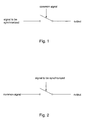
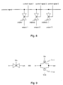
- FIG. 1 indicates the conventional method where the common signal is connected to the control electrode (gate terminal) of the transistor.
- the signal to be synchronized is connected to one of the input terminal and the output terminal of the transistor, and is output corresponding to the timing of the common signal.
- Fig. 2 shows a method of the present invention where the common signal is connected to one of the input terminal and the output terminal of the transistor.
- the signal to be synchronized is connected to the control electrode (gate terminal) of the transistor, the transistor is turned to an ON state by the signal to be synchronized, and a common signal is output in such a state.
- the transistor does not turn to an ON state due to the common signal, but the common signal is in continuity when the transistor is in an ON state.
- the transistor functions as a resistor in respect to the common signal, and is not easily influenced by a variation of the transistor.
- the MOS transistor and the MIS transistor are effected by the threshold during the time until the transistor is turned ON.
- the transistors were easily influenced by the variation of the threshold.
- the MOS transistor and the MIS transistor are transistors of controlling the electric conductive characteristic in which an electric field due to a voltage applied to a control electrode (gate terminal) is effected in a channel portion which is a current path between a source terminal and a drain terminal, corresponding to the input and output terminals.
- a signal as near as possible to the common signal may be obtained with this method.
- a buffer circuit was structured using a plurality of inverters.
- a common signal is passed through an analog switch, there is a merit that a buffer circuit becomes unnecessary. Note that, a plurality of common signals may exist in one electric circuit.
- a circuit for manufacturing a signal synchronized to a common signal by inputting a common signal into an input output terminal of a transistor is considered.
- Fig. 8 shows an example of a circuit having the same functions as an AND in Fig. 3 using an analog switch (shown as ASW).
- the analog switch is provided with a control terminal and an input terminal and output terminal in which a voltage applied to the control terminal determines the continuity or discontinuity.
- the control terminal is input with a control signal.
- a common signal is input one of the input terminal and the output terminal.
- Fig. 9 shows an example of a circuit structuring the analog switch using a MOS transistor.
- a capability balance is made by combining an n-channel MOS transistor 111 and a p-channel MOS transistor 112.
- the analog switch may function with only the n-channel MOS transistor or only the p-channel transistor.
- Vinb and Vin are opposite phase signals and are always output at an opposite phase logic level.
- the common signal is input to an input output electrode of the MOS transistor, and the control signal is input to a control electrode (gate terminal) of the MOS transistor.
- the transistor is turned to an ON state by the control signal, and then the common signal is input.
- the transistor is not turned ON by the common signal, but the common signal is in continuity when the transistor is in an ON state, so that the transistor functions as a resistor in respect to the common signal, and is not easily influenced by a variation of the transistor.
- the variation in the output signal is reduced compared with a case where the AND is used.
- a technique for manufacturing a thin film transistor (TFT) by forming a semiconductor thin film on a glass substrate is rapidly developing.
- the thin film transistors particularly a polycrystalline silicon thin film transistor (poly-Si TFT) may be operated at higher speed compared to an amorphous thin film transistor. Therefore, in a semiconductor display device using the polycrystalline silicon thin film transistor, different from the case where the amorphous thin film transistor is used, a driver circuit may be directly formed on the same substrate as a pixel portion.
- Fig. 10 shows a schematic view of one example.
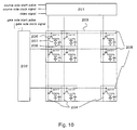
- a circuit diagram of the active matrix liquid crystal display device shown in Fig. 10 has a source side driver circuit 201, a gate side driver circuit 202 and a pixel portion 203.
- a source signal line 204 connected to the source side driver circuit 201, and a gate signal line 205 connected to the gate side driver circuit 202 intersect.
- a thin film transistor (pixel TFT) 206 of a pixel In the region provided (surrounded) with the source signal line 204 and the gate signal line 205, there are provided a thin film transistor (pixel TFT) 206 of a pixel, a liquid crystal cell 207 sandwiching a liquid crystal between an opposing electrode and a pixel electrode and a storage capacitor 208.
- pixel TFT thin film transistor
- An analog video signal output from the source side driver circuit 201 to the source signal line 204 (an analog video signal with image information) is selected by the pixel TFT 206, and written in a pixel electrode of the predetermined pixel.
- the pixel TFT 206 operates by the selected signal input from the gate side driver circuit 202 through the gate signal line 205.
- the circuit diagram of the active matrix liquid crystal display device shown in Fig. 10 has m ⁇ n pixels in the pixel portion 203. Namely, m source signal lines 204 and n gate signal lines 205 are necessary.
- the source side driver circuit 201 is input with a source side start pulse, a source side clock signal and a video signal, and the relationship of those is shown in Fig. 11.
- the start pulse shows the timing when the video signal starts, and the video signal transmits the image information for one pixel in the half cycle period of the clock.
- the information of the pixel in the first row to the pixel in the mth row sequentially aligns in the video signal.
- the source side driver circuit 201 is structured as shown in Fig. 12.
- SR1, SR2, ... , SR (m-1), and SR (m) are shift registers, and the state of the shift register immediately before is transmitted by the timing of the rise time of the clock and the fall time of the clock.
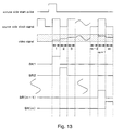
- Fig. 13 shows the output of SR1, SR2, ... , SR (m-1), and SR (m).
- the signals of the shift registers are sent to the analog switches ASW1, ASW2, ... , ASW (m-1) and ASW (m), and video signals are sent to the source signal line 204 at an appropriate timing.
- the source side clock signal refers to the "common signal” used in this specification. It is desirable that the variation in the output signal (sampling signal) of the shift register is suppressed as much as possible. This is because, when the timing in which the video signal is transmitted to the source signal line 204 varies, there is a possibility that an imaging failure, such as writing in a signal to be written to the next pixel, occurs.
- Fig. 14 shows an example of a conventional shift register circuit
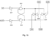
- Fig. 15 shows an example of a shift register circuit using the present invention
- Figs. 14 and 15 are examples of using an RS (set reset) flip flop as a shift register, and have the four input terminals SET, RESET, CLK (clock) for synchronization, and CLKb which has an opposite phase of CLK.
- the shift register circuit has as output terminals OUT and OUTb, where OUTb outputs an inverted signal of OUT.
- the output terminal OUT is connected to a SET terminal of a shift register in the next stage, and a control terminal of the analog switch connected to the source signal line 204 and a video signal, and the OUTb is connected to the RESET terminal of the shift register of the next level.
- Fig. 14 shows the RS flip-flop structured by an inverter 211, an inverter 212, a NAND 213 and a NAND 214.
- Fig. 15 shows the RS flip-flop structured by an inverter 221, an inverter 222, a NAND 223 and a NAND 214.
- Fig. 16 shows the structure of the inverter and Fig. 17 shows the structure of the NAND.
- the inverter shown in Fig. 16 is formed of a p-channel TFT 231 and an n-channel TFT 232, and outputs by inverting the input signal.
- the NAND shown in Fig. 17 is comprised of a p-channel TFT 233, a p-channel TFT 234, an n-channel TFT 235 and an n-channel TFT 236. Only in the case that Hi is input to the two input terminals, Low is output.
- Fig. 14 shows the example of the conventional circuit of the shift register, where a clocked inverter 215 and a clocked inverter 216 output the information of RS flip-flop in synchronization with the clock.
- Fig. 18 shows the structure of the clocked inverter.
- the clocked inverter is comprised of a p-channel TFT 237, a p-channel TFT 238, an n-channel TFT 239 and an n-channel TFT 240, and when CK is Hi and the inverted signal CKb of CK is Low, it operates as an inverter.
- Fig. 15 shows the example of the circuit of the shift register of the present invention, where the signal synchronized with the clock is output using an analog switch 225 and an analog switch 226.
- a signal with small variation may be output by changing a conventional clocked inverter to the analog switch.
- an output terminal OUT2 is formed by additionally providing an analog switch 246, and the OUT which outputs to the SET terminal of the shift register of the next stage and the OUT2 which outputs to the control terminal of the analog switch which is connected to the video signal and the source signal line 204 are separated from each other. Further, to ensure the logic operation, an n-channel TFT 249, an n-channel TFT 250 and a p-channel TFT 248 are provided.
- the gate side driver circuit 202 Up to here is the process of dividing the video signal by the source side driver circuit 201, and writing the divided video signals in the respective source signal lines 204.
- the gate side driver circuit 202 has selected one row of the gate signal line 205, the pixel TFT 206 of such row is turned ON, and the signal of the source signal line 204 is written into the liquid crystal cell 207 and the storage capacitor 208.
- the gate side driver circuit 202 needs to sequentially select the gate signal line 205, so similar to the source side driver circuit 201, the shift register is used to amplify the output of the shift register and to output to the gate signal line 205.
- the gate signal lines 205 are selected one by one. When all the gate signal lines are selected, one picture is formed.
- the present invention may be used for various semiconductor display devices.
- the present invention may be used in an active matrix liquid crystal display device, an active matrix EL display device (light emitting device), and an active matrix EC display device. That is, the present invention may be applied to all electric equipment combining the semiconductor device as a display medium.
- a video camera there are a digital camera, a projector (rear type or front type), a head mount display (goggle type display), a game machine, a car navigation system, a personal computer, a portable information terminal (a mobile computer, a portable telephone, an electronic book or the like). Examples of those are shown in Figs. 20A to 22C.
- Fig. 20A shows a personal computer which is structured by a main body 1001, an image input portion 1002, a display device 1003 and a keyboard 1004.
- the present invention may be applied to the display device 1003 and other circuits.
- registers refer to a register or the like which is a memory circuit that temporarily stores memory and digital data used as a storage medium.
- the register is a circuit which functions like a memo in the digital circuit.
- Fig. 20B shows a video camera which is structured by a main body 1101, a display device 1102, a voice input portion 1103, operating switches 1104, a battery 1105 and an image receiving portion 1106.
- the present invention may be applied to the display device 1102 and other circuits.
- Fig. 20C shows a mobile computer which is structured by a main body 1201, a camera portion 1202, an image receiving portion 1203, an operating switch 1204 and a display device 1205.
- the present invention may be applied to the display device 1205 and other circuits.
- Fig. 20D shows a goggle type display which is structured by a main body 1301, a display device 1302 and an arm portion 1303.
- the present invention may be applied to the display device 1302 and other circuits.
- Fig. 20E shows a player using a recording medium (hereafter referred to as recording medium) recorded with a program which is structured by a main body 1401, a display device 1402, speaker portions 1403, a recording medium 1404 and operating switches 1405.
- recording medium hereafter referred to as recording medium
- this device uses a DVD (digital versatile disc), CD or the like as a recording medium, and may be used to listen to music, to see a movie, to play games and to use the Internet.
- the present invention may be applied to the display device 1402 and other circuits.
- Fig. 21A is a front type projector which is structured by a light source optical system and a display device 1601, and a screen 1602.
- the present invention may be applied to the display device 1601 and other circuits.
- Fig. 21B is a rear type projector which is structured by a main body 1701, a light source optical system and a display device 1702, a mirror 1703, a mirror 1704 and a screen 1705.
- the present invention may be applied to the display device 1702 and other circuits.
- Fig. 21C is a diagram showing an example of a structure of the light source optical system and the display device 1601 or 1702 in Fig. 21A or 21B.
- the light source optical system and the display device 1601, 1702 are structured by a light source optical system 1801, mirrors 1802, 1804 to 1806, a dichroic mirror 1803, an optical system 1807, a display device 1808, a phase difference plate 1809 and a projection optical system 1810.
- the projection optical system 1810 is structured by a plurality of optical lenses provided with a projection lens. This structure is referred to as a three-plate system since it uses three display devices 1808. Further, the operator may provide in the optical path shown by an arrow in Fig. 21C, an optical lens, a film having polarizing functions, a film for adjusting the phase difference, an IR film and the like.
- Fig. 21D shows a diagram showing an example of a structure of the light source optical system 1801 in Fig. 21C.
- the light source optical system 1801 is structured by a reflector 1811, a light source 1812, lens arrays 1813 and 1814, a polarizing conversion element 1815 and a condenser lens 1816.
- the light source optical system shown in Fig. 21D is one example, and it is not limited to this structure.
- the operator may appropriately provide a light source lens, a film having polarizing functions, a film for adjusting the phase difference, an IR film and the like.
- Fig. 21C shows an example of a three-plate system
- Fig. 22A is a diagram showing an example of a single-plate system.
- the light source optical system and the display device shown in Fig. 22A is structured by a light source optical system 1901, a display device 1902, a projection optical system 1903 and a phase difference plate 1904.
- the projection optical system 1903 is structured by a plurality of optical lenses with a projection lens.
- the light source optical system and the display device shown in Fig. 22A may be applied to the light source optical systems and the display devices 1601, 1702 in Figs. 21A and 21B.
- the light source optical system 1901 may use the light source optical system shown in Fig. 21D.
- the display device 1902 is provided with a color filter (not shown), and displays images in color.
- the light source optical system and the display device shown in Fig. 22B is an applied example of Fig. 22A, and instead of providing a color filter, a RGB rotating color filter disk 1905 is used to display images in color.
- the light source optical system and the display device shown in Fig. 22B may be applied to the light source optical systems and the display devices 1601, 1702 shown in Figs. 21A and 21B.
- the light source optical system and the display device shown in Fig. 22C is referred to as a color-filterless single-plate system.
- This system provides a micro lens array 1915 in the display device 1916 and displays a color image by using a dichroic mirror (green) 1912, a dichroic mirror (red) 1913 and a dichroic mirror (blue) 1914.
- a projection optical system 1917 is structured by a plurality of optical lenses provided with projection lenses.
- the light source optical system and the display device shown in Fig. 22C may be applied to the light source optical systems and the display devices 1601, 1702 shown in Figs. 21A and 21B.
- a light source optical system 1911 an optical system using a coupling lens and a collimator lens in addition to the light source may be used.
- the application range of the present invention is extremely wide and the present invention may be applied to various fields of electronic equipment.
- the structure of the present invention is simple, and may be applied to all semiconductor circuits to be operated with synchronization. Further, an effect of reducing the shift from the synchronized signal due to the variation of the semiconductor element may be expected.
Landscapes
- Engineering & Computer Science (AREA)
- Theoretical Computer Science (AREA)
- Physics & Mathematics (AREA)
- Crystallography & Structural Chemistry (AREA)
- Computer Hardware Design (AREA)
- General Physics & Mathematics (AREA)
- Chemical & Material Sciences (AREA)
- Control Of Indicators Other Than Cathode Ray Tubes (AREA)
- Liquid Crystal Display Device Control (AREA)
- Logic Circuits (AREA)
- Transforming Electric Information Into Light Information (AREA)
- Electronic Switches (AREA)
- Analogue/Digital Conversion (AREA)
Abstract
Description
Claims (22)
- A driving method of an electronic circuit having an analog switch, wherein the analog switch synchronizes with a signal input to the electronic circuit, and samples a common signal input to the analog switch to output it.
- A driving method of an electronic circuit having an analog switch, wherein the analog switch synchronizes with a video signal input to the electronic circuit, and samples a common signal input to the analog switch to output it.
- A driving method of an electronic circuit according to claim 1, wherein the common signal is a clock signal or a clock back signal.
- A driving method of an electronic circuit according to claim 2, wherein the common signal is a clock signal or a clock back signal.
- A driving method of an electronic circuit according to claim 1, wherein the common signal is a trigger signal.
- A driving method of an electronic circuit according to claim 2, wherein the common signal is a trigger signal.
- A driving method of an electronic circuit according to claim 1, wherein the analog switch comprises a MOS transistor or a MIS transistor.
- A driving method of an electronic circuit according to claim 2, wherein the analog switch comprises a MOS transistor or a MIS transistor.
- A driving method of an electronic circuit comprising a flip-flop, a first analog switch and a second analog switch, wherein:a first signal and a second signal are output from the flip-flop;the first analog signal synchronizes with a third signal input to the electric circuit, and samples the first common signal input to the analog switch to output it; andthe second analog switch synchronizes with a fourth signal input to the electric circuit, samples the second common signal input to the analog switch to output it.
- A driving method of an electronic circuit according to claim 9, wherein the first signal and the second signal are always output at an opposite logic level.
- A driving method of an electronic circuit according to claim 9, wherein the third signal and the fourth signal are video signals.
- A driving method of an electronic circuit according to claim 9, wherein the first analog switch and the second analog switch comprise a MOS transistor or a MIS transistor.
- A driving method of an electronic circuit according to claim 9, wherein out of the first common signal and the second common signal, one is a clock signal, and the other is a clock back signal.
- A driving method of an electronic circuit according to claim 9, wherein the first common signal and the second common signal are trigger signals.
- A driving method of an electronic circuit wherein the electronic circuit as claimed in claims 1 is a digital circuit.
- A driving method of an electronic circuit wherein the electronic circuit as claimed in claims 2 is a digital circuit.
- A driving method of an electronic circuit wherein the electronic circuit as claimed in claims 9 is a digital circuit.
- A driving method of an electronic circuit as claimed in claim 1, wherein said method is used in a device selected from the group of: an image display device, a light emitting device, a liquid crystal display device, a memory, a register and electronic equipment.
- A driving method of an electronic circuit as claimed in claim 2, wherein said method is used in a device selected from the group of: an image display device, a light emitting device, a liquid crystal display device, a memory, a register and electronic equipment.
- A driving method of an electronic circuit as claimed in claim 9, wherein said method is used in a device selected from the group of: an image display device, a light emitting device, a liquid crystal display device, a memory, a register and electronic equipment.
- A driving method of a display device comprising:at least one driver circuit having at least one shift register comprising at least one first analog switch, said first analog switch having a first control terminal, a first input terminal and a first output terminal;at least one second analog switch electrically connected to said shift register, said second analog switch having a first control terminal electrically connected to said first output terminal, a second input terminal and a second output terminal; andat least one pixel electrically connected to said output terminal, said method comprising the steps of:inputting a start pulse to said shift register;inputting a first signal to said first control terminal in response to said start pulse;inputting a clock signal to said first input terminal after inputting said first signal;outputting a second signal from said first output terminal;inputting said second signal to said second control terminal;inputting a video signal to said second input terminal;outputting a video signal in synchronization with said second signal to said pixel.
- A driving method of an display device as claimed in claim 21, wherein said method is used in a device selected from the group of: an image display device, a light emitting device, a liquid crystal display device.
Applications Claiming Priority (2)
| Application Number | Priority Date | Filing Date | Title |
|---|---|---|---|
| JP2000232450 | 2000-07-31 | ||
| JP2000232450 | 2000-07-31 |
Publications (3)
| Publication Number | Publication Date |
|---|---|
| EP1178607A2 true EP1178607A2 (en) | 2002-02-06 |
| EP1178607A3 EP1178607A3 (en) | 2004-12-01 |
| EP1178607B1 EP1178607B1 (en) | 2010-05-26 |
Family
ID=18725134
Family Applications (1)
| Application Number | Title | Priority Date | Filing Date |
|---|---|---|---|
| EP01118348A Expired - Lifetime EP1178607B1 (en) | 2000-07-31 | 2001-07-27 | Driving method of an electric circuit |
Country Status (7)
| Country | Link |
|---|---|
| US (5) | US7164414B2 (en) |
| EP (1) | EP1178607B1 (en) |
| JP (1) | JP4519372B2 (en) |
| KR (2) | KR100823046B1 (en) |
| CN (2) | CN1340918B (en) |
| DE (1) | DE60142209D1 (en) |
| TW (1) | TWI237802B (en) |
Cited By (1)
| Publication number | Priority date | Publication date | Assignee | Title |
|---|---|---|---|---|
| EP1826741A3 (en) * | 2006-02-23 | 2012-02-15 | Semiconductor Energy Laboratory Co., Ltd. | Display device and electronic device having the same |
Families Citing this family (36)
| Publication number | Priority date | Publication date | Assignee | Title |
|---|---|---|---|---|
| TWI237802B (en) * | 2000-07-31 | 2005-08-11 | Semiconductor Energy Lab | Driving method of an electric circuit |
| US11302253B2 (en) | 2001-09-07 | 2022-04-12 | Joled Inc. | El display apparatus |
| US8823606B2 (en) * | 2001-09-07 | 2014-09-02 | Panasonic Corporation | EL display panel, its driving method, and EL display apparatus |
| TWI263191B (en) * | 2003-11-18 | 2006-10-01 | Ind Tech Res Inst | Shift-register circuit |
| US8576217B2 (en) | 2011-05-20 | 2013-11-05 | Ignis Innovation Inc. | System and methods for extraction of threshold and mobility parameters in AMOLED displays |
| US10013907B2 (en) | 2004-12-15 | 2018-07-03 | Ignis Innovation Inc. | Method and system for programming, calibrating and/or compensating, and driving an LED display |
| US9799246B2 (en) | 2011-05-20 | 2017-10-24 | Ignis Innovation Inc. | System and methods for extraction of threshold and mobility parameters in AMOLED displays |
| EP1717783B1 (en) * | 2005-04-28 | 2015-06-03 | Semiconductor Energy Laboratory Co., Ltd. | Data latch circuit, driving method of the data latch circuit, and display device |
| US7852298B2 (en) | 2005-06-08 | 2010-12-14 | Ignis Innovation Inc. | Method and system for driving a light emitting device display |
| EP2008264B1 (en) | 2006-04-19 | 2016-11-16 | Ignis Innovation Inc. | Stable driving scheme for active matrix displays |
| JP5374879B2 (en) * | 2008-01-28 | 2013-12-25 | セイコーエプソン株式会社 | Output circuit and electronic equipment |
| US10319307B2 (en) | 2009-06-16 | 2019-06-11 | Ignis Innovation Inc. | Display system with compensation techniques and/or shared level resources |
| US9384698B2 (en) | 2009-11-30 | 2016-07-05 | Ignis Innovation Inc. | System and methods for aging compensation in AMOLED displays |
| US9311859B2 (en) | 2009-11-30 | 2016-04-12 | Ignis Innovation Inc. | Resetting cycle for aging compensation in AMOLED displays |
| CN107195328B (en) | 2009-10-09 | 2020-11-10 | 株式会社半导体能源研究所 | Shift register, display device and method of driving the same |
| US10089921B2 (en) | 2010-02-04 | 2018-10-02 | Ignis Innovation Inc. | System and methods for extracting correlation curves for an organic light emitting device |
| US20140313111A1 (en) | 2010-02-04 | 2014-10-23 | Ignis Innovation Inc. | System and methods for extracting correlation curves for an organic light emitting device |
| CA2692097A1 (en) | 2010-02-04 | 2011-08-04 | Ignis Innovation Inc. | Extracting correlation curves for light emitting device |
| US9881532B2 (en) | 2010-02-04 | 2018-01-30 | Ignis Innovation Inc. | System and method for extracting correlation curves for an organic light emitting device |
| US9530349B2 (en) | 2011-05-20 | 2016-12-27 | Ignis Innovations Inc. | Charged-based compensation and parameter extraction in AMOLED displays |
| US9466240B2 (en) | 2011-05-26 | 2016-10-11 | Ignis Innovation Inc. | Adaptive feedback system for compensating for aging pixel areas with enhanced estimation speed |
| JP2014517940A (en) | 2011-05-27 | 2014-07-24 | イグニス・イノベイション・インコーポレーテッド | System and method for aging compensation in AMOLED displays |
| US10089924B2 (en) | 2011-11-29 | 2018-10-02 | Ignis Innovation Inc. | Structural and low-frequency non-uniformity compensation |
| US9324268B2 (en) | 2013-03-15 | 2016-04-26 | Ignis Innovation Inc. | Amoled displays with multiple readout circuits |
| US8937632B2 (en) | 2012-02-03 | 2015-01-20 | Ignis Innovation Inc. | Driving system for active-matrix displays |
| CN103297016B (en) * | 2012-03-01 | 2020-06-19 | 朗美通技术英国有限公司 | Optical transmitter and optical communication method |
| US8922544B2 (en) | 2012-05-23 | 2014-12-30 | Ignis Innovation Inc. | Display systems with compensation for line propagation delay |
| EP2779147B1 (en) | 2013-03-14 | 2016-03-02 | Ignis Innovation Inc. | Re-interpolation with edge detection for extracting an aging pattern for AMOLED displays |
| US9761170B2 (en) | 2013-12-06 | 2017-09-12 | Ignis Innovation Inc. | Correction for localized phenomena in an image array |
| US9502653B2 (en) | 2013-12-25 | 2016-11-22 | Ignis Innovation Inc. | Electrode contacts |
| CN103928001B (en) | 2013-12-31 | 2016-12-07 | 上海天马微电子有限公司 | Grid driving circuit and display device |
| CA2879462A1 (en) | 2015-01-23 | 2016-07-23 | Ignis Innovation Inc. | Compensation for color variation in emissive devices |
| CA2889870A1 (en) | 2015-05-04 | 2016-11-04 | Ignis Innovation Inc. | Optical feedback system |
| CA2892714A1 (en) | 2015-05-27 | 2016-11-27 | Ignis Innovation Inc | Memory bandwidth reduction in compensation system |
| CA2900170A1 (en) | 2015-08-07 | 2017-02-07 | Gholamreza Chaji | Calibration of pixel based on improved reference values |
| CN108540117A (en) * | 2018-03-14 | 2018-09-14 | 湖北楚航电子科技有限公司 | A kind of high power PIN RF switch driving circuits |
Family Cites Families (31)
| Publication number | Priority date | Publication date | Assignee | Title |
|---|---|---|---|---|
| AU588062B2 (en) * | 1985-10-16 | 1989-09-07 | Sanyo Electric Co., Ltd. | Lcd matrix alternating drive circuit |
| US4845482A (en) * | 1987-10-30 | 1989-07-04 | International Business Machines Corporation | Method for eliminating crosstalk in a thin film transistor/liquid crystal display |
| US4980583A (en) * | 1989-01-03 | 1990-12-25 | National Semiconductor Corporation | CMOS level shift circuit with active pull-up and pull-down |
| JPH03148695A (en) | 1989-07-28 | 1991-06-25 | Hitachi Ltd | liquid crystal display device |
| JPH03147598A (en) * | 1989-11-02 | 1991-06-24 | Sony Corp | Shift register |
| JPH04136981A (en) * | 1990-09-28 | 1992-05-11 | Sharp Corp | Driver circuit for display device |
| US5849601A (en) | 1990-12-25 | 1998-12-15 | Semiconductor Energy Laboratory Co., Ltd. | Electro-optical device and method for manufacturing the same |
| JPH0652689A (en) | 1992-07-29 | 1994-02-25 | Sony Corp | Memory device |
| JPH07236148A (en) | 1994-02-23 | 1995-09-05 | Asahi Optical Co Ltd | Pixel signal generator |
| CN1136529C (en) | 1994-05-31 | 2004-01-28 | 夏普株式会社 | Sampling circuit, signal amplifier, and image display |
| JPH086523A (en) * | 1994-06-21 | 1996-01-12 | Sharp Corp | Sampling circuit and image display device |
| JPH08211854A (en) * | 1994-11-29 | 1996-08-20 | Sanyo Electric Co Ltd | Driver circuit for display device, and display device |
| JP2715943B2 (en) | 1994-12-02 | 1998-02-18 | 日本電気株式会社 | Drive circuit for liquid crystal display |
| CN100576306C (en) * | 1995-02-01 | 2009-12-30 | 精工爱普生株式会社 | Liquid crystal display device |
| JPH09166771A (en) | 1995-12-18 | 1997-06-24 | Seiko Epson Corp | Power supply circuit |
| JP3516323B2 (en) * | 1996-05-23 | 2004-04-05 | シャープ株式会社 | Shift register circuit and image display device |
| JPH09320284A (en) * | 1996-05-31 | 1997-12-12 | Nec Corp | Semiconductor integrated circuit and setting method for state of terminal |
| JP3062110B2 (en) | 1997-02-27 | 2000-07-10 | 日本電気アイシーマイコンシステム株式会社 | Data latch circuit |
| JP3675113B2 (en) | 1997-06-10 | 2005-07-27 | ソニー株式会社 | Display device |
| JPH11161243A (en) * | 1997-09-26 | 1999-06-18 | Sharp Corp | Liquid crystal display |
| US6392573B1 (en) * | 1997-12-31 | 2002-05-21 | Intel Corporation | Method and apparatus for reduced glitch energy in digital-to-analog converter |
| KR20000019416A (en) | 1998-09-11 | 2000-04-06 | 김영남 | Gate driving circuit for field emission display |
| JP2000200072A (en) | 1998-11-04 | 2000-07-18 | Matsushita Electric Ind Co Ltd | Operation circuit and built-in drive circuit of liquid crystal display panel using the operation circuit |
| JP3339438B2 (en) | 1998-12-15 | 2002-10-28 | 日本電気株式会社 | Display device and method |
| JP3374820B2 (en) * | 1999-01-08 | 2003-02-10 | セイコーエプソン株式会社 | Output buffer circuit |
| JP3473745B2 (en) * | 1999-05-28 | 2003-12-08 | シャープ株式会社 | Shift register and image display device using the same |
| JP2001051303A (en) * | 1999-08-05 | 2001-02-23 | Fujitsu Ltd | Liquid crystal display device and method of manufacturing the same |
| US7285653B1 (en) | 1999-08-27 | 2007-10-23 | Bayer Aktiengesellschaft | Nucleic acids which code for the enzyme activities of the spinosyn biosynthesis |
| JP2001109436A (en) * | 1999-10-08 | 2001-04-20 | Oki Electric Ind Co Ltd | Matrix type display device |
| JP3326691B2 (en) | 2000-07-18 | 2002-09-24 | ソニー株式会社 | display |
| TWI237802B (en) * | 2000-07-31 | 2005-08-11 | Semiconductor Energy Lab | Driving method of an electric circuit |
-
2001
- 2001-07-12 TW TW090117124A patent/TWI237802B/en not_active IP Right Cessation
- 2001-07-18 US US09/906,617 patent/US7164414B2/en not_active Expired - Fee Related
- 2001-07-25 JP JP2001224439A patent/JP4519372B2/en not_active Expired - Lifetime
- 2001-07-27 EP EP01118348A patent/EP1178607B1/en not_active Expired - Lifetime
- 2001-07-27 DE DE60142209T patent/DE60142209D1/en not_active Expired - Lifetime
- 2001-07-30 KR KR1020010045865A patent/KR100823046B1/en not_active Expired - Fee Related
- 2001-07-31 CN CN011247509A patent/CN1340918B/en not_active Expired - Fee Related
- 2001-07-31 CN CN2010101562671A patent/CN101847984B/en not_active Expired - Lifetime
-
2006
- 2006-02-02 US US11/275,905 patent/US7358763B2/en not_active Expired - Lifetime
- 2006-06-12 KR KR1020060052521A patent/KR100756210B1/en not_active Expired - Lifetime
-
2008
- 2008-04-02 US US12/061,201 patent/US8232982B2/en not_active Expired - Fee Related
-
2012
- 2012-07-23 US US13/555,226 patent/US8421783B2/en not_active Expired - Fee Related
-
2013
- 2013-04-15 US US13/862,539 patent/US9153187B2/en not_active Expired - Fee Related
Cited By (2)
| Publication number | Priority date | Publication date | Assignee | Title |
|---|---|---|---|---|
| EP1826741A3 (en) * | 2006-02-23 | 2012-02-15 | Semiconductor Energy Laboratory Co., Ltd. | Display device and electronic device having the same |
| US8223104B2 (en) | 2006-02-23 | 2012-07-17 | Semiconductor Energy Laboratory Co., Ltd. | Display device and electronic device having the same |
Also Published As
| Publication number | Publication date |
|---|---|
| EP1178607A3 (en) | 2004-12-01 |
| KR100823046B1 (en) | 2008-04-18 |
| US20130241813A1 (en) | 2013-09-19 |
| JP2002176345A (en) | 2002-06-21 |
| US20120287096A1 (en) | 2012-11-15 |
| US8232982B2 (en) | 2012-07-31 |
| JP4519372B2 (en) | 2010-08-04 |
| DE60142209D1 (en) | 2010-07-08 |
| US20080191988A1 (en) | 2008-08-14 |
| US7358763B2 (en) | 2008-04-15 |
| US7164414B2 (en) | 2007-01-16 |
| CN101847984A (en) | 2010-09-29 |
| TWI237802B (en) | 2005-08-11 |
| US9153187B2 (en) | 2015-10-06 |
| US8421783B2 (en) | 2013-04-16 |
| CN1340918A (en) | 2002-03-20 |
| KR20060089684A (en) | 2006-08-09 |
| US20060125525A1 (en) | 2006-06-15 |
| KR100756210B1 (en) | 2007-09-07 |
| CN1340918B (en) | 2010-05-26 |
| KR20020011103A (en) | 2002-02-07 |
| EP1178607B1 (en) | 2010-05-26 |
| US20020013018A1 (en) | 2002-01-31 |
| CN101847984B (en) | 2012-09-05 |
Similar Documents
| Publication | Publication Date | Title |
|---|---|---|
| US9153187B2 (en) | Driving method of an electric circuit | |
| US10916319B2 (en) | Pulse output circuit, shift register and display device | |
| US7268756B2 (en) | Liquid crystal display device and method of driving a liquid crystal display device | |
| US7133017B2 (en) | Shift register and display device using same | |
| KR100991684B1 (en) | Liquid crystal display device and method of driving a liquid crystal display device | |
| US8264254B2 (en) | Clocked inverter, NAND, NOR and shift register | |
| JP6248268B2 (en) | Image display device | |
| WO2020155920A1 (en) | Shift register and driving method thereof, gate driving circuit, and display device | |
| JP4637467B2 (en) | Liquid crystal display device and driving method of liquid crystal display device | |
| CN101221732B (en) | A system that uses a horizontal offset register to generate a repetitive output signal to display an image | |
| JP4707858B2 (en) | Shift register, display device using the same, camera system, and portable terminal device | |
| US7088165B2 (en) | Voltage level shifter and sequential pulse generator |
Legal Events
| Date | Code | Title | Description |
|---|---|---|---|
| PUAI | Public reference made under article 153(3) epc to a published international application that has entered the european phase |
Free format text: ORIGINAL CODE: 0009012 |
|
| AK | Designated contracting states |
Kind code of ref document: A2 Designated state(s): AT BE CH CY DE DK ES FI FR GB GR IE IT LI LU MC NL PT SE TR |
|
| AX | Request for extension of the european patent |
Free format text: AL;LT;LV;MK;RO;SI |
|
| PUAL | Search report despatched |
Free format text: ORIGINAL CODE: 0009013 |
|
| AK | Designated contracting states |
Kind code of ref document: A3 Designated state(s): AT BE CH CY DE DK ES FI FR GB GR IE IT LI LU MC NL PT SE TR |
|
| AX | Request for extension of the european patent |
Extension state: AL LT LV MK RO SI |
|
| RIC1 | Information provided on ipc code assigned before grant |
Ipc: 7H 03K 17/687 A Ipc: 7G 09G 3/36 B |
|
| 17P | Request for examination filed |
Effective date: 20050531 |
|
| AKX | Designation fees paid |
Designated state(s): DE FI FR GB NL |
|
| GRAP | Despatch of communication of intention to grant a patent |
Free format text: ORIGINAL CODE: EPIDOSNIGR1 |
|
| GRAS | Grant fee paid |
Free format text: ORIGINAL CODE: EPIDOSNIGR3 |
|
| GRAA | (expected) grant |
Free format text: ORIGINAL CODE: 0009210 |
|
| AK | Designated contracting states |
Kind code of ref document: B1 Designated state(s): DE FI FR GB NL |
|
| REG | Reference to a national code |
Ref country code: GB Ref legal event code: FG4D |
|
| REF | Corresponds to: |
Ref document number: 60142209 Country of ref document: DE Date of ref document: 20100708 Kind code of ref document: P |
|
| REG | Reference to a national code |
Ref country code: NL Ref legal event code: VDEP Effective date: 20100526 |
|
| PG25 | Lapsed in a contracting state [announced via postgrant information from national office to epo] |
Ref country code: FI Free format text: LAPSE BECAUSE OF FAILURE TO SUBMIT A TRANSLATION OF THE DESCRIPTION OR TO PAY THE FEE WITHIN THE PRESCRIBED TIME-LIMIT Effective date: 20100526 |
|
| PG25 | Lapsed in a contracting state [announced via postgrant information from national office to epo] |
Ref country code: NL Free format text: LAPSE BECAUSE OF FAILURE TO SUBMIT A TRANSLATION OF THE DESCRIPTION OR TO PAY THE FEE WITHIN THE PRESCRIBED TIME-LIMIT Effective date: 20100526 |
|
| PLBE | No opposition filed within time limit |
Free format text: ORIGINAL CODE: 0009261 |
|
| STAA | Information on the status of an ep patent application or granted ep patent |
Free format text: STATUS: NO OPPOSITION FILED WITHIN TIME LIMIT |
|
| 26N | No opposition filed |
Effective date: 20110301 |
|
| REG | Reference to a national code |
Ref country code: DE Ref legal event code: R097 Ref document number: 60142209 Country of ref document: DE Effective date: 20110228 |
|
| PGFP | Annual fee paid to national office [announced via postgrant information from national office to epo] |
Ref country code: GB Payment date: 20120725 Year of fee payment: 12 |
|
| PGFP | Annual fee paid to national office [announced via postgrant information from national office to epo] |
Ref country code: FR Payment date: 20120719 Year of fee payment: 12 |
|
| GBPC | Gb: european patent ceased through non-payment of renewal fee |
Effective date: 20130727 |
|
| REG | Reference to a national code |
Ref country code: FR Ref legal event code: ST Effective date: 20140331 |
|
| PG25 | Lapsed in a contracting state [announced via postgrant information from national office to epo] |
Ref country code: GB Free format text: LAPSE BECAUSE OF NON-PAYMENT OF DUE FEES Effective date: 20130727 |
|
| PG25 | Lapsed in a contracting state [announced via postgrant information from national office to epo] |
Ref country code: FR Free format text: LAPSE BECAUSE OF NON-PAYMENT OF DUE FEES Effective date: 20130731 |
|
| PGFP | Annual fee paid to national office [announced via postgrant information from national office to epo] |
Ref country code: DE Payment date: 20170719 Year of fee payment: 17 |
|
| REG | Reference to a national code |
Ref country code: DE Ref legal event code: R119 Ref document number: 60142209 Country of ref document: DE |
|
| PG25 | Lapsed in a contracting state [announced via postgrant information from national office to epo] |
Ref country code: DE Free format text: LAPSE BECAUSE OF NON-PAYMENT OF DUE FEES Effective date: 20190201 |