EP1176667A2 - Slot antenna with a conductive box structure - Google Patents
Slot antenna with a conductive box structure Download PDFInfo
- Publication number
- EP1176667A2 EP1176667A2 EP01305819A EP01305819A EP1176667A2 EP 1176667 A2 EP1176667 A2 EP 1176667A2 EP 01305819 A EP01305819 A EP 01305819A EP 01305819 A EP01305819 A EP 01305819A EP 1176667 A2 EP1176667 A2 EP 1176667A2
- Authority
- EP
- European Patent Office
- Prior art keywords
- conductive
- slot
- antenna
- ground plane
- plane
- Prior art date
- Legal status (The legal status is an assumption and is not a legal conclusion. Google has not performed a legal analysis and makes no representation as to the accuracy of the status listed.)
- Withdrawn
Links
- 239000000758 substrate Substances 0.000 claims abstract description 24
- 230000005855 radiation Effects 0.000 claims description 12
- 238000005516 engineering process Methods 0.000 abstract description 3
- 239000011248 coating agent Substances 0.000 abstract 1
- 238000000576 coating method Methods 0.000 abstract 1
- 239000004020 conductor Substances 0.000 description 6
- 230000005404 monopole Effects 0.000 description 4
- 239000011324 bead Substances 0.000 description 3
- 238000010276 construction Methods 0.000 description 3
- 230000000694 effects Effects 0.000 description 3
- 229910000679 solder Inorganic materials 0.000 description 3
- 238000009434 installation Methods 0.000 description 2
- 239000000463 material Substances 0.000 description 2
- 238000000034 method Methods 0.000 description 2
- 230000005540 biological transmission Effects 0.000 description 1
- 238000004590 computer program Methods 0.000 description 1
- 230000005672 electromagnetic field Effects 0.000 description 1
- 239000012212 insulator Substances 0.000 description 1
- 238000004519 manufacturing process Methods 0.000 description 1
- 238000004088 simulation Methods 0.000 description 1
Images



Classifications
-
- H—ELECTRICITY
- H01—ELECTRIC ELEMENTS
- H01Q—ANTENNAS, i.e. RADIO AERIALS
- H01Q1/00—Details of, or arrangements associated with, antennas
- H01Q1/36—Structural form of radiating elements, e.g. cone, spiral, umbrella; Particular materials used therewith
- H01Q1/38—Structural form of radiating elements, e.g. cone, spiral, umbrella; Particular materials used therewith formed by a conductive layer on an insulating support
-
- H—ELECTRICITY
- H01—ELECTRIC ELEMENTS
- H01Q—ANTENNAS, i.e. RADIO AERIALS
- H01Q13/00—Waveguide horns or mouths; Slot antennas; Leaky-waveguide antennas; Equivalent structures causing radiation along the transmission path of a guided wave
- H01Q13/10—Resonant slot antennas
- H01Q13/18—Resonant slot antennas the slot being backed by, or formed in boundary wall of, a resonant cavity ; Open cavity antennas
-
- H—ELECTRICITY
- H01—ELECTRIC ELEMENTS
- H01Q—ANTENNAS, i.e. RADIO AERIALS
- H01Q23/00—Antennas with active circuits or circuit elements integrated within them or attached to them
Definitions
- the present invention relates to antennas, and more particularly relates to a boxed-in slot antenna.
- WLANs may operate under a number of standards, for example, the so-called “Bluetooth” standard.
- Bluetooth radio frequency
- FIG. 1 shows a prior art slot antenna 10.
- a conductive ground plane 12, typically metallic, is formed with a slot 14.
- the slot has a length, L, which is typically equal to half of the electric wavelength ⁇ e .
- the slot 14 typically also has a width, w, which is much less than the wavelength.
- Such an antenna will radiate equally from both sides of the ground plane 12. It is typically fed by a coaxial cable 16, which can be attached at an off-centre feed point in order to obtain a 50 Ohm antenna impedance so as to match the characteristic impedance, typically 50 Ohms, of coaxial cables.
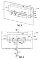
- FIG. 3 shows one embodiment of boxed-in slot antenna 100 for radiation having a free-space wavelength ⁇ , a waveguide wavelength ⁇ g , and an electric half-wavelength ⁇ e /2, in accordance with the present invention.
- the antenna 100 includes a conductive ground plane 102, which can be metallic (for example), and which has a slot 104 formed therein.
- Ground plane 102 has first and second sides.
- the slot 104 has a length L which is at least substantially equal to the electric half-wavelength.
- "at least substantially equal to” means that L is greater than the electric half-wavelength, or is substantially equal to the electric half-wavelength, where substantially equal is meant to include equal to, or slightly greater than or less than, so long as functionality can be maintained.
- Slot 104 also has a width w which is less (preferably much less) than the length L, and further has a longitudinal axis 106 and first and second longitudinal edges 108, 110 respectively. It is preferable that the width w satisfy the relationship w ⁇ . Slot 104 can be configured and dimensioned for predetermined radiation performance, for example, for radiation as described above. Those of skill in the antenna art will appreciate how to develop desired dimensions for the slot in view of the guidelines presented herein.
- the distance d should be as thin as possible to reduce size, consistent with adequate bandwidth. If d is too small, the bandwidth will be narrow. Appropriate values for d will also be influenced by the properties of the substrate in PCB embodiments of the invention to be discussed below. Any value of the distance d which is substantially less than 1 ⁇ 4 of the waveguide wavelength should be considered within the scope of the invention. For example, d could be less than 15% of ⁇ g , or preferably less than 10% of ⁇ g , or even more preferably less than 5% of ⁇ g , consistent with adequate bandwidth. In the Example discussed below, d is about 3.8% of ⁇ g . In view of these guidelines, those of skill in the antenna art will be able to select appropriate values for the distance d.
- Conductive box structure 112 further comprises first and second conductive structures 116, 118 respectively, which are substantially parallel to each other and which are spaced apart a distance g which is at least substantially equal to L (i.e., either substantially equal to L or greater than L). It is preferable that g be at least slightly greater than L.
- the first and second conductive structures 116, 118 are substantially perpendicular to the conductive ground plane 102 and to the main conductive plane 114, and are also substantially perpendicular to the longitudinal axis of the slot 106.
- a "plan” view refers to a view wherein the conductive ground plane is parallel to the paper on which the view is drawn. Furthermore, “bounding" of the slot by the conductive structures refers to the structures surrounding, or being substantially coincident with, the slot.
- the distance a is substantially equal to the width w plus 1 ⁇ 4 of the waveguide wavelength ⁇ g .
- the third conductive structure 120 can, as shown, substantially coincide with the first longitudinal edge 108 of the slot 104. "Substantially coinciding" is intended to refer to a spatial orientation wherein the third conductive structure 120 is even with or only slightly displaced from the first longitudinal edge 108 of the slot 104.
- the fourth conductive structure 122 in the embodiment depicted in FIG. 3, can be located beyond the second longitudinal edge 110 of the slot 104, spaced from the third conductive structure 120 in a direction moving from the first longitudinal edge 108 of the slot 104 to the second longitudinal edge 110 of the slot 104.
- Outer conductor 230 of coaxial cable 224 can be soldered to first longitudinal edge 208 of slot 204 through a solder bead 232, while centre conductor 226 of coaxial cable 224 can be soldered to second longitudinal edge 210 of slot 204 at a solder bead 234. While the outer conductor 230 of coaxial cable 224 is shown as being spaced from conductive ground plane 202, with conductive contact only at solder bead 232, it should be appreciated that the outer conductor 230 can be maintained in contact with the conductive ground plane 202 if desired (such contact may be advantageous).
- FIGS. 6 and 7 depict an embodiment of the invention similar to that shown in FIG. 3, which employs printed circuit board (PCB) technology. Items in FIGS. 6 and 7 which are similar to those in FIGS. 4 and 5 have received the same reference character incremented by 100.
- the embodiment of FIGS. 6 and 7 is designated generally as 300, and can include a first printed circuit board substrate 336 having first and second generally planar surfaces 338, 340 respectively.
- the conductive ground plane 302 can be formed as a first conductive layer 342 which is deposited on the first generally planar surface 338 of the first PCB substrate 336.
- the slot 304 can be etched in the first conductive layer 342.
- the main conductive plane 314 can be formed as a second conductive layer 344 which is deposited on the second generally planar surface 340 of the first PCB substrate 336.
- the first, second, third and fourth conductive structures 316, 318, 320, 322 respectively can each be formed as a series of plated through holes 346 which are formed in the first PCB substrate 336 using techniques well known in the art of printed circuit board fabrication. It will be appreciated that the plated through holes 346 provide an electrically conductive path between the first and second conductive layers 342, 344. As best seen in FIG. 6, the plated through holes 346 which form the conductive structures can be spaced apart by a distance ⁇ , which is preferably no more than substantially one tenth of the free-space wavelength ⁇ .
- the foregoing terminology is meant to cover plated through holes which are spaced slightly more than one tenth of ⁇ apart, but which are still functional, and any closer spacing of the through holes 346.
- the second conductive layer 344 can extend over the entire second surface 340 of the first PCB substrate 336, or, if desired, can extend only over the region where it serves as the main conductive plane 314, that is, within the region defined by the plated through holes 346.
- the distances a and g can be measured from the centre lines of the plated through holes in all PCB embodiments of the invention.
- Coaxial cable 324 can be located in a centred position (shown) or off-centre, as discussed above with regard to cable 224. This is generally true for all embodiments of the invention disclosed herein.
- FIGS. 8 and 9 depict an embodiment of the invention similar to that depicted in FIGS. 6 and 7, but wherein a microstrip feed structure is employed in lieu of a coaxial cable. Items in FIGS. 8 and 9 similar to those in FIGS. 6 and 7 have received the identical reference character incremented by 100.
- the embodiment shown in FIGS. 8 and 9 can include a second PCB substrate 448 having an inner side 450 and an outer side 452.
- the inner side 450 of the second PCB substrate 448 can be located adjacent the conductive ground plane 402.
- the antenna 400 can further include a conductive strip 454 which is located on the outer side 452 of the second PCB substrate 448.
- the conductive strip 454 can have a width c and can have a longitudinal axis 456 (which is coincident with the cutting plane line IX-IX in FIG. 8) which is substantially perpendicular to the longitudinal axis 406 of the slot 404 (at least in the region close to the slot).
- the thickness of the conductive strip 454 can be any appropriate value as selected by those of skill in the art.
- the conductive strip 454 can be electrically interconnected to one of the first and second longitudinal edges 408, 410 of the slot 404, and can extend from the longitudinal edge to which it is interconnected towards the other of the first and second longitudinal edges 108, 110 of the slot 104. In the embodiment shown in FIGS.
- the conductive strip 454 is electrically interconnected to the second longitudinal edge 410 of the slot 404, and extends back towards, and beyond, the first longitudinal edge 408 of the slot 404. It will be appreciated that the conductive strip 454, the second PCB substrate 448, and the conductive ground plane 402 are configured so as to form a microstrip feed structure for the antenna 400.
- the strip 454 can be centred with regard to the slot 404, as shown in FIG. 8, or can be displaced laterally therefrom, which will tend to lower the impedance Z.
- the conductive strip 454 can be electrically interconnected to the one of the first and second longitudinal edges 408, 410 of the slot 404 to which it is desired to be connected by a plated through hole connection 458 which is formed in the second PCB substrate 448.
- FIG. 10 is a semi-schematic view similar to FIG. 3, but depicting an alternative form of the present invention. Items in FIG. 10 similar to those in FIG. 3 have received the same reference character incremented by 400.
- the antenna 500 of FIG. 10 is similar to the antenna 100 of FIG. 3, except that in FIG. 10 the distance L is substantially equal to the distance g, while in FIG. 3, g>L.
- Increasing g can reduce ⁇ g .
- FIG. 11 depicts an embodiment of the invention similar to that depicted in FIG. 10, wherein similar items have received the same reference character incremented by 100.
- the embodiment of FIG. 11 is depicted with L substantially equal to g.
- the embodiment depicted in FIG. 11 shows a value of a which is substantially equal to w+ ⁇ g /2. The higher value of a yields a higher bandwidth.
- FIG. 12 depicts a form of the invention similar to that shown in FIG. 11, but wherein g>L. Items in FIG. 12 similar to those in FIG. 11 have received the same reference character incremented by 100. With reference to FIG. 12, and as previously discussed with respect to FIG. 11, it will be appreciated that as depicted therein, the distance a is substantially equal to the width w plus % of the waveguide wavelength ⁇ g .
- the third conductive structure 620, 720 is spaced substantially 1 ⁇ 4 of the waveguide wavelength ⁇ g from the first longitudinal edge 608, 708 of the slot 604, 704, while the fourth conductive structure 622, 722 is spaced substantially 1 ⁇ 4 of the waveguide wavelength ⁇ g from the second longitudinal edge 610, 710 of the slot 604, 704.
- the first, second, third and fourth conductive structures 616, 618, 620, 622 and 716, 718, 720, 722 can be made of conductive plates, such as metallic plates.
- FIGS. 13 and 14 are similar to FIGS. 4 and 5 except for the larger value of a. Items in FIGS. 13 and 14 similar to those in FIGS. 4 and 5 have received the same reference character incremented by 600.
- the construction of the embodiments shown in FIGS. 13 and 14 is similar to that discussed above with respect to FIGS. 4 and 5, and need not be discussed again.
- embodiments with the larger value of a can also be constructed using printed circuit board techniques, as discussed above with respect to the smaller value of a, and can be fed from either coaxial cables or microstrip feed structures, or in any other suitable manner.
- FIGS. 15 and 16 depict an embodiment of the invention similar to that shown in FIGS. 6 and 7, wherein similar items have received the same reference character as in FIGS. 6 and 7 incremented by 600. Except for the larger value of a, construction is similar to the earlier-discussed embodiments.
- the present embodiments provide a conductive box structure which is parallel to the ground plane rather than perpendicular to the ground plane, as in the prior art, resulting in a design which can be easily constructed using printed circuit board technology, with a markedly reduced thickness compared to the prior art.
- a second conductive box structure has been added in series with the conductive box structure of the embodiments with the smaller value of a.
- the larger value of a can improve the bandwidth of the slot antenna.
- the impedance provided by the box structure with the lower value of a is Z
- the larger the overall antenna impedance, the lower will be the effect on the antenna bandwidth which can be obtained from the conductive box structures.
- a transverse electromagnetic wave having mode TE 10 (that is, a TE 10 wave) can exist.
- the conductive box structure functions as a waveguide and it is desirable to set up a standing wave within the conductive box structure. It is preferred that a should be equal to either w+ ⁇ g /4 or w+ ⁇ g /2, in order to obtain the best performance, but other values are functional, and such other values are also within the scope of the invention.
- the operating frequency, dielectric characteristics (i.e., dielectric constant ⁇ r ) of the substrate materials, and the dimension g of the conductive box structure, as well as its depth d, will determine the waveguide wavelength ⁇ g , with g and ⁇ r being most important. Similar considerations apply in other embodiments of the invention having air within the conductive box structure; of course, ⁇ r for air is near unity.
- the width of the conductive strip, c can be selected so as to provide a desired characteristic impedance, such as, for example, 50 ohms.
- the first and second PCB substrates 436, 448, and 1036, 1048 can be made of different materials having different dielectric constants, and can have different thicknesses
- the impedance can also be lowered by using an off-centre feed, but as shown in the drawings, the feed, whether microstrip or coaxial, could also be centred. In all embodiments, the axis of the feed, whether microstrip or coaxial, should be perpendicular to the slot, at least for some distance close to the slot, as will be appreciated by those of skill in the antenna art.
- the conductive ground plane should be as large as possible, but any dimensions which yield a functional antenna are within the scope of the invention. Preferred minimum dimensions are approximately 0.75 ⁇ in the direction parallel to the longitudinal axis of the slot and approximately 0.5 ⁇ in the direction perpendicular to the longitudinal axis of the slot.
- FIG. 21 shows the combination of a portable electronic device, designated generally as 2000, with any embodiment of antenna in accordance with the present invention.
- a portable electronic device designated generally as 2000
- Such a device could be a laptop computer, personal digital assistant, or other device.
- a device could have a first portion 2002 with, for example, alphanumeric keys 2004 (only a few are shown for illustrative convenience) and a pointing device 2006.
- a second portion 2008 could be secured to first portion 2002 at a hinged edge 2010.
- Second portion 2008 could include a display 2012 for data of a textual and/or graphical nature 2014, 2016 respectively.
- One or more antennas 2020 of any configuration in accordance with the present invention, can be employed in conjunction with device 2000. Multiple antennas could be used, for example, where it was desired to communicate on different frequencies, or in a system where diversity was required or desired.
- a preferred location for the antenna is on the second portion 2008 which has the display 2012, close to the top 2022.
- a first antenna 2020 is shown adjacent the right edge 2026 of portion 2008, facing sideways.
- a second antenna 2020 is shown adjacent the top 2022 of portion 2008 facing away from a user (not shown) who would be typing on keys 2004. Due to reflections in the indoor environment, either of the indicated orientations should be functional.
- the preferred location is high up on portion 2008 (i.e., near the top 2022) and close to the top or one of the edges 2024, 2026. When located adjacent an edge 2024, 2026, antenna 2020 should still be near the top 2022, as shown.
- the antenna(s) should face sideways or away from the user, but any other functional orientation (e.g., upwards) should be considered as within the scope of the present invention.
- the ground plane of antenna 2020 should be grounded to a conductive portion of the device 2000, for example, an existing metallic structural portion (and can even be formed integrally therewith). No other portion of the antenna 2020 should touch any conductive or metallic portion of device 2000.
- the conductive ground plane had a dimension of 70 mm perpendicular to the slot and 99 mm parallel to the slot.
- FIG. 19 depicts the predicted voltage standing wave ration (VSWR) of the antenna.
- the 2:1 VSWR bandwidth is 154 MHz, which is sufficiently widefor 2.4 GHz ISM applications.
- the maximum predicted gain for the antenna is 6.4 dB.
Landscapes
- Waveguide Aerials (AREA)
- Support Of Aerials (AREA)
Abstract
Description
Embodiments of the invention will now be described, by way of example, with reference to the accompanying drawings, in which:
Claims (7)
- A boxed-in slot antenna for radiation having a free-space wavelength λ, a waveguide wavelength λg, and an electric half-wavelength λe/2, said antenna having:wherein said first, second, third and fourth conductive structures form conductive paths between said conductive ground plane and said main conductive plane; and when viewed in plan, said first, second, third and fourth conductive structures bound said slot.(a) a conductive ground plane having a slot formed therein, said slot having a length L at least substantially equal to said electric half wavelength, said slot also having a width w which is less than said length L, said slot further having a longitudinal axis and first and second longitudinal edges; and(b) a conductive box structure which is conductively secured to said conductive ground plane and which is configured to cause said slot antenna to radiate from substantially only a single side of said conductive ground plane; said conductive box structure comprising:(b-1) a main conductive plane which is substantially parallel to said ground plane and which is spaced a distance d therefrom which is substantially less than one-quarter of said waveguide wavelength λg;(b-2) first and second conductive structures which are substantially parallel to each other and which are spaced apart a distance g which is at least substantially equal to L, said first and second conductive structures being substantially perpendicular to said conductive ground plane and said main conductive plane and also being substantially perpendicular to said longitudinal axis of said slot; and(b-3) third and fourth conductive structures which are substantially parallel to each other and which are spaced apart a distance a, said third and fourth conductive structures being substantially perpendicular to said conductive ground plane and said main conductive plane and also being substantially parallel to said longitudinal axis of said slot;
- The antenna of Claim 1, wherein said first, second, third and fourth conductive structures are conductive plates.
- The antenna of Claim 1 or 2, further comprising:wherein:a first printed circuit board (PCB) substrate having first and second generally planar surfaces;said conductive ground plane is formed as a first conductive layer deposited on said first generally planar surface of said first PCB substrate, said slot being etched in said first conductive layer;said main conductive plane is formed as a second conductive layer deposited on said second generally planar surface of said first PCB substrate; andsaid first, second, third and fourth conductive structures each comprise a series of plated through holes formed in said first PCB substrate, adjacent ones of said plated through holes being spaced apart no more than substantially one tenth of said free-space wavelength λ.
- The antenna of Claim 3, further comprising:wherein:a second PCB substrate having inner and outer sides, said inner side being located adjacent said conductive ground plane; anda conductive strip located on said outer side of said second PCB substrate;said conductive strip has a width c and a longitudinal axis which is substantially perpendicular to said longitudinal axis of said slot;said conductive strip is electrically interconnected to one of said first and second longitudinal edges of said slot, said conductive strip extending from said longitudinal edge to which it is interconnected towards another of said first and second longitudinal edges of said slot; andsaid conductive strip, said second PCB substrate and said conductive ground plane are configured to form a microstrip feed structure for said antenna.
- The antenna of Claim 4, wherein said conductive strip is electrically interconnected to said one of said first and second longitudinal edges of said slot by a plated through hole formed in said second PCB substrate.
- The antenna of any preceding Claim, wherein:said distance a is substantially equal to said width w plus one-half of said waveguide wavelength λg;said third conductive structure is spaced substantially one-quarter of said waveguide wavelength λg from said first longitudinal edge of said slot; andsaid fourth conductive structure is spaced substantially one-quarter of said waveguide wavelength λg from said second longitudinal edge of said slot.
- The antenna of any one of claims 1 to 5, wherein:said distance a is substantially equal to said width w plus one-quarter of said waveguide wavelength λg;said third conductive structure substantially coincides with said first longitudinal edge of said slot;said fourth conductive structure is located beyond said second longitudinal edge of said slot, spaced from said third conductive structure in a direction moving from said first longitudinal edge of said slot to said second longitudinal edge of said slot.
Applications Claiming Priority (2)
| Application Number | Priority Date | Filing Date | Title |
|---|---|---|---|
| US625251 | 1984-06-27 | ||
| US09/625,251 US6307520B1 (en) | 2000-07-25 | 2000-07-25 | Boxed-in slot antenna with space-saving configuration |
Publications (2)
| Publication Number | Publication Date |
|---|---|
| EP1176667A2 true EP1176667A2 (en) | 2002-01-30 |
| EP1176667A3 EP1176667A3 (en) | 2003-09-10 |
Family
ID=24505214
Family Applications (1)
| Application Number | Title | Priority Date | Filing Date |
|---|---|---|---|
| EP01305819A Withdrawn EP1176667A3 (en) | 2000-07-25 | 2001-07-05 | Slot antenna with a conductive box structure |
Country Status (4)
| Country | Link |
|---|---|
| US (2) | US6307520B1 (en) |
| EP (1) | EP1176667A3 (en) |
| JP (2) | JP2002084128A (en) |
| CN (1) | CN1166034C (en) |
Cited By (2)
| Publication number | Priority date | Publication date | Assignee | Title |
|---|---|---|---|---|
| US9112271B2 (en) | 2011-10-09 | 2015-08-18 | Lenovo (Beijing) Co., Ltd. | Terminal device |
| US9460381B2 (en) | 2011-07-21 | 2016-10-04 | Smart Co., Ltd. | Universal IC tag, method of manufacturing same, and communication management system |
Families Citing this family (68)
| Publication number | Priority date | Publication date | Assignee | Title |
|---|---|---|---|---|
| US6307520B1 (en) * | 2000-07-25 | 2001-10-23 | International Business Machines Corporation | Boxed-in slot antenna with space-saving configuration |
| US6392601B1 (en) * | 2001-03-26 | 2002-05-21 | Pro Broadband Inc. | Receiving and transmitting device of antenna |
| US6686886B2 (en) * | 2001-05-29 | 2004-02-03 | International Business Machines Corporation | Integrated antenna for laptop applications |
| US7339531B2 (en) * | 2001-06-26 | 2008-03-04 | Ethertronics, Inc. | Multi frequency magnetic dipole antenna structures and method of reusing the volume of an antenna |
| US6879296B2 (en) | 2001-11-21 | 2005-04-12 | Superpass Company Inc. | Horizontally polarized slot antenna with omni-directional and sectorial radiation patterns |
| US6618020B2 (en) * | 2001-12-18 | 2003-09-09 | Nokia Corporation | Monopole slot antenna |
| US20040082309A1 (en) * | 2002-10-29 | 2004-04-29 | Smith Freddie W. | Printer |
| EP1445821A1 (en) * | 2003-02-06 | 2004-08-11 | Matsushita Electric Industrial Co., Ltd. | Portable radio communication apparatus provided with a boom portion |
| US7123734B2 (en) * | 2003-04-11 | 2006-10-17 | Microsoft Corporation | Antenna and speaker configuration for a mobile device |
| US7151506B2 (en) * | 2003-04-11 | 2006-12-19 | Qortek, Inc. | Electromagnetic energy coupling mechanism with matrix architecture control |
| JP4507507B2 (en) * | 2003-04-30 | 2010-07-21 | 日星電気株式会社 | Multi-frequency antenna |
| US7129900B2 (en) * | 2003-09-08 | 2006-10-31 | Tantalus Systems Corp. | Meter antenna |
| JP2005086531A (en) * | 2003-09-09 | 2005-03-31 | Sony Corp | Wireless communication unit |
| WO2005104054A1 (en) * | 2004-04-26 | 2005-11-03 | Armstrong's Intelligent Monitoring Ltd. | Container monitoring system |
| EP1769562B1 (en) * | 2004-07-13 | 2008-03-05 | TELEFONAKTIEBOLAGET LM ERICSSON (publ) | A low profile antenna |
| CN1815806B (en) * | 2005-01-31 | 2012-05-09 | 东南大学 | Medium substrate radiation reinforcing-chamber type antenna |
| EP1907991B1 (en) * | 2005-06-25 | 2012-03-14 | Omni-ID Limited | Electromagnetic radiation decoupler |
| JP2007060127A (en) * | 2005-08-23 | 2007-03-08 | Sony Corp | Slot antenna |
| US7355555B2 (en) * | 2005-09-13 | 2008-04-08 | Nortel Networks Limited | Antenna |
| US7388550B2 (en) * | 2005-10-11 | 2008-06-17 | Tdk Corporation | PxM antenna with improved radiation characteristics over a broad frequency range |
| US7271774B2 (en) * | 2005-10-21 | 2007-09-18 | Suunto Oy | Electronic wearable device |
| DE102006029248A1 (en) * | 2005-10-26 | 2007-05-16 | Giesecke & Devrient Gmbh | transponder |
| JP4328783B2 (en) * | 2006-05-17 | 2009-09-09 | 日本電気株式会社 | Folded broadband antenna and method of using the same |
| GB0611983D0 (en) * | 2006-06-16 | 2006-07-26 | Qinetiq Ltd | Electromagnetic radiation decoupler |
| DE102006029250A1 (en) * | 2006-06-26 | 2007-12-27 | Giesecke & Devrient Gmbh | Method for producing a transponder |
| GB0624915D0 (en) * | 2006-12-14 | 2007-01-24 | Qinetiq Ltd | Switchable radiation decoupling |
| GB0625342D0 (en) * | 2006-12-20 | 2007-01-24 | Qinetiq Ltd | Radiation decoupling |
| GB0625718D0 (en) * | 2006-12-22 | 2007-02-07 | Qinetiq Ltd | Radiation decoupling mounting component |
| US8476864B2 (en) * | 2007-06-13 | 2013-07-02 | Lear Corporation | Battery monitoring system |
| US7612725B2 (en) * | 2007-06-21 | 2009-11-03 | Apple Inc. | Antennas for handheld electronic devices with conductive bezels |
| US7663376B2 (en) * | 2007-08-06 | 2010-02-16 | Lear Corporation | Printed circuit board for sensing voltage drop |
| US7973722B1 (en) * | 2007-08-28 | 2011-07-05 | Apple Inc. | Electronic device with conductive housing and near field antenna |
| JP4643624B2 (en) * | 2007-09-21 | 2011-03-02 | 株式会社東芝 | ANTENNA DEVICE AND ELECTRONIC DEVICE |
| CN201130706Y (en) * | 2007-12-03 | 2008-10-08 | 富士康(昆山)电脑接插件有限公司 | A desktop computer host |
| US8305034B2 (en) * | 2008-07-23 | 2012-11-06 | Lear Corporation | Battery monitoring system |
| US8794533B2 (en) | 2008-08-20 | 2014-08-05 | Omni-Id Cayman Limited | One and two-part printable EM tags |
| EP2178158B1 (en) * | 2008-10-17 | 2012-02-01 | ETA SA Manufacture Horlogère Suisse | Wrist-wearable device comprising an antenna |
| WO2010109648A1 (en) | 2009-03-27 | 2010-09-30 | 富士通株式会社 | Antenna unit and electronic device |
| EP2471142A4 (en) * | 2009-08-26 | 2017-08-23 | Amphenol Corporation | Device and method for controlling azimuth beamwidth across a wide frequency range |
| US8120543B2 (en) * | 2009-10-19 | 2012-02-21 | Oleksandr Sulima | Transmission line slot antenna |
| CN102074803A (en) * | 2009-11-20 | 2011-05-25 | 联想(北京)有限公司 | Microstrip-fed slot antenna and mobile terminal |
| US8610629B2 (en) * | 2010-05-27 | 2013-12-17 | Apple Inc. | Housing structures for optimizing location of emitted radio-frequency signals |
| JP5596857B2 (en) * | 2010-07-01 | 2014-09-24 | ノキア シーメンス ネットワークス オサケユキチュア | Antenna structure |
| US20120211058A1 (en) * | 2011-02-18 | 2012-08-23 | E-Lightric, Inc. | Antenna for a Wireless Element Affixed to a Solar Module For Enhancing Communication Range |
| KR101262569B1 (en) * | 2011-07-29 | 2013-05-08 | 엘지이노텍 주식회사 | Solar cell and manufacturing method of the same |
| US9153856B2 (en) | 2011-09-23 | 2015-10-06 | Apple Inc. | Embedded antenna structures |
| US9001002B2 (en) | 2011-09-30 | 2015-04-07 | Apple Inc. | Portable electronic device housing having insert molding around antenna |
| US9203139B2 (en) | 2012-05-04 | 2015-12-01 | Apple Inc. | Antenna structures having slot-based parasitic elements |
| CN103579738A (en) * | 2012-07-27 | 2014-02-12 | 昆达电脑科技(昆山)有限公司 | Integrated built-in antenna |
| JP6044232B2 (en) * | 2012-09-27 | 2016-12-14 | 富士通株式会社 | Slot antenna |
| US9917348B2 (en) * | 2014-01-13 | 2018-03-13 | Cisco Technology, Inc. | Antenna co-located with PCB electronics |
| US9871299B2 (en) | 2014-12-04 | 2018-01-16 | Qualcomm Incorporated | Cavity backed aperture antenna |
| CN105846062A (en) * | 2016-04-08 | 2016-08-10 | 南京邮电大学 | Dual-frequency gate slot ground capacitor loading stepped-impedance slot antenna |
| CN105846099A (en) * | 2016-04-08 | 2016-08-10 | 南京邮电大学 | Double-frequency metal through hole stepped-impedance slot antenna |
| CN105846087A (en) * | 2016-04-08 | 2016-08-10 | 南京邮电大学 | Gate slot ground coplanar waveguide feed low resistance sidewall stepped-impedance tri-polarized slot antenna |
| CN105826690A (en) * | 2016-04-08 | 2016-08-03 | 南京邮电大学 | Slot antenna with grid slit earth coplanar waveguide feed metal through hole step impedance |
| US10263330B2 (en) | 2016-05-26 | 2019-04-16 | Nokia Solutions And Networks Oy | Antenna elements and apparatus suitable for AAS calibration by selective couplerline and TRX RF subgroups |
| TWI612721B (en) * | 2016-10-03 | 2018-01-21 | 泓博無線通訊技術有限公司 | Electronic device having antenna |
| US10162383B2 (en) | 2017-03-21 | 2018-12-25 | Google Llc | Electronic device with brace for edge-to-edge opening |
| TWI623145B (en) * | 2017-04-24 | 2018-05-01 | 泓博無線通訊技術有限公司 | Electronic device having antenna integrating with hinge structure |
| JP6776280B2 (en) * | 2018-01-10 | 2020-10-28 | 株式会社東芝 | Wireless communication module, printed circuit board, and manufacturing method |
| KR101985686B1 (en) * | 2018-01-19 | 2019-06-04 | 에스케이텔레콤 주식회사 | Vertical polarization antenna |
| WO2021050173A1 (en) * | 2019-09-10 | 2021-03-18 | Commscope Technologies Llc | Leaky waveguide antennas having spaced-apart radiating nodes with respective coupling ratios that support efficient radiation |
| US10950932B1 (en) | 2019-09-26 | 2021-03-16 | Apple Inc. | Electronic device wide band antennas |
| CN110889220B (en) * | 2019-11-22 | 2023-03-17 | 北航(四川)西部国际创新港科技有限公司 | Novel ADS-B, TCAS antenna sharing method |
| CN111430921B (en) * | 2020-03-31 | 2024-03-01 | 北京小米移动软件有限公司 | Ultra wideband antenna and communication terminal |
| US11264724B2 (en) * | 2020-07-20 | 2022-03-01 | TE Connectivity Services Gmbh | Omnidirectional antenna assembly |
| CN115363258B (en) * | 2022-08-24 | 2025-07-29 | 深圳市拓普联科技术股份有限公司 | Electronic cigarette |
Family Cites Families (14)
| Publication number | Priority date | Publication date | Assignee | Title |
|---|---|---|---|---|
| US2684444A (en) * | 1950-08-15 | 1954-07-20 | Bendix Aviat Corp | Pocket antenna |
| US4021813A (en) * | 1974-07-01 | 1977-05-03 | The United States Of America As Represented By The Secretary Of The Navy | Geometrically derived beam circular antenna array |
| US4131893A (en) | 1977-04-01 | 1978-12-26 | Ball Corporation | Microstrip radiator with folded resonant cavity |
| US4131892A (en) | 1977-04-01 | 1978-12-26 | Ball Corporation | Stacked antenna structure for radiation of orthogonally polarized signals |
| US4197545A (en) * | 1978-01-16 | 1980-04-08 | Sanders Associates, Inc. | Stripline slot antenna |
| US4367475A (en) * | 1979-10-30 | 1983-01-04 | Ball Corporation | Linearly polarized r.f. radiating slot |
| DE3938739A1 (en) * | 1989-11-10 | 1991-08-08 | Bosch Gmbh Robert | Automobile antenna - providing circular horizontal radiation diagram and using half wavelength slits in T or L configuration |
| US5446471A (en) * | 1992-07-06 | 1995-08-29 | Trw Inc. | Printed dual cavity-backed slot antenna |
| US6054955A (en) | 1993-08-23 | 2000-04-25 | Apple Computer, Inc. | Folded monopole antenna for use with portable communications devices |
| GB2292482A (en) | 1994-08-18 | 1996-02-21 | Plessey Semiconductors Ltd | Antenna arrangement |
| US5966098A (en) | 1996-09-18 | 1999-10-12 | Research In Motion Limited | Antenna system for an RF data communications device |
| US6184833B1 (en) | 1998-02-23 | 2001-02-06 | Qualcomm, Inc. | Dual strip antenna |
| US6339400B1 (en) | 2000-06-21 | 2002-01-15 | International Business Machines Corporation | Integrated antenna for laptop applications |
| US6307520B1 (en) * | 2000-07-25 | 2001-10-23 | International Business Machines Corporation | Boxed-in slot antenna with space-saving configuration |
-
2000
- 2000-07-25 US US09/625,251 patent/US6307520B1/en not_active Expired - Lifetime
-
2001
- 2001-07-05 EP EP01305819A patent/EP1176667A3/en not_active Withdrawn
- 2001-07-13 JP JP2001214062A patent/JP2002084128A/en active Pending
- 2001-07-24 CN CNB011230894A patent/CN1166034C/en not_active Expired - Fee Related
- 2001-08-06 US US09/922,900 patent/US6483466B2/en not_active Expired - Fee Related
-
2004
- 2004-01-08 JP JP2004003038A patent/JP2004180329A/en active Pending
Cited By (3)
| Publication number | Priority date | Publication date | Assignee | Title |
|---|---|---|---|---|
| US9460381B2 (en) | 2011-07-21 | 2016-10-04 | Smart Co., Ltd. | Universal IC tag, method of manufacturing same, and communication management system |
| US9112271B2 (en) | 2011-10-09 | 2015-08-18 | Lenovo (Beijing) Co., Ltd. | Terminal device |
| US9419328B2 (en) | 2011-10-09 | 2016-08-16 | Lenovo (Beijing) Co., Ltd. | Terminal device |
Also Published As
| Publication number | Publication date |
|---|---|
| CN1166034C (en) | 2004-09-08 |
| JP2002084128A (en) | 2002-03-22 |
| US6307520B1 (en) | 2001-10-23 |
| US6483466B2 (en) | 2002-11-19 |
| US20020011959A1 (en) | 2002-01-31 |
| EP1176667A3 (en) | 2003-09-10 |
| JP2004180329A (en) | 2004-06-24 |
| CN1341979A (en) | 2002-03-27 |
Similar Documents
| Publication | Publication Date | Title |
|---|---|---|
| EP1176667A2 (en) | Slot antenna with a conductive box structure | |
| CN100487980C (en) | Miniaturized ultra-wideband microstrip antenna | |
| US6559809B1 (en) | Planar antenna for wireless communications | |
| EP1566858B1 (en) | Ultra wideband bow-tie slot antenna | |
| EP2642595B1 (en) | Antenna device, electronic apparatus, and wireless communication method | |
| EP2369680B1 (en) | Multi polarization conformal channel monopole antenna | |
| JP2006325178A (en) | Thin embedded antenna architecture for wireless devices | |
| US8928537B2 (en) | Multiband antenna | |
| WO2009048428A1 (en) | Antennas for diversity applications | |
| US7145510B2 (en) | Microstrip antenna having slot structure | |
| US20040100409A1 (en) | Antenna and dielectric substrate for antenna | |
| JP3139975B2 (en) | Antenna device | |
| CN108631069A (en) | A kind of ultra wide band vertical polarization end-fire phased array that can integrally bury chamber | |
| US20050253757A1 (en) | Microstrip antenna having slot structure | |
| JP5213039B2 (en) | Single-sided radiation antenna | |
| US9130276B2 (en) | Antenna device | |
| KR100449857B1 (en) | Wideband Printed Dipole Antenna | |
| JP4884388B2 (en) | Broadband antenna with omnidirectional radiation | |
| CN114094326B (en) | UWB antenna gain improvement structure for WLAN applications | |
| US8446334B2 (en) | Multi-antenna multiband system | |
| JP5284689B2 (en) | Improvement of broadband antenna | |
| Rahayu et al. | A small novel ultra wideband antenna with slotted ground plane | |
| JP3378513B2 (en) | Planar directional antenna | |
| CN114552168A (en) | Dual-band inverted-F-shaped structure ground mode radiation OAM antenna | |
| CN221262699U (en) | Communication equipment using dual-polarized flexible antenna |
Legal Events
| Date | Code | Title | Description |
|---|---|---|---|
| PUAI | Public reference made under article 153(3) epc to a published international application that has entered the european phase |
Free format text: ORIGINAL CODE: 0009012 |
|
| AK | Designated contracting states |
Kind code of ref document: A2 Designated state(s): AT BE CH CY DE DK ES FI FR GB GR IE IT LI LU MC NL PT SE TR |
|
| AX | Request for extension of the european patent |
Free format text: AL;LT;LV;MK;RO;SI |
|
| PUAL | Search report despatched |
Free format text: ORIGINAL CODE: 0009013 |
|
| AK | Designated contracting states |
Kind code of ref document: A3 Designated state(s): AT BE CH CY DE DK ES FI FR GB GR IE IT LI LU MC NL PT SE TR |
|
| AX | Request for extension of the european patent |
Extension state: AL LT LV MK RO SI |
|
| 17P | Request for examination filed |
Effective date: 20031108 |
|
| 17Q | First examination report despatched |
Effective date: 20031204 |
|
| AKX | Designation fees paid |
Designated state(s): AT BE CH CY DE DK ES FI FR GB GR IE IT LI LU MC NL PT SE TR |
|
| STAA | Information on the status of an ep patent application or granted ep patent |
Free format text: STATUS: THE APPLICATION IS DEEMED TO BE WITHDRAWN |
|
| 18D | Application deemed to be withdrawn |
Effective date: 20040615 |