EP1176456A2 - Liquid crystal display device having non-display area with reduced width - Google Patents
Liquid crystal display device having non-display area with reduced width Download PDFInfo
- Publication number
- EP1176456A2 EP1176456A2 EP01118036A EP01118036A EP1176456A2 EP 1176456 A2 EP1176456 A2 EP 1176456A2 EP 01118036 A EP01118036 A EP 01118036A EP 01118036 A EP01118036 A EP 01118036A EP 1176456 A2 EP1176456 A2 EP 1176456A2
- Authority
- EP
- European Patent Office
- Prior art keywords
- sealing member
- side portion
- lines
- substrate
- liquid crystal
- Prior art date
- Legal status (The legal status is an assumption and is not a legal conclusion. Google has not performed a legal analysis and makes no representation as to the accuracy of the status listed.)
- Withdrawn
Links
Images





Classifications
-
- G—PHYSICS
- G02—OPTICS
- G02F—OPTICAL DEVICES OR ARRANGEMENTS FOR THE CONTROL OF LIGHT BY MODIFICATION OF THE OPTICAL PROPERTIES OF THE MEDIA OF THE ELEMENTS INVOLVED THEREIN; NON-LINEAR OPTICS; FREQUENCY-CHANGING OF LIGHT; OPTICAL LOGIC ELEMENTS; OPTICAL ANALOGUE/DIGITAL CONVERTERS
- G02F1/00—Devices or arrangements for the control of the intensity, colour, phase, polarisation or direction of light arriving from an independent light source, e.g. switching, gating or modulating; Non-linear optics
- G02F1/01—Devices or arrangements for the control of the intensity, colour, phase, polarisation or direction of light arriving from an independent light source, e.g. switching, gating or modulating; Non-linear optics for the control of the intensity, phase, polarisation or colour
- G02F1/13—Devices or arrangements for the control of the intensity, colour, phase, polarisation or direction of light arriving from an independent light source, e.g. switching, gating or modulating; Non-linear optics for the control of the intensity, phase, polarisation or colour based on liquid crystals, e.g. single liquid crystal display cells
- G02F1/133—Constructional arrangements; Operation of liquid crystal cells; Circuit arrangements
- G02F1/1333—Constructional arrangements; Manufacturing methods
- G02F1/1339—Gaskets; Spacers; Sealing of cells
-
- G—PHYSICS
- G02—OPTICS
- G02F—OPTICAL DEVICES OR ARRANGEMENTS FOR THE CONTROL OF LIGHT BY MODIFICATION OF THE OPTICAL PROPERTIES OF THE MEDIA OF THE ELEMENTS INVOLVED THEREIN; NON-LINEAR OPTICS; FREQUENCY-CHANGING OF LIGHT; OPTICAL LOGIC ELEMENTS; OPTICAL ANALOGUE/DIGITAL CONVERTERS
- G02F1/00—Devices or arrangements for the control of the intensity, colour, phase, polarisation or direction of light arriving from an independent light source, e.g. switching, gating or modulating; Non-linear optics
- G02F1/01—Devices or arrangements for the control of the intensity, colour, phase, polarisation or direction of light arriving from an independent light source, e.g. switching, gating or modulating; Non-linear optics for the control of the intensity, phase, polarisation or colour
- G02F1/13—Devices or arrangements for the control of the intensity, colour, phase, polarisation or direction of light arriving from an independent light source, e.g. switching, gating or modulating; Non-linear optics for the control of the intensity, phase, polarisation or colour based on liquid crystals, e.g. single liquid crystal display cells
- G02F1/133—Constructional arrangements; Operation of liquid crystal cells; Circuit arrangements
- G02F1/1333—Constructional arrangements; Manufacturing methods
- G02F1/1345—Conductors connecting electrodes to cell terminals
Definitions
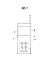
- the liquid crystal display device of the second embodiment can be formed substantially in a symmetrical shape bilaterally and the sizes of the left and right side portions can be reduced. For this reason, in a case of a portable telephone provided with this liquid crystal display device, as shown in FIG. 7, the display area 23 can be arranged at a central portion of the portable telephone main body 24 in a widthwise direction, thereby allowing improvement in design, allowing reduction of the size of the portable telephone main body 24 in a widthwise direction, and allowing improvement in portability.
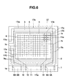
- Respective one end portions of flexible wiring board 41A and 41B are joined to the central portion of the lower side projecting portion 1a and the right side of the upper side projecting portion 1b of the active substrate 1.
- the input side connection terminals of he semiconductor integrated circuit devices 35, 36 and 37 are connected via wirings provided on the lower side projecting portion 1a to the flexible wiring board 41A, and the input side connection terminals of the semiconductor integrated circuit device 38 are connected via wirings (not shown) provided on the upper side projecting portion 1b to the flexible wiring board 41B.
Landscapes
- Physics & Mathematics (AREA)
- Nonlinear Science (AREA)
- Mathematical Physics (AREA)
- Chemical & Material Sciences (AREA)
- Crystallography & Structural Chemistry (AREA)
- General Physics & Mathematics (AREA)
- Optics & Photonics (AREA)
- Liquid Crystal (AREA)
- Devices For Indicating Variable Information By Combining Individual Elements (AREA)
Abstract
Description
Thin film transistors (not shown) and pixel electrodes (not shown) driven by the thin film transistors are disposed near crossing points of both the
Claims (16)
- A liquid crystal display device characterized by comprising:wherein the sealing member (3) has a first side portion extending generally in parallel to the first wires (6), the plurality of leading wires (7b, 7b1, 7b2, 27a, 27b, 28a, 28b, 30a, 30b) extend along the first side portion of the sealing member (3), and partial lines of the leading lines are formed on an area overlapping on the first side portion of the sealing member (3).a first substrate (2);a second substrate (1) having a face opposing to the first substrate;a frame-shaped sealing member (3) which bonds the first and second substrates (1, 2) to each other;liquid crystal (L) which is sealed in a space defined by the first and second substrates (1, 2) and the sealing member (3); anda plurality of first wires (6), a plurality of second wires (5) formed in a direction perpendicular to the first wires (6), and a plurality of leading wires (7b, 7b1, 7b2, 27a, 27b, 28a, 28b, 30a, 30b) which extend generally in parallel to the first wires (6) and which are respectively connected to corresponding one of the second wires (5),
- A liquid crystal display device according to claim 1, characterized in that the second substrate (1) has one side portion (1a) which is not opposed to the first substrate (2) and an integrated circuit (8, 8A, 8B, 31) connected to the plurality of first wires (6) and the plurality of leading wires (7b, 7b1, 7b2, 27a, 27b, 28a, 28b, 30a, 30b) is on the one side portion (1a).
- A liquid crystal display device according to claim 1, characterized in that a frame-shaped light shielding film (17) defining a display area (4) is formed on the first substrate (2), and the light shielding film (17) is formed so as not to overlap on the first side portion of the sealing member (3).
- A liquid crystal display device according to claim 3, characterized in that the light shielding film (17) is formed at a position spaced from the first side portion of the sealing member (3) by a distance of 0.2 mm or less.
- A liquid crystal display device according to claim 1, characterized by further comprising a sealing member diffusion preventing wall (21) provided outside the sealing member (3).
- A liquid crystal display device according to claim 5, characterized by further comprising a spacer (20) disposed between the first substrate (2) and the second substrate (1), wherein the spacer (20) is formed of the same material as the sealing member diffusion preventing wall (21).
- A liquid crystal display device according to claim 1, characterized in that the sealing member (3) has a second side portion which is opposed to the first side portion and which is generally parallel to the first side portion, partial lines of the plurality of leading wires (7b2, 27b, 30a, 30b) extend along the second side portion of the sealing member (3), and at least partial wires thereof are formed on an area overlapping the second side portion of the sealing member (3).
- A liquid crystal display device according to claim 7, characterized in that the second substrate (1) has one side portion (1a) which is not opposed to the first substrate (2), and a semiconductor integrated circuit (8b, 31, 34, 37, 38) connected to the plurality of first lines (6) and the plurality of leading lines (7b2, 27b, 30a, 30b) are mounted on the one side portion (1a).
- A liquid crystal display device, characterized by comprising:an active substrate (1) provided with a plurality of scanning signal lines (5), a plurality of data signal lines (6) formed in a direction perpendicular to the scanning signal lines (5), and a plurality of leading lines (7b, 7b1, 7b2, 27a, 27b, 28a, 28b, 30a, 30b) connected to corresponding one of the scanning signal lines (5);an opposing substrate (2) having a face opposed to the active substrate (1);a frame-shaped sealing member (3) which bonds the active substrate (1) and the opposing substrate (2);liquid crystal (L) disposed inside a space defined by the active substrate (1), the opposing substrate (2) and the sealing member (3); anda frame-shaped light shielding film (17) which is formed on the opposing substrate (2) and defines a display area (4),wherein the sealing member (3) has a first side portion which is generally perpendicular to the scanning signal lines (5),the leading lines (7b, 7b1, 7b2, 27a, 27b, 28a, 28b, 30a, 30b) are formed along the first side portion of the sealing member (3), andat least an area of the light shielding film (17) which corresponds to the first side portion of the sealing member (3) is formed inside the first side portion of the sealing member (3) so as to have a gap from the first side portion of the sealing member (3).
- A liquid crystal display device according to claim 9, characterized in that the active substrate (1) has one side portion (1a, 1b) which is not opposed to the opposing substrate (2), and a semiconductor integrated circuit (8, 8A, 8B, 31, 34, 36, 37, 38) connected to the plurality of data signal lines (6) and the plurality of leading lines (7b, 7b1, 7b2, 27a, 27b, 28a, 28b, 30a, 30b) is mounted on the one side portion.
- A liquid crystal display device according to claim 9, characterized in that an area of the light shielding film (17) which corresponds to the first side portion of the sealing member (3) is formed at a position spaced from the first side portion of the sealing member (3) by a distance of 0.2 mm or less.
- A liquid crystal display device according to claim 9, characterized in that partial lines of the leading lines (7b, 7b1, 7b2, 27a, 27b, 28a, 28b, 30a, 30b) are formed on an area overlapping on the first side portion of the sealing member (3).
- A liquid crystal display device according to claim 9, characterized in that the sealing member (3) has a second side portion which is provided on a side opposed to the first side portion and which is generally parallel to the first side portion, and partial lines of the plurality of leading lines (7b2, 27b, 30a, 30b) extend along the second side portion and other partial lines thereof are formed on an area overlapping on the second side portion of the sealing member.
- A liquid crystal display device, characterized by comprising:an opposing substrate (2);an active substrate (1) which is provided with a plurality of scanning signal lines (5), a plurality of data signal lines (6) formed in a direction perpendicular to the scanning signal lines (5), and a plurality of leading lines (7b, 7b1, 7b2, 27a, 27b, 28a, 28b, 30a, 30b) connected to corresponding one of the scanning signal lines (5), and which has a face opposed to the opposing substrate (2) and an one-side portion (1a, 1b) which is not opposed to the opposing substrate (2);a frame-shaped sealing member (3) which bonds the active substrate (1) and the opposing substrate (2);liquid crystal (L) disposed inside a space defined by the active substrate (1), the opposing substrate (2) and the sealing member (3); anda frame-shaped light shielding film (17) which is formed on the opposing substrate (2) and defines a display area (4),wherein the sealing member (3) has a pair of side portions which are generally perpendicular to the scanning signal lines (5), respectively,the leading lines (7b, 7b1, 7b2, 27a, 27b, 28a, 28b, 30a, 30b) are formed along respective side portions of the sealing member (3), and at least partial lines thereof are formed on an area overlapping on one of the side portions of the sealing member (3), anda semiconductor integrated circuit (8A, 8B, 11, 31, 33, 34, 35, 36, 37, 38) connected to the data signal lines (6) and the leading lines (7b1, 7b2, 27a, 27b, 28a, 28b, 30a, 30b) is mounted on the one-side portion of the active substrate (1).
- A liquid crystal display device, characterized by comprising:an opposing substrate (2);an active substrate (1) which is provided with a plurality of scanning signal lines (5), a plurality of data signal lines (6) formed in a direction perpendicular to the scanning signal lines (5), and a plurality of leading lines (27a, 27b, 28a, 28b, 30a, 30b) connected to corresponding scanning signal lines (5), and which has a face which is opposed to the opposing substrate (2), a first side portion (1a) which is not opposed to the opposing substrate (2), and a second side portion (1b) which is opposed to the first side portion (1a);a frame-shaped sealing member (3) which bonds the active substrate (1) and the opposing substrate (2);liquid crystal (L) disposed inside a space defined by the active substrate (1), the opposing substrate (2) and the sealing member (3);a frame-shaped light shielding film (17) which is formed on the opposing substrate (2) and defines a display area (4);a first semiconductor integrated circuit (33, 35) which is mounted on the first side portion (1a) of the active substrate (1) and which is connected to the data signal lines (6); anda second semiconductor integrated circuit (34, 38) which is mounted on the second side portion (1b) of the active substrate (1) and which is connected to the leading lines (27a, 27b, 28b, 30b),wherein the sealing member (3) has a pair of side portions which are generally perpendicular to the scanning signal lines (5), andthe leading lines (27a, 27b, 28a, 28b, 30a, 30b) are formed along respective side portions of the sealing member (3), and at least partial lines thereof are formed on an area overlapping on one side portion of the sealing member (3).
- A liquid crystal display device, characterized by comprising:an opposing substrate (2);an active substrate (1) which is provided with a plurality of scanning signal lines (5), a plurality of data signal lines (6) formed in a direction perpendicular to the scanning signal lines (5), and a plurality of leading lines (28a, 28b, 30a, 30b) connected to corresponding scanning signal lines (5), and which has a face which is opposed to the opposing substrate (2), a first side portion (1a) which is not opposed to the opposing substrate (2), and a second side portion (1b) which is opposed to the first side portion (1a);a frame-shaped sealing member (3) which bonds the active substrate (1) and the opposing substrate (2);liquid crystal (L) disposed inside a space defined by the active substrate (1), the opposing substrate (2) and the sealing member (3);a frame-shaped light shielding film (17) which is formed on the opposing substrate (2) and defines a display area (4);a first semiconductor integrated circuit (35) which is mounted on the first side portion (1a) of the active substrate (1) and which is connected to the data signal lines (6);a second semiconductor integrated circuit (36, 37) which is mounted on the first side portion (1a) of the active substrate (1) and which is connected to partial lines (28a, 30a) of the leading lines (28a, 28b, 30a, 30b); anda third semiconductor integrated circuit (38) which is mounted on the second side portion (1b) of the active substrate (1) and which is connected to the other partial lines (28b, 30b) of the leading lines (28a, 28b, 30a, 30b),wherein the sealing member (3) has a pair of side portions which are generally perpendicular to the scanning signal lines (5), respectively,the leading lines (36, 37) connected to the second semiconductor integrated circuit are formed along respective side portions of the sealing member (3), at least partial lines thereof are formed on an area overlapping on one side portion of the sealing member (3), the leading lines (28b, 30b) connected to the third semiconductor integrated circuit (38) are formed along respective side portions of the sealing member (3) and at least partial lines thereof are formed on an area overlapping on one side portion of the sealing member (3).
Applications Claiming Priority (6)
| Application Number | Priority Date | Filing Date | Title |
|---|---|---|---|
| JP2000224797 | 2000-07-26 | ||
| JP2000224797A JP2002040461A (en) | 2000-07-26 | 2000-07-26 | Liquid crystal display |
| JP2000289986A JP3896780B2 (en) | 2000-09-25 | 2000-09-25 | Manufacturing method of liquid crystal display device |
| JP2000289986 | 2000-09-25 | ||
| JP2001037808A JP3786180B2 (en) | 2001-02-15 | 2001-02-15 | Liquid crystal display |
| JP2001037808 | 2001-02-15 |
Publications (2)
| Publication Number | Publication Date |
|---|---|
| EP1176456A2 true EP1176456A2 (en) | 2002-01-30 |
| EP1176456A3 EP1176456A3 (en) | 2003-06-04 |
Family
ID=27344170
Family Applications (1)
| Application Number | Title | Priority Date | Filing Date |
|---|---|---|---|
| EP01118036A Withdrawn EP1176456A3 (en) | 2000-07-26 | 2001-07-25 | Liquid crystal display device having non-display area with reduced width |
Country Status (6)
| Country | Link |
|---|---|
| US (1) | US6747724B2 (en) |
| EP (1) | EP1176456A3 (en) |
| KR (1) | KR100500186B1 (en) |
| CN (1) | CN1170194C (en) |
| HK (1) | HK1043204A1 (en) |
| TW (1) | TWI300506B (en) |
Cited By (3)
| Publication number | Priority date | Publication date | Assignee | Title |
|---|---|---|---|---|
| EP1814159A3 (en) * | 2006-01-27 | 2007-10-24 | Samsung SDI Co., Ltd. | Flat panel display device and method of making the same |
| US7948177B2 (en) | 2006-01-27 | 2011-05-24 | Samsung Mobile Display Co., Ltd. | Flat panel display device with protective layer structure and method of making the same |
| US8035300B2 (en) | 2006-01-27 | 2011-10-11 | Samsung Mobile Display Co., Ltd. | Flat panel display device and method of making the same |
Families Citing this family (27)
| Publication number | Priority date | Publication date | Assignee | Title |
|---|---|---|---|---|
| JP3642304B2 (en) * | 2001-08-09 | 2005-04-27 | セイコーエプソン株式会社 | Liquid crystal panel, liquid crystal device and electronic device |
| US7295280B2 (en) * | 2001-09-03 | 2007-11-13 | Hannstar Display Corp. | Method of manufacturing one drop fill liquid crystal display panel |
| JP3959253B2 (en) * | 2001-10-02 | 2007-08-15 | 株式会社日立製作所 | Liquid crystal display device and portable display device |
| US6791660B1 (en) * | 2002-02-12 | 2004-09-14 | Seiko Epson Corporation | Method for manufacturing electrooptical device and apparatus for manufacturing the same, electrooptical device and electronic appliances |
| KR100885840B1 (en) * | 2002-03-23 | 2009-02-27 | 엘지디스플레이 주식회사 | Liquid crystal panel structure capable of compensating cell gap |
| JP4006284B2 (en) * | 2002-07-17 | 2007-11-14 | 株式会社 日立ディスプレイズ | Liquid crystal display |
| US7050131B2 (en) * | 2002-10-17 | 2006-05-23 | Lg.Philips Lcd Co., Ltd. | Liquid crystal display device having black seal pattern and external resin pattern, and method of fabricating the same |
| US6956550B2 (en) * | 2003-02-05 | 2005-10-18 | Giantplus Technology Co., Ltd. | Drive module of liquid crystal panel |
| US20040174488A1 (en) * | 2003-03-07 | 2004-09-09 | Shang-Kung Tsai | Symmetrical liquid crystal display panel |
| US8665247B2 (en) * | 2003-05-30 | 2014-03-04 | Global Oled Technology Llc | Flexible display |
| TWI306520B (en) * | 2003-06-09 | 2009-02-21 | Chunghwa Picture Tubes Ltd | Seal curing method of liquid crystal display and peripheral circuits thereof |
| KR20050005881A (en) * | 2003-07-07 | 2005-01-15 | 삼성전자주식회사 | Liquid crystal display device |
| CN1297840C (en) * | 2004-03-25 | 2007-01-31 | 友达光电股份有限公司 | Wire structure of the display |
| KR100752950B1 (en) * | 2004-04-30 | 2007-08-30 | 엘지.필립스 엘시디 주식회사 | CIO structure liquid crystal display device and manufacturing method |
| KR100732105B1 (en) | 2004-05-28 | 2007-06-27 | 도시바 마쯔시따 디스플레이 테크놀로지 컴퍼니, 리미티드 | Liquid crystal display panel and method for driving the same |
| CN100468484C (en) * | 2005-06-13 | 2009-03-11 | 友达光电股份有限公司 | mobile information device and display with narrow frame |
| CN101188081B (en) * | 2005-06-13 | 2010-09-15 | 友达光电股份有限公司 | Mobile information device and its display with narrow frame |
| JP5352403B2 (en) * | 2009-09-29 | 2013-11-27 | 株式会社ジャパンディスプレイ | Liquid crystal display device and manufacturing method thereof |
| JP5621283B2 (en) * | 2010-03-12 | 2014-11-12 | セイコーエプソン株式会社 | Electro-optical device and electronic apparatus |
| KR101107174B1 (en) * | 2010-03-23 | 2012-01-25 | 삼성모바일디스플레이주식회사 | Display panel and manufacturing method thereof |
| JP5971679B2 (en) | 2011-11-21 | 2016-08-17 | 株式会社ジャパンディスプレイ | Liquid crystal display |
| JP6116882B2 (en) * | 2012-12-10 | 2017-04-19 | 株式会社ジャパンディスプレイ | Liquid crystal display device and manufacturing method thereof |
| KR102512721B1 (en) | 2016-04-05 | 2023-03-23 | 삼성디스플레이 주식회사 | Display apparatus |
| CN107037644A (en) * | 2017-06-05 | 2017-08-11 | 京东方科技集团股份有限公司 | Display base plate motherboard and preparation method thereof, display base plate, panel and device |
| JP2020160321A (en) * | 2019-03-27 | 2020-10-01 | 株式会社ジャパンディスプレイ | Display device |
| WO2021106320A1 (en) | 2019-11-29 | 2021-06-03 | 株式会社ジャパンディスプレイ | Display device |
| JP2025030160A (en) * | 2023-08-23 | 2025-03-07 | 株式会社ジャパンディスプレイ | Liquid crystal panel, liquid crystal panel device, and imaging device |
Family Cites Families (18)
| Publication number | Priority date | Publication date | Assignee | Title |
|---|---|---|---|---|
| US3473147A (en) * | 1965-05-21 | 1969-10-14 | Bliss Co | Traffic actuated control system having a control unit for each traffic phase |
| JP2600929B2 (en) | 1989-01-27 | 1997-04-16 | 松下電器産業株式会社 | Liquid crystal image display device and method of manufacturing the same |
| JPH06214241A (en) * | 1993-01-18 | 1994-08-05 | Canon Inc | Liquid crystal display device |
| JPH0682811A (en) * | 1992-07-15 | 1994-03-25 | Toshiba Corp | Liquid crystal display device |
| JP2753549B2 (en) | 1994-06-21 | 1998-05-20 | カシオ計算機株式会社 | Liquid crystal display device |
| JP3552780B2 (en) * | 1995-02-28 | 2004-08-11 | ソニー株式会社 | Liquid crystal display |
| JPH08297286A (en) * | 1995-04-26 | 1996-11-12 | Internatl Business Mach Corp <Ibm> | Liquid crystal display |
| US5680192A (en) * | 1995-06-23 | 1997-10-21 | Garmin Corporation | Electro-optical display device with enlarged viewing area and single-sided driver connection |
| KR970007446A (en) * | 1995-07-10 | 1997-02-21 | 다까노 야스아끼 | Display device and manufacturing method of liquid crystal display device |
| TW505801B (en) * | 1995-10-12 | 2002-10-11 | Hitachi Ltd | In-plane field type liquid crystal display device comprising a structure prevented from charging with electricity |
| JPH10161136A (en) * | 1996-12-05 | 1998-06-19 | Sony Corp | Liquid crystal display device and manufacturing method thereof |
| US5831710A (en) * | 1997-02-06 | 1998-11-03 | International Business Machines Corporation | Liquid crystal display |
| TW375689B (en) * | 1997-03-27 | 1999-12-01 | Toshiba Corp | Liquid crystal display device and method for manufacturing the same |
| KR100277309B1 (en) * | 1997-06-13 | 2001-01-15 | 마찌다 가쯔히꼬 | Liquid Crystal Display and Manufacturing Method Thereof |
| TW475078B (en) * | 1997-09-30 | 2002-02-01 | Toshiba Corp | Liquid crystal display device and production of liquid crystal display device |
| JPH11223829A (en) * | 1998-02-09 | 1999-08-17 | Seiko Epson Corp | Liquid crystal device |
| TW561292B (en) | 1998-04-01 | 2003-11-11 | Seiko Epson Corp | Liquid crystal device, method for manufacturing the liquid crystal device, and electronic apparatus |
| US6407783B1 (en) * | 1998-04-07 | 2002-06-18 | Optrex Corporation | Liquid crystal display device |
-
2001
- 2001-07-23 US US09/910,752 patent/US6747724B2/en not_active Expired - Lifetime
- 2001-07-25 KR KR10-2001-0044716A patent/KR100500186B1/en not_active Expired - Fee Related
- 2001-07-25 EP EP01118036A patent/EP1176456A3/en not_active Withdrawn
- 2001-07-26 CN CNB011203331A patent/CN1170194C/en not_active Expired - Fee Related
- 2001-07-26 TW TW090118285A patent/TWI300506B/en not_active IP Right Cessation
-
2002
- 2002-07-09 HK HK02105094.2A patent/HK1043204A1/en unknown
Cited By (4)
| Publication number | Priority date | Publication date | Assignee | Title |
|---|---|---|---|---|
| EP1814159A3 (en) * | 2006-01-27 | 2007-10-24 | Samsung SDI Co., Ltd. | Flat panel display device and method of making the same |
| US7586259B2 (en) | 2006-01-27 | 2009-09-08 | Samsung Sdi Co., Ltd. | Flat panel display device and method of making the same |
| US7948177B2 (en) | 2006-01-27 | 2011-05-24 | Samsung Mobile Display Co., Ltd. | Flat panel display device with protective layer structure and method of making the same |
| US8035300B2 (en) | 2006-01-27 | 2011-10-11 | Samsung Mobile Display Co., Ltd. | Flat panel display device and method of making the same |
Also Published As
| Publication number | Publication date |
|---|---|
| HK1043204A1 (en) | 2002-09-06 |
| EP1176456A3 (en) | 2003-06-04 |
| US20020030784A1 (en) | 2002-03-14 |
| CN1334479A (en) | 2002-02-06 |
| CN1170194C (en) | 2004-10-06 |
| KR20020010503A (en) | 2002-02-04 |
| TWI300506B (en) | 2008-09-01 |
| KR100500186B1 (en) | 2005-07-14 |
| US6747724B2 (en) | 2004-06-08 |
Similar Documents
| Publication | Publication Date | Title |
|---|---|---|
| US6747724B2 (en) | Liquid crystal display device having non-display area with reduced width | |
| JP3276557B2 (en) | Liquid crystal display | |
| US6922226B2 (en) | Liquid crystal display device implementing improved electrical lines and the fabricating method | |
| CN104704546B (en) | Semiconductor device and display device | |
| US9097920B2 (en) | Display device | |
| CN102062975A (en) | Liquid crystal display device | |
| US6930741B2 (en) | LCD device having scanning lines and common lines | |
| JP5018407B2 (en) | LCD panel | |
| JP4074695B2 (en) | Liquid crystal display | |
| JPH09113922A (en) | Liquid crystal display device and method of manufacturing the same | |
| CN103080994B (en) | Display panel, and method for producing same | |
| JP4370806B2 (en) | Thin film transistor panel and manufacturing method thereof | |
| US20120170242A1 (en) | Circuit board, connecting structure of circuit boards, and display panel assembly | |
| JP2001021918A (en) | Liquid crystal display | |
| US7009676B1 (en) | Structure of a pad in a liquid crystal display device and a method for manufacturing thereof | |
| JP4275937B2 (en) | Liquid crystal device and manufacturing method thereof | |
| JP3861120B2 (en) | Liquid crystal display | |
| JP3365305B2 (en) | Semiconductor chip, its mounting structure and liquid crystal display device | |
| JP3786180B2 (en) | Liquid crystal display | |
| JP3538844B2 (en) | Liquid crystal device, method of manufacturing liquid crystal device, and electronic equipment | |
| JPH0815716A (en) | Liquid crystal display | |
| JP4765424B2 (en) | Liquid crystal display panel and liquid crystal display device using the same | |
| JP4201052B2 (en) | Liquid crystal display device and electronic apparatus using the same | |
| JP5026883B2 (en) | Electro-optical device and electronic apparatus | |
| JP2006091504A (en) | Electro-optical device and electronic apparatus |
Legal Events
| Date | Code | Title | Description |
|---|---|---|---|
| PUAI | Public reference made under article 153(3) epc to a published international application that has entered the european phase |
Free format text: ORIGINAL CODE: 0009012 |
|
| 17P | Request for examination filed |
Effective date: 20010725 |
|
| AK | Designated contracting states |
Kind code of ref document: A2 Designated state(s): AT BE CH CY DE DK ES FI FR GB GR IE IT LI LU MC NL PT SE TR |
|
| AX | Request for extension of the european patent |
Free format text: AL;LT;LV;MK;RO;SI |
|
| PUAL | Search report despatched |
Free format text: ORIGINAL CODE: 0009013 |
|
| AK | Designated contracting states |
Designated state(s): AT BE CH CY DE DK ES FI FR GB GR IE IT LI LU MC NL PT SE TR |
|
| AX | Request for extension of the european patent |
Extension state: AL LT LV MK RO SI |
|
| 17Q | First examination report despatched |
Effective date: 20031106 |
|
| AKX | Designation fees paid |
Designated state(s): DE FR GB NL |
|
| STAA | Information on the status of an ep patent application or granted ep patent |
Free format text: STATUS: THE APPLICATION IS DEEMED TO BE WITHDRAWN |
|
| 18D | Application deemed to be withdrawn |
Effective date: 20041014 |