EP1176426A2 - Method of checking vehicle mounted electronic units - Google Patents
Method of checking vehicle mounted electronic units Download PDFInfo
- Publication number
- EP1176426A2 EP1176426A2 EP01401991A EP01401991A EP1176426A2 EP 1176426 A2 EP1176426 A2 EP 1176426A2 EP 01401991 A EP01401991 A EP 01401991A EP 01401991 A EP01401991 A EP 01401991A EP 1176426 A2 EP1176426 A2 EP 1176426A2
- Authority
- EP
- European Patent Office
- Prior art keywords
- data
- order
- signal
- frame
- port
- Prior art date
- Legal status (The legal status is an assumption and is not a legal conclusion. Google has not performed a legal analysis and makes no representation as to the accuracy of the status listed.)
- Granted
Links
- 238000000034 method Methods 0.000 title claims abstract description 17
- 238000012360 testing method Methods 0.000 claims abstract description 87
- 238000012545 processing Methods 0.000 claims description 15
- 238000010998 test method Methods 0.000 claims description 5
- 238000004891 communication Methods 0.000 abstract description 12
- 230000000737 periodic effect Effects 0.000 abstract description 7
- 230000005540 biological transmission Effects 0.000 description 2
- 238000004519 manufacturing process Methods 0.000 description 2
- 238000001514 detection method Methods 0.000 description 1
- 238000011161 development Methods 0.000 description 1
- 238000010586 diagram Methods 0.000 description 1
- 238000011282 treatment Methods 0.000 description 1
- 230000001960 triggered effect Effects 0.000 description 1
Images





Classifications
-
- G—PHYSICS
- G01—MEASURING; TESTING
- G01R—MEASURING ELECTRIC VARIABLES; MEASURING MAGNETIC VARIABLES
- G01R31/00—Arrangements for testing electric properties; Arrangements for locating electric faults; Arrangements for electrical testing characterised by what is being tested not provided for elsewhere
- G01R31/005—Testing of electric installations on transport means
- G01R31/006—Testing of electric installations on transport means on road vehicles, e.g. automobiles or trucks
Definitions
- the present invention relates to a method of checking electronic units mounted in a vehicle, e.g. a car.
- the invention also concerns a system comprising means for performing the above method.
- Microcomputer chips e.g. microprocessors or microcontrollers
- Such a microcomputer chip 2 can function as a controller unit operative on various controlled systems (not shown in the figures).
- Such a microcomputer chip 2 typically comprises programs for proper car functioning, and programs specifically developed for internal checking. When it is operational in the vehicle, the programs for vehicle control functions are launched, whereas when circuits are to be inspected, the checking programs for checking are started.
- the checking programs are designed such that they can be started only by inputting complex logic combinations at the microcomputer, the combination being chosen such that it does not occur during normal operation.
- an order signal may indicate e.g. that both the signal for detecting the inserted ignition key and the ignition switch are turned on. The signal order thus gives instruction to a test routine, and is delivered from a test machine 3 to an ignition input circuit 4 (IG input circuit) contained in an electronic unit 1 for cars.
- the test machine 3 may e.g.
- the microcomputer chip 2 functions according to a program specific to a test to be performed.
- the microcomputer chip 2 then returns a response signal to the test machine 3 via an output circuit e.g. a courtesy lamp driving circuit (courtesy LP driving circuit) 5.
- the test machine 3 can thus perform function tests, so as to determine whether the microcomputer chip 2 functions well and the input and output circuits work normally.
- Various input circuits, such as an ignition input circuit 4, and output circuits such as a courtesy lamp driving circuit 5, are commonly used in car electronic units. Consequently, these common circuits require no other specific equipment for testing.
- the above test method employs a serial communications system including the test machine 3 as a master system and the electronic unit 1 as a slave system. As shown in Fig.2, communications are periodically sent from the test machine 3 to the electronic unit 1 at a rate of 200 ms, irrespective of the presence or absence of an order (i.e. an instruction indicating whether a car-running program or a test program is launched).
- an order signal 7 is loaded on a periodically passing communication.
- an order signal indicating "no reference" is sent.
- the microcomputer chip 2 is designed so as to output a response signal 8 after a processing time of tm (within the limit of 10 ms).
- the tests for the functioning of the electronic unit 1 are thus performed by using a test machine 3, and carried out at the last step of the production process for the car electronic unit 1.
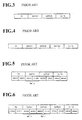
- Figs.3 and 4 show signal formats used in communications protocols in a known periodically performed transmission. Specifically, Fig.3 shows a format for order signal sent from the test machine 3 to the electronic unit 1, whereas Fig.4 shows a format for response signal sent from the electronic unit 1 to the test machine 3.
- reference ID indicates 8 bit data (B7 ⁇ B0) giving orders, the contents of which are explained in Table 1.
- ID Hexadecimal code Test mode B7 B6 B5 B4 B3 B2 B1 B0 No test 0 0 0 0 0 0 0 0 00
- Return the check sums calculated by ⁇ -computer 0 0 0 0 0 0 0 1 01 Read-out the state on SW input from common ports 0 0 0 0 0 1 0 02 Read-out the value from A/D ports 0 0 0 0 0 0 1 1 03 Write-in the output from common ports 0 0 0 0 0 1 0 0 04 Modify the periodicity of W/D pulses 0 0 0 0 0 0 1 0 1 05 End of the test mode 1 1 1 1 1 1 1 1 1 1 FF
- the common ports signify the ports common for input and output.
- the A/D ports signify analog/digital ports, through which voltages are measured, converted into digital terms and read out.
- the W/D pulses (watchdog pulses) are generated by integrated circuits provided beside the microcomputer, and watch out for disorders in the microcomputer.
- reference "DATA 1" stores data designating port numbers.
- DATA 1 when reading out the data regarding switch input for common ports (when ID is "0000 0010” in Table 1), DATA 1 comprise 8-bit data which designate a port, from which the state on switch input are read out.
- DATA 1 When reading out data from A/D ports (when ID is "0000 0011” in Table 1), DATA 1 comprise 8-bit data which designate a port, from which A/D values are read out.
- DATA 1 When writing-in output from common ports (when ID is "0000 0100” in Table 1), DATA 1 comprise 8-bit data which designate a port, from which the output is written in.
- DATA 2 and DATA 3 are supplied with different data, depending on test contents.
- an order signal shown in Fig.3 does not use DATA 2, so that all 8 bits of DATA 2 are supplied with a bit “0" (Fig.5).
- a response signal (Fig.4) to such an order signal DATA 2 is supplied, bit by bit, with a high-level /a low-level state of each of 8 terminals No.0 to 7 contained in the port, which is designated by "DATA 1" for reading out the state on switch input (see Fig.6).
- terminal No.0 corresponds to the lowest bit level
- terminal No.7 corresponds to the highest bit level.
- the port from which the input state regarding the switch is read out may be allocated port No.1 ("0000 0001"), and only terminal No.0 of this port may be put in a high state.
- "DATA 1" of the response signal is defined by bits “0000 0001”
- "DATA 2" is defined by bits "0000 0001”.
- the port, from which the input state regarding the switch is read out may be allocated port No.3 ("0000 0011"), and only terminal No.1 in this port may be put in a high state.
- "DATA 1" of the response signal is defined by bits “0000 0011”
- “DATA 2" thereof is defined by bits “0000 0010.
- "DATA 3" of the response signal of Fig.6 is not used, so that all the bits thereof are supplied with a bit "0".
- DATA 1 in the order signal of Fig.3 designates a port from which A/D values are read out.
- DATA 2 designates a terminal from which A/D values are read-out (Fig.7).
- terminal No.0 corresponds to the lowest bit level
- terminal No.7 corresponds to the highest bit level.
- the port from which A/D values are read out has port No.1 ("0000 0001), and only the A/D values of terminal No.0 in this port are read out.
- "DATA 2" in the order signal of Fig.3 is defined by an 8-bit content, which is intended to be written in to the microcomputer chip 2 (see Fig.9).
- "DATA 2" of Fig.10 is supplied with 8-bit data written in to the microcomputer chip 2 and outputted.
- "DATA 3" is not used, so that all the bits thereof are stored with a bit "0".
- Reference “C/S” in Figs.3 to 10 signifies check sum data.
- items “ID”, “DATA 1” and “DATA 2” are added, and the resulting lowest 8 bit data (i.e. value excluding the figures overflowing from 8 bits) are stored.
- the response signals Figs.13, 15, 17 and 19
- items “ID”, "DATA 1", “DATA 2” and “DATA 3” are added, and the resulting lowest 8 bit data are stored.
- a main object of the present invention is therefore to provide a method of testing a vehicle-borne electronic unit, in which one frame of order signal and one frame of response signal can process a greater number of ports and terminals, so that the overall processing time can be reduced.
- a method of testing an electronic unit mountable in a vehicle the method utilizing a test device and a controller unit included in the electronic unit, an order signal being supplied from the test device to the controller unit, and processed therein to give processed results; the latter being returned from the controller unit to the test device as a response signal.
- the above method comprises the steps of:
- the second data have a data length of 4 bits.
- the first data have a data length of 4 bits.
- the first step comprises providing an order signal containing third data designating a single port and having a data length of 4 bits, and several terminals, as well as fourth data instructing an order content relative to each of the terminals, and the step further comprises providing said third and fourth data in a frame of order signal.
- the fourth step may comprise providing a response signal containing the same data as the first and second data in the order signal.
- the invention further concerns a system for testing an electronic unit mountable in a vehicle, the system containing a test device and a controller unit included in the electronic unit, an order signal being supplied from the test device to the controller unit, and processed therein to give processed results; the latter being returned from the controller unit to the test device as a response signal.
- the above system comprises:
- the second data in the first means have a data length of 4 bits.
- the first data in the first means have a data length of 4 bits.
- the first means comprises means for providing an order signal containing third data designating a single port and having a data length of 4 bits, and several terminals, as well as fourth data instructing an order content relative to each of the terminals, and the means further comprises means for providing the third and fourth data in a frame of order signal.
- the fourth means comprises means for providing a response signal containing the same data as the first and second data in the order signal.
- a method of testing an electronic unit to be loaded in a vehicle such as a car according to a first embodiment of the invention
- four-bit data are processed between an electronic unit 1 and a test machine 3, instead of eight bit data handled in the past.
- one frame of order signal and of response signal can carry a greater number of ports and of terminals. Consequently, one processing cycle can handle several treatments, and the overall processing time can be reduced.
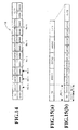
- Fig.11 a format for order signal according to the present embodiment (Fig.1(b)) and one known in the prior art (Fig.1(a)) are compared.
- the order format contains data with a fixed length of 48 bits. It includes item “ID” for indicating an order content, and items “DATA 1" to “DATA 9” for designating, inter alia, a port number. Each of these items contains data having a four-bit length. To them is added item “check sum (C/S)" having a eight bit length.
- ID Test mode B3 B2 B1 B0 Hexadecimal code No test 0 0 0 0 0 0
- C/S values calculated by ⁇ -computer 0 0 0 1 1 Read-out the data on SW input from common ports 0 0 1 0 2 Read-out the values from A/D ports 0 0 1 1 3 Write-in from the output of common ports 0 1 0 0 4 Modify the periodicity of W/D pulses 0 1 0 1 5 End of the test mode 1 1 1 1 1 F
- orders given in order signal "ID" contain seven types, including “no test” and "end of the test mode”.
- the occurrence probability P (a) of the order content "a” is 1/7.
- ID when "ID" is secured to have a data length of at least 3 bit, seven order contents can be distinguished.
- "ID" is actually secured with a 4-bit data length.
- port numbers As to be noted that a practically used microcomputer chip 2 contains around 5 ports only. The data having a 4 bit length can therefore designate distinctively those port numbers, according to the formula (I).
- "DATA 1" in the order signal 12 of Fig.13 contains 4-bit data designating the port number for reading out the A/D value.
- "DATA 2" and “DATA 3" are combined and processed as 8-bit data, and form a flag for designating a terminal in the port for reading out the A/D value, the port being designated by "DATA 1”.
- "DATA 4" and "DATA 5" are combined and processed as 8-bit data, and form a flag for designating another terminal in the port for reading out the A/D value, the port being designated by "DATA 1".
- terminal No.0 corresponds to the lowest bit level
- terminal No.7 corresponds to the highest bit level.
- "DATA 1" of the order signal 12 are provided with bits “0001”
- "DATA 2" and “DATA 3” thereof are respectively provided with bits “0000” and "0001”
- DATA 6" to "DATA 9” are not used, so that all the 4 bits included therein are provided with a bit"0", as shown in Fig.13.
- DATA 6" and DATA 7" are combined and processed as 8-bit data as shown in Fig.14, and are supplied with a port output content in 8 bits, which are intended to be written into the output writing-in port designated by "DATA 2".
- DATA 8" and “DATA 9” are combined and processed as 8-bit data as shown in Fig.14, and are supplied with a port output content in 8 bits, which are intended to be written into the output writing-in port designated by "DATA 3".
- Item “C/S” in Figs.11 to 14 indicate check sum data.
- 8 bit data combining, respectively, items “ID” and “DATA 1", items “DATA 2" and “DATA 3", items “DATA 4" and “DATA 5", items “DATA 6" and “DATA 7”, and items DATA 8 and DATA 9 are all added as 8-bit data. Then, the lowest 8-bit data (i.e. values excluding overflowed higher figures) are housed.
- the order signals 11 to 13 are produced in the test machine 3 shown in Fig.1, periodically transmitted to an electronic unit 1 for car loading at a 200 ms periodicity. They are inputted into a microcomputer chip 2 via an IG input circuit, both contained inside the electronic unit 1.
- Fig.15 shows a format for response signals known in the prior art, whilst Fig. (b) shows a format for response signals used in the present embodiment of the invention.
- the format for the response signals of the present embodiment is essentially the same as that for the order signals having a fixed data length of 48 bits. It contains item “ID” indicating a response content (same as the order content), and "DATA 1" to “DATA 9" each having a data length of 4 bits and designating, inter alia, port numbers. It further contains item “C/S” (check sum data) having a data length of 8 bits.
- ID includes a 4 bit data (B3 to B0) signifying the same order contents as shown in Table 2.
- Table 2 In the format for response signals of Fig. 15 (b), no test is carried out when "ID” is "0000" ("0" according to the hexadecimal code).
- the order content indicates a request for "return transmission of check-sum values”.
- the order content indicates "read out the input data on SW for common ports”.
- the order content indicates "read out the A/D port data”.
- terminals No.0 and No.7 correspond respectively to the lowest level bit and the highest level bit.
- terminal No.0 of port No.1 "0001"
- terminal No.1 of port No.2 "0010”
- terminal No.2 of port No.3 "0011"
- "DATA 1" in the response signals 15 contains 4 bit data designating the number for the port for reading out the A/D values, as shown in Fig.17.
- "DATA 2" and “DATA 3" are combined and processed as 8-bit data. The latter form a flag for designating one of the terminals contained in the port for reading out the A/D values, the port being designated by "DATA 1”.
- "DATA 4" and "DATA 5" are likewise combined and processed as 8-bit data, and form a flag for designating another terminal in the port for reading out the A/D values, the port being designated by "DATA 1".
- These "DATA 2 to DATA 5" in the response signals 15 correspond to "DATA 2" to "DATA 5" in the order signals 12 of Fig.13.
- "DATA 6" and "DATA 7" are also combined and processed as 8-bit data.
- "DATA 1" designates a port for reading out the A/D values.
- "DATA 2" and “DATA 3" in this port contain 8-bit data, designating 8-bit terminals for reading out the A/D values.
- "DATA 6" and DATA 7" are then supplied with 8-bit A/D values read-out from the above terminals.
- "DATA 8" and "DATA 9” are likewise combined and processed as 8-bit data.
- "DATA 1” designates a port for reading out the A/D values.
- "DATA 4" and “DATA 5" in this port contain 8-bit data designating 8-bit terminals for reading out the A/D values.
- "DATA 8” and DATA 9” are then supplied with 8-bit A/D values read-out from the above terminals.
- 8-bit data are designed to check whether the outputted data are the same as those in "DATA 4" and "DATA 5" in the order signal 13 of Fig.14.
- "DATA 6" and “DATA 7” are likewise combined and processed as 8-bit data, as shown in Fig.18.
- "DATA 2" designates a port for writing in the output.
- "DATA 6” and “DATA 7” are then supplied with a port output content in 8 bits, which has been written into the above designated port and read out therefrom.
- "DATA 8” and “DATA 9” are combined and processed as 8-bit data, as shown in Fig.18.
- "DATA 3" designates a port for writing in the output.
- "DATA 8” and “DATA 9” are then supplied with a port output content in 8 bits, which has been written into the above designated port and read out therefrom.
- Item “C/S” in Figs.15 to 18 signify check sum data.
- "ID” and “DATA 1", “DATA 2" and “DATA 3", “DATA 4" and “DATA 5", “DATA 6" and “DATA 7”, and “DATA 8” and “DATA 9” in the response signals 14 to 16 are respectively combined to form respective 8 bit data. All these 8 bit data are added, and the lowest 8 bit data (i.e. excluding higher figures which overflow from the sum) are obtained. "CS” is then supplied with these data.
- the response signals 14 to 16 are supplied from the electronic unit 1 to the test machine 3 through periodic communications.
- the response signals are checked in the test machine 3, to determine whether they contain relevant response contents which correspond to the order contents given in the order signals 11 to 13.
- the microcomputer chip 2 in the electronic unit 1 used in the present test system contains several ports 21, 22, each of which includes 8 terminals P00 to P17.
- the test machine shown in Fig.1 performs, prior to its shipment, testing of the electronic unit 1 to be loaded in a vehicle. During this testing, order signals are put on periodic communications running at a periodicity of 200 ms (see Fig.2).
- An order content is contained in item “ID” (Table 2) in an order signal and then transmitted.
- Each "ID” has a 4-bit length.
- the electronic unit 1 When reading out SW input data from a common port, the electronic unit 1 is supplied with "ID" data "0010" as an order signal 11 (Table 2, Fig.12). At the same time, "DATA 1" to “DATA 3" in the same order signal 11 are supplied with three corresponding 4-bit data, respectively designating a port for reading out the SW input state. "DATA 4" to “DATA 9” are supplied with a digit "0" in all of their bits. Further, signal “C/S” is supplied with check sum data.
- the order signal 11 thus comprises a fixed length of 48 bits, and is transmitted periodically. Accordingly, one frame of order signal 11 contains orders for reading out SW input data from 3 common ports for reading out the SW input state.
- the microcomputer chip 2 receives such an order signal 11 through an IG input circuit 4, and produces a response signal 14 (Fig.16) in reply thereto.
- DATA 4" and "DATA 5" are combined and processed as 8-bit data, as shown in Fig.16.
- DATA 1 designates a port for reading out the SW input state. This port contains 8 terminals having No.0 to 7. The high level/low level state of each of these 8 terminals are then supplied bit by bit in the combined DATA 4 and 5.
- "DATA 6" and "DATA 7" are combined and processed as 8-bit data. They are supplied bit by bit with the high level/low level state of each of 8 terminals No.0 to No.7 in the SW input state reading-out port designated by "DATA 2" (Fig.16).
- DATA 8" and "DATA 9" are combined and processed as 8-bit data.
- the response signal 14 thus includes a fixed length of 48 bits, and periodically transmitted to the test machine 3. One frame of the response signal 14 can thus contain the results of data reading-out from 3 common ports for reading out the state on SW input.
- one frame of respective order and response signal allows to perform a test for reading-out of SW input data for 3 common ports.
- the processing speed is thus tripled compared to the past, and the test and processing time for the car-borne electronic unit can be reduced greatly.
- one frame of order signal 12 contains an order for reading out the A/D port data for two terminals.
- the microcomputer chip 2 receives such an order signal 12 via the IG input circuit 4, and produces a response signal 15 in reply thereto.
- "DATA 6" and "DATA 7" are combined and processed as 8-bit data.
- "DATA 1" designates a port for reading out the A/D value
- "DATA 2" and “DATA 3” designate, by flag, a terminal for reading out the A/D values.
- the combined "DATA 6” and "DATA 7” are then supplied with 8-bit A/D read-out values for the above terminal.
- "DATA 8" and "DATA 9” are combined and processed as 8-bit data.
- "DATA 1” designates a port for reading out the A/D values
- "DATA 4" and "DATA 5" designate another terminal in the designated port.
- the combined "DATA 8" and "DATA 9” are then supplied with 8-bit A/D read-out values for the above terminal.
- C/S is supplied with check sum data.
- the fixed length of 48 bits thus obtained are periodically sent back to the test machine in a response signal 15. In this manner, one frame of response signal 15 allows A/D port data to be read out from two terminals in one A/D value read-out port.
- the A/D value are read out from two terminals and tested.
- the processing speed is thus doubled compared to the past processing practice, and the testing time for a car-loading electronic unit is greatly reduced.
- an order signal 13 of Fig.14 in the test machine 3 contains "ID” with digits "0100” (see Table 2). Meanwhile, "DATA 1" to “DATA 3" are supplied with three 4-bit data, respectively designating a port number for writing-in the output. As shown in Fig.14, “DATA 4" and “DATA 5" are combined and processed as 8-bit data. They are then supplied with a 8-bit length port output content which is intended to be written in to the port for writing-in the output, the port being designated by "DATA 1".
- DATA 6" and “DATA 7" are combined and processed as 8-bit data, and they are then supplied with a 8-bit length port output content which is intended to be written in to the port for writing-in the output, the port being designated by "DATA 2".
- DATA 8" and “DATA 9” are combined and processed as 8-bit data, and they are then supplied with a 8-bit length port output content which is intended to be written in to the port for writing-in the output, the port being designated by "DATA 3".
- C/S is supplied with check sum data. All these data are periodically communicated to the car-loading electronic unit 1.
- one frame of order signal 13 is designed to contain an order for writing-in the output from three common ports.
- the order signal 13 is entered in the car-loading electronic unit 1, and inputted into the microcomputer chip 2 via the IG input circuit 4.
- the microcomputer chip 2 produces a response signal 16 shown in Fig.18, in reply to the order signal.
- "ID" and "DATA 1" to “DATA 3" in the response signal 16 are supplied with the same corresponding data as those in the order signal 13 shown in Fig.14.
- "DATA 4" and "DATA 5" are combined and processed as 8-bit data, as shown in Fig.18. They are then supplied with a 8-bit length port output content, which was first written in to the output writing-in port designated by "DATA 1", and then read out therefrom.
- "DATA 6" and "DATA 7" are also processed as above, and supplied with a 8-bit length port output content, which was first written in to the output writing-in port designated by "DATA 2", and then read out therefrom.
- "DATA 8” and "DATA 9” are likewise processed, and are supplied with a 8-bit length port output content, which was first written in to the output writing-in port designated by DATA 3, and then read out therefrom.
- C/S is housed with check sum data.
- a fixed length of 48 bits is periodically communicated to the test machine 3 as a response signal 16.
- the test machine 3 examines whether "DATA 4" to "DATA 9" in the order signal 13 of Fig.14 prepared by this machine, on one hand, and "DATA 4" to "DATA 9" in the response signal 16 of Fig.18 transmitted by the car-loading electronic unit 1 on the other, are the same.
- one frame of response signal 16 can contain information on the output writing-in result for three output writing-in ports.
- one frame of order signal 11, 12 or 13 and one frame of response signal 14, 15 or 16 respectively have a fixed length longer than that in the prior art (see Figs. 11 to 15).
- its length has no significant meaning.
- the above frame can increase the number of ports for reading out the input state of switch by three, the number of ports for writing-in the output from common ports by three, and the number of terminals for reading-out the value from A/D ports by two. The testing time is thus greatly reduced.
- Prior art Invention Reading-out the input state on SW from common ports 1 port 3 ports Writing-in the output from common ports 1 port 3 ports Reading-out the value from A/D ports 1 terminal 2 terminals
- the data length of at least part of data is shortened to 4 bits.
- one frame of order signal transmitted periodically from a car-borne electronic unit to a controller unit, can carry data designating an increased number of ports and terminals.
- the order signal is then processed by the controller unit.
- the processed results are loaded on a response signal and returned to the electronic unit and the test machine.
- several ports and several terminals can be processed and tested in a cycle of periodic communications.
- the present invention can greatly reduce the test time.
- the response signal contains the same data as the order signal, as to the data for the order contents, as well as the data for designating the ports and terminals. In this manner, data efficiency is improved, not only for the order signal, but also for the response signal.
Landscapes
- Chemical & Material Sciences (AREA)
- Engineering & Computer Science (AREA)
- Combustion & Propulsion (AREA)
- Physics & Mathematics (AREA)
- General Physics & Mathematics (AREA)
- Test And Diagnosis Of Digital Computers (AREA)
- Selective Calling Equipment (AREA)
- Small-Scale Networks (AREA)
- Time-Division Multiplex Systems (AREA)
- Maintenance And Management Of Digital Transmission (AREA)
Abstract
Description
| ID | Hexadecimal code | ||||||||
| Test mode | B7 | B6 | B5 | B4 | B3 | B2 | B1 | B0 | |
| No test | 0 | 0 | 0 | 0 | 0 | 0 | 0 | 0 | 00 |
| Return the check sums calculated by µ-computer | 0 | 0 | 0 | 0 | 0 | 0 | 0 | 1 | 01 |
| Read-out the state on SW input from common ports | 0 | 0 | 0 | 0 | 0 | 0 | 1 | 0 | 02 |
| Read-out the value from A/D ports | 0 | 0 | 0 | 0 | 0 | 0 | 1 | 1 | 03 |
| Write-in the output from common ports | 0 | 0 | 0 | 0 | 0 | 1 | 0 | 0 | 04 |
| Modify the periodicity of W/D pulses | 0 | 0 | 0 | 0 | 0 | 1 | 0 | 1 | 05 |
| End of the | 1 | 1 | 1 | 1 | 1 | 1 | 1 | 1 | FF |
| ID | |||||
| Test mode | B3 | B2 | B1 | B0 | Hexadecimal code |
| No test | 0 | 0 | 0 | 0 | 0 |
| Return the C/S values calculated by µ-computer | 0 | 0 | 0 | 1 | 1 |
| Read-out the data on SW input from common ports | 0 | 0 | 1 | 0 | 2 |
| Read-out the values from A/D ports | 0 | 0 | 1 | 1 | 3 |
| Write-in from the output of common ports | 0 | 1 | 0 | 0 | 4 |
| Modify the periodicity of W/D pulses | 0 | 1 | 0 | 1 | 5 |
| End of the | 1 | 1 | 1 | 1 | F |
| Prior art | Invention | |
| Reading-out the input state on SW from | 1 | 3 ports |
| Writing-in the output from | 1 | 3 ports |
| Reading-out the value from A/ | 1 | 2 terminals |
Claims (10)
- A method of testing an electronic unit (1) mountable in a vehicle, the method utilizing a test device (3) and a controller unit (2) included in the electronic unit (1), an order signal being supplied from the test device (3) to the controller unit (2), and processed therein to give processed results; the latter being returned from the controller unit (2) to the test device (3) as a response signal, said method comprising the steps of:providing, in said test device (3), first data designating several ports and several terminals contained in said controller unit (2), as well as second data instructing an order content relative to each of said ports and terminals, and providing said first and second data in a frame of order signal, thereby formulating an order signal (11, 12, 13) containing order contents (first step);periodically transmitting said order signal (11, 12, 13) from said test device (3) to said controller unit (2), frame by frame, at a given frequency (second step);processing said order contents corresponding to each of said ports and terminals contained in said order signal (11, 12, 13), when said order signal is received by said controller unit (2), thereby obtaining processed results (third step);providing, in said controller unit (2), said processed results for each of said ports and terminals in a frame of response signal (fourth step); andperiodically returning said response signal (14, 15, 16) from said controller unit (2) to said test device (3), frame by frame, at said given frequency (fifth step).
- The method according to claim 1, wherein said second data have a data length of 4 bits.
- The method according to claim 1 or 2, wherein said first data have a data length of 4 bits.
- The method according to any one of claims 1 to 3, wherein said first step comprises providing an order signal (11, 12, 13) containing third data designating a single port and having a data length of 4 bits, and several terminals, as well as fourth data instructing an order content relative to each of said terminals, and said step further comprises providing said third and fourth data in a frame of order signal.
- The method according to any one of claims 1 to 4, wherein said fourth step comprises providing a response signal (14, 15, 16) containing the same data as said first and second data in said order signal.
- A system for testing an electronic unit (1) mountable in a vehicle, the system containing a test device (3) and a controller unit (2) included in the electronic unit (1), an order signal (11, 12, 13) being supplied from the test device (3) to the controller unit (2), and processed therein to give processed results; the latter being returned from the controller unit (2) to the test device (3) as a response signal, said system comprising:means for providing, in said test device (3), first data designating several ports and several terminals contained in said controller unit (2), as well as second data instructing an order content relative to each of said ports and terminals, and for providing said first and second data in a frame of order signal, such as to formulate an order signal (11, 12, 13) containing order contents (first means);means for periodically transmitting said order signal (11, 12, 13) from said test device (3) to said controller unit (2), frame by frame, at a given frequency (second means);means for processing said order contents corresponding to each of said ports and terminals contained in said order signal (11, 12, 13), when said order signal is received by said controller unit (2), such as to obtain processed results (third means);means for providing, in said controller unit (2), said processed results for each of said ports and terminals in a frame of response signal (fourth means); andmeans for periodically returning said response signal (14, 15, 16) from said controller unit (2) to said test device (3), frame by frame, at said given frequency (fifth means).
- The system according to claim 6, wherein said second data in said first means have a data length of 4 bits.
- The system according to claim 6 or 7, wherein said first data in said first means have a data length of 4 bits.
- The system according to any one of claims 6 to 8, wherein said first means comprises means for providing an order signal (11, 12, 13) containing third data designating a single port and having a data length of 4 bits, and several terminals, as well as fourth data instructing an order content relative to each of said terminals, and said means further comprises means for providing said third and fourth data in a frame of order signal.
- The system according to any one of claims 6 to 9, wherein said fourth means comprises means for providing a response signal (14, 15, 16) containing the same data as said first and second data in said order signal (11, 12, 13).
Applications Claiming Priority (2)
| Application Number | Priority Date | Filing Date | Title |
|---|---|---|---|
| JP2000225268A JP2002041322A (en) | 2000-07-26 | 2000-07-26 | Inspection method for in-vehicle electronic unit |
| JP2000225268 | 2000-07-26 |
Publications (3)
| Publication Number | Publication Date |
|---|---|
| EP1176426A2 true EP1176426A2 (en) | 2002-01-30 |
| EP1176426A3 EP1176426A3 (en) | 2004-01-14 |
| EP1176426B1 EP1176426B1 (en) | 2005-12-14 |
Family
ID=18719068
Family Applications (1)
| Application Number | Title | Priority Date | Filing Date |
|---|---|---|---|
| EP01401991A Expired - Lifetime EP1176426B1 (en) | 2000-07-26 | 2001-07-24 | Method of checking vehicle-mounted electronic units |
Country Status (4)
| Country | Link |
|---|---|
| US (1) | US6654702B2 (en) |
| EP (1) | EP1176426B1 (en) |
| JP (1) | JP2002041322A (en) |
| DE (1) | DE60115778T2 (en) |
Families Citing this family (1)
| Publication number | Priority date | Publication date | Assignee | Title |
|---|---|---|---|---|
| CN113395348B (en) * | 2021-06-11 | 2022-03-08 | 安谋科技(中国)有限公司 | Vehicle-mounted chip, functional fault checking method and electronic equipment |
Family Cites Families (16)
| Publication number | Priority date | Publication date | Assignee | Title |
|---|---|---|---|---|
| JPS5410813A (en) * | 1977-06-27 | 1979-01-26 | Toshiba Corp | Tester for electronic controller of automobile |
| US4521879A (en) * | 1977-11-25 | 1985-06-04 | Klaus Gueldenpfennig | Digital private branch exchange |
| JPS56149848A (en) * | 1980-04-23 | 1981-11-19 | Tokyo Sogo Keibi Hoshiyou Kk | Signal transmission system |
| US5896418A (en) * | 1983-06-16 | 1999-04-20 | Hitachi, Ltd. | Data transmission system having a communication control computer for controlling communication between a communication interface module and terminal devices |
| JP2513195B2 (en) | 1986-10-17 | 1996-07-03 | ソニー株式会社 | Inspection methods |
| KR910002804B1 (en) * | 1987-02-27 | 1991-05-04 | 미쓰비시지도오샤 고교 가부시끼가이샤 | Multi-function testor for self-diagnosis |
| JPH0776737B2 (en) * | 1988-10-21 | 1995-08-16 | 富士重工業株式会社 | Vehicle diagnostic system |
| JP2851879B2 (en) | 1989-09-19 | 1999-01-27 | 富士通株式会社 | Data communication device |
| EP0425199B1 (en) * | 1989-10-27 | 1996-06-19 | Hitachi, Ltd. | Motor vehicle control system and control unit thereof |
| JPH0442635A (en) * | 1990-06-08 | 1992-02-13 | Fujitsu Ltd | Packet communication system |
| JP3104459B2 (en) | 1993-03-15 | 2000-10-30 | 株式会社大林組 | Structure to prevent leakage of contaminated water at waste disposal sites |
| US5845145A (en) * | 1995-12-21 | 1998-12-01 | Apple Computer, Inc. | System for generating and sending a critical-world-first data response packet by creating response packet having data ordered in the order best matching the desired order |
| JPH10274602A (en) * | 1997-03-31 | 1998-10-13 | Toyota Motor Corp | Vehicle communication control device |
| JP2000156685A (en) * | 1998-11-18 | 2000-06-06 | Fuji Heavy Ind Ltd | Abnormality monitoring device for vehicle control system |
| US6256557B1 (en) * | 1998-11-25 | 2001-07-03 | Delphi Technologies, Inc. | Vehicle serial data bus communication protocol and method |
| US6279531B1 (en) * | 1999-08-09 | 2001-08-28 | Ford Global Technologies, Inc. | System and method for controlling engine torque |
-
2000
- 2000-07-26 JP JP2000225268A patent/JP2002041322A/en not_active Abandoned
-
2001
- 2001-07-24 EP EP01401991A patent/EP1176426B1/en not_active Expired - Lifetime
- 2001-07-24 DE DE60115778T patent/DE60115778T2/en not_active Expired - Fee Related
- 2001-07-25 US US09/911,546 patent/US6654702B2/en not_active Expired - Fee Related
Also Published As
| Publication number | Publication date |
|---|---|
| DE60115778D1 (en) | 2006-01-19 |
| JP2002041322A (en) | 2002-02-08 |
| US20020035420A1 (en) | 2002-03-21 |
| US6654702B2 (en) | 2003-11-25 |
| EP1176426B1 (en) | 2005-12-14 |
| DE60115778T2 (en) | 2006-09-07 |
| EP1176426A3 (en) | 2004-01-14 |
Similar Documents
| Publication | Publication Date | Title |
|---|---|---|
| US5012180A (en) | System for testing internal nodes | |
| JP4149806B2 (en) | Equipment for monitoring the processor | |
| US6961671B2 (en) | System and a method for preventing tampering with a recorded accumulated running distance of a vehicle | |
| US4554461A (en) | Information transmitting apparatus | |
| US5153509A (en) | System for testing internal nodes in receive and transmit FIFO's | |
| US6519516B2 (en) | Method and device for safeguarding against manipulation of an odometer or a trip recorder | |
| US5696776A (en) | Data transmission method in a real-time data processing system | |
| EP1176426B1 (en) | Method of checking vehicle-mounted electronic units | |
| US4604620A (en) | Information transmission system | |
| US5510775A (en) | Method of personalizing an electronic module and electronic circuit and module for implementing the method | |
| US7375623B2 (en) | Method for monitoring at least one sensor | |
| US20090100306A1 (en) | Electronic unit | |
| JPH07210237A (en) | In-vehicle electronic control circuit self-diagnosis device | |
| JPH0257676B2 (en) | ||
| JPS63243832A (en) | Multifunctional tester for self-diagnosis | |
| US6986082B2 (en) | Testing system for semiconductor memory device | |
| JP2806026B2 (en) | Memory test circuit | |
| JPS61273677A (en) | Collecting system for system information | |
| JPH03114942A (en) | Abnormality detecting device for on board control unit | |
| JPS61273678A (en) | Collecting system for system information | |
| JPS6321930B2 (en) | ||
| KR890003766B1 (en) | Dial pulse transmitting method and circuit | |
| JPH0722281B2 (en) | Data communication method between in-vehicle computers | |
| KR0174008B1 (en) | Data communication device for self diagnosis operation | |
| JP2009248938A (en) | On-vehicle electronic control apparatus |
Legal Events
| Date | Code | Title | Description |
|---|---|---|---|
| PUAI | Public reference made under article 153(3) epc to a published international application that has entered the european phase |
Free format text: ORIGINAL CODE: 0009012 |
|
| 17P | Request for examination filed |
Effective date: 20010728 |
|
| AK | Designated contracting states |
Kind code of ref document: A2 Designated state(s): AT BE CH CY DE DK ES FI FR GB GR IE IT LI LU MC NL PT SE TR |
|
| AX | Request for extension of the european patent |
Free format text: AL;LT;LV;MK;RO;SI |
|
| PUAL | Search report despatched |
Free format text: ORIGINAL CODE: 0009013 |
|
| AK | Designated contracting states |
Kind code of ref document: A3 Designated state(s): AT BE CH CY DE DK ES FI FR GB GR IE IT LI LU MC NL PT SE TR |
|
| AX | Request for extension of the european patent |
Extension state: AL LT LV MK RO SI |
|
| RIC1 | Information provided on ipc code assigned before grant |
Ipc: 7B 60R 16/02 B Ipc: 7G 06F 11/267 A Ipc: 7G 01R 31/00 B |
|
| 17Q | First examination report despatched |
Effective date: 20040708 |
|
| AKX | Designation fees paid |
Designated state(s): DE GB |
|
| GRAP | Despatch of communication of intention to grant a patent |
Free format text: ORIGINAL CODE: EPIDOSNIGR1 |
|
| RTI1 | Title (correction) |
Free format text: METHOD OF CHECKING VEHICLE-MOUNTED ELECTRONIC UNITS |
|
| GRAS | Grant fee paid |
Free format text: ORIGINAL CODE: EPIDOSNIGR3 |
|
| GRAA | (expected) grant |
Free format text: ORIGINAL CODE: 0009210 |
|
| AK | Designated contracting states |
Kind code of ref document: B1 Designated state(s): DE GB |
|
| REG | Reference to a national code |
Ref country code: GB Ref legal event code: FG4D |
|
| REF | Corresponds to: |
Ref document number: 60115778 Country of ref document: DE Date of ref document: 20060119 Kind code of ref document: P |
|
| PLBE | No opposition filed within time limit |
Free format text: ORIGINAL CODE: 0009261 |
|
| STAA | Information on the status of an ep patent application or granted ep patent |
Free format text: STATUS: NO OPPOSITION FILED WITHIN TIME LIMIT |
|
| 26N | No opposition filed |
Effective date: 20060915 |
|
| PGFP | Annual fee paid to national office [announced via postgrant information from national office to epo] |
Ref country code: DE Payment date: 20090716 Year of fee payment: 9 Ref country code: GB Payment date: 20090722 Year of fee payment: 9 |
|
| GBPC | Gb: european patent ceased through non-payment of renewal fee |
Effective date: 20100724 |
|
| PG25 | Lapsed in a contracting state [announced via postgrant information from national office to epo] |
Ref country code: DE Free format text: LAPSE BECAUSE OF NON-PAYMENT OF DUE FEES Effective date: 20110201 |
|
| REG | Reference to a national code |
Ref country code: DE Ref legal event code: R119 Ref document number: 60115778 Country of ref document: DE Effective date: 20110201 |
|
| PG25 | Lapsed in a contracting state [announced via postgrant information from national office to epo] |
Ref country code: GB Free format text: LAPSE BECAUSE OF NON-PAYMENT OF DUE FEES Effective date: 20100724 |