TECHNICAL FIELD
The present invention relates to a semiconductor
device and a method for manufacture thereof, and
more particularly to a semiconductor device including
an field effect transistor.
BACKGROUND ART
In an integrated circuit using SiMOS field
effect transistors (Si-MOSFET's), the coexistence of
the reduction in power consumption and the enhancement
in speed has been attained by making the reduction in
device dimension, the reduction in operating voltage
and so forth in accordance with a so-called scaling
rule.
However, there have arisen many problems
including the problem of a short-channel effect
generated in association with the reduction in dimension
and the problem of that deterioration of an
operation margin caused by the closeness of a drain
voltage and a threshold voltage to each other which
becomes remarkable in the case where the reduction in
voltage is contemplated.
Also, when eyes are turned to the mobility
which makes a barometer for the enhancement in speed,
the various improvements as mentioned above are
ironically enough caught in the result that the
mobility in Si in the real device is smaller than 100
or is far less than the value of mobility in bulk.
Thus, a further improvement of the performance
of the conventional Si-MOSFET has become very
difficult.
DISCLOSURE OF THE INVENTION
The further improvement in performance has a
need to contemplate the enhancement in speed by improving
a semiconductor material itself. One solution is
to use a so-called compound semiconductor which
provides a high speed in itself. However, this solution
is not realistic since it is very difficult to
combine the compound semiconductor technology with the
Si integrated circuit technology and the manufacture
cost becomes stupendous.
One object of the present invention is to
provide a semiconductor device having a field effect
transistor with a low power consumption and a high
speed by use of the combination of Si and an element
such as Ge, C or the like in the same group as that of
Si.
According to one aspect of the present invention,
a strain applying semiconductor layer applies a
strain to a channel forming layer in which a channel of
a field effect transistor is formed. Thereby, the
mobility of carriers in the channel is made larger than
the mobility of carriers in that material of the
channel forming layer which is unstrained. For
example, in the case where the material of the channel
forming layer is Si, the strain application makes the
in-plane lattice constant of the Si channel forming
layer larger than that of unstrained Si.
It has been suggested that the mobility of
carriers in Si or Ge applied with a strain may be
increased as compared with that in unstrained Si or Ge
(M. V. Fischetti and S. E. Laux: J. Appl. Phys. 80(4),
15 August 1996, pp. 2234-2252). This is known for long
or has the same origin as that of a phenomenon that the
deposition of Si on sapphire causes an increase in
mobility since Si is subjected to an in-plane strain.
In the one aspect of the present invention, this
phenomenon is put into practice to fabricate a field
effect transistor and a semiconductor device such as an
integrated circuit using the field effect transistor.
According to another aspect of the present
invention, there is provided a semiconductor device
having a p-type field effect transistor in which the
energy at a top of the valence band of the interface
between a channel forming layer and one of layers
adjacent to opposite surfaces of the channel forming
layer lying on a gate insulating film side of the
channel forming layer is made larger than that of the
interface between the channel forming layer and the
other adjoining layer lying on the other side of the
channel forming layer.
According to another aspect of the present
invention, there is provided a semiconductor device
having an n-type field effect transistor in which the
energy at a top of the conduction band of the interface
between a channel forming layer and one of layers
adjacent to opposite surfaces of the channel forming
layer lying on a gate insulating film side of the
channel forming layer is made smaller than that of the
interface between the channel forming layer and the
other adjoining layer lying on the other side of the
channel forming layer.
According to another aspect of the present
invention, there is provided a structure in which an
energy barrier for carriers in a channel of a field
effect transistor exists on a side of the channel
opposite to a gate insulating film, and the lattice of
a channel forming layer having the channel formed
therein is strained so that the mobility of carriers in
the channel is made larger than the mobility of
carriers in that material of the channel forming layer
which is unstrained.
BRIEF DESCRIPTION OF THE DRAWINGS
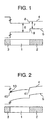
Fig. 1 is a diagram for explaining the
principle of operation of the present invention or a
band diagram of the multilayered structure of an SiO2
gate insulating film, a strained Si layer and an Si1-xGex
strain applying layer;
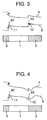
Fig. 2 is a band diagram in a state in which
a positive bias is applied to a gate of the structure
shown in Fig. 1;
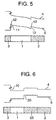
Fig. 3 is a band diagram in a state in which
a negative bias is applied to the gate of the structure
shown in Fig. 1;
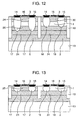
Fig. 4 is a band diagram in a state in which
a steep n-type doping is applied to the uppermost
portion of the Si1-xGex strain applying layer of the
structure shown in Fig. 1;
Fig. 5 is a band diagram in a state in which
a substrate biasing voltage is applied to the structure
shown in Fig. 1;
Fig. 6 is another diagram for explaining the
principle of operation of the present invention or a
band diagram of the multilayered structure of an SiO2
gate insulating film, a strained Si layer, a strained
Si1-yGey layer and an Si1-xGex strain applying layer;
Fig. 7 is a cross section showing the structure
of complementary field effect transistors according
to Embodiment 1 of the present invention;
Fig. 8 is a cross section showing the structure
of complementary field effect transistors according
to Embodiment 2 of the present invention;
Fig. 9 is a cross section showing the structure
of complementary field effect transistors according
to Embodiment 3 of the present invention;
Fig. 10 is a cross section showing the structure
of complementary field effect transistors according
to Embodiment 4 of the present invention;
Fig. 11 is a cross section showing the structure
of complementary field effect transistors according
to Embodiment 5 of the present invention;
Fig. 12 is a cross section showing the structure
of complementary field effect transistors according
to Embodiment 6 of the present invention;
Fig. 13 is a cross section showing the structure
of complementary field effect transistors according
to Embodiment 7 of the present invention;
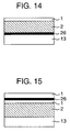
Fig. 14 is the cross section of an SOI
substrate according to Embodiment 8 of the present
invention;
Fig. 15 is the cross section of an SOI
substrate according to Embodiment 9 of the present
invention; and
Figs. 16a to 16d are cross sections showing
the manufacture steps of an SOI substrate according to
Embodiment 10 of the present invention.
BEST MODE FOR CARRYING OUT THE INVENTION
First, the description will be made of the
band structure of and the principle of operation of a
field effect transistor having a channel of Si
subjected to a strain. It is suitable to use Si1-xGex
(0 < x < 1) for a strain applying layer which applies
the strain to Si. Fig. 1 shows a band diagram of the
multilayered structure of an SiO2 gate insulating film
3, a strained Si layer 1 and an Si1-xGex strain applying
layer 2. The band diagram exhibits a band discontinuity
the type of which is such that the band gap 6 of
the strained Si layer 1 is wider than the band gap 7 of
the Si1-xGex strain applying layer 2 and the energies of
the valence band 5 and the conduction band 4 of the
strained Si layer 1 are both lowered.
Now, in the case of an n-type field effect
transistor, the application of a positive voltage to
the gate causes a band bend in the vicinity of the
interface between the gate insulating film 3 and the
strained Si layer 1, as shown in Fig. 2, so that
electrons are stored in a notch 10 of the conduction
band in the strained Si layer 1 formed in the bent
portion, thereby enabling a transistor operation. This
is quite the same as an ordinary MOS type field effect
transistor.
In the case of a p-type field effect
transistor, the application of a negative voltage to
the gate causes a band bend in the vicinity of the
interface between the gate insulating film 3 and the
strained Si layer 1, as shown in Fig. 3. However, more
holes are stored in a notch 12 of the valence band in
the Si1-xGex strain applying layer 2 formed in the
interface between the strained Si layer 1 and the
Si1-xGex strain applying layer 2 than a notch 11 of the
valence band in the strained Si layer 1 formed in the
bent portion. But, since the mobility of holes in the
Si1-xGex strain applying layer 2 is remarkably small as
compared with that in the strained Si layer 1, there is
a problem that the enhancement in speed cannot be
contemplated as compared with an ordinary MOS type
field effect transistor. Also, there is a problem that
in the case where complementary field effect transistors
are formed, it becomes difficult to balance p and
n channels with each other.
The above problems can be solved by reducing
the accumulation of holes in the notch 12 through the
following methods. In a first method, the source/drain
junction depth is made sufficiently shallower than the
thickness of the strained Si layer 1, thereby preventing
the effluence of holes into the Si1-xGex strain
applying layer 2. More particularly, for example, when
the thickness of the strained Si layer 1 is 70 nm, the
junction depth may be selected to be about 40 nm.
Since this is much the same as a value used in a short-channel
device having a channel length shorter than 0.1
microns, it is sufficiently realizable.
In a second method, a steep n-type doping,
preferably, with the doping depth in the range of 0.1
to 30 nm is applied in the vicinity of the interface
between the Si1-xGex strain applying layer 2 and the
strained Si layer 1. With this method, the energy
level at the top 43 of the notch 12 of the valence band
in the Si1-xGex strain applying layer 2 is lowered, as
shown in Fig. 4. For example, it becomes lower than
the energy level at the top 42 of the notch 11 of the
valence band in the strained Si layer 1. As a result,
the storage of holes in the notch 12 is reduced. This
method can also be realized by applying the n-type
doping to the strained Si layer 1 or both the strained
Si layer and the Si1-xGex strain applying layer 2. In
this case too, it is preferable that the doping depth
is in the range of 0.1 to 30 nm.
In a third method, a substrate biasing
voltage is controlled so that a positive voltage is
applied onto the Si1-xGex strain applying layer 2 side.
As shown in Fig. 5, this method provides a band structure
with a downward inclination on the right side,
that is, a falling on the Si1-xGex strain applying layer
2 side so that the energy level at the top 43 of the
notch 12 of the valence band in the Si1-xGex strain
applying layer 2 becomes lower than the energy level at
the top 42 of the notch 11 of the valence band in the
strained Si layer 1. As a result, the storage of holes
in the notch 12 is reduced.
As mentioned in the above, the prevention of
the effluence of holes from the strained Si channel
into the strain applying layer is a factor indispensable
to the realization of a p-type field effect
transistor or complementary field effect transistors.
Further, in order to contemplate the enhancement in
speed and the reduction in voltage, the employment of
the following construction is also effective. Namely,
the material of a drain region in the case of a p-type
field effect transistor or a source region in the case
of an n-type field effect transistor is selected to be
the same parent material as the Si1-xGex strain applying
layer or to have the same composition ratio as the
Si1-xGex strain applying layer. With such a construction,
a band discontinuity between the strained Si and
the SiGe causes a change in electric field distribution
between the source and the drain to enable the more
effective acceleration of carriers. Thereby, a further
enhancement in speed can be contemplated and the
reduction in pinch off voltage enables an operation at
a low voltage.
The description up to here has been made in
conjunction with a transistor using strained Si as a
channel for either electrons or holes. In connection
with holes, however, when strained Si1-yGey (0 < y ≦ 1)
is used as a channel, there is realized the further
increase in mobility, that is, the further enhancement
in speed. In the case where Si1-xGex is used for a
strain applying layer, Si formed as an overlying layer
on Si1-xGex is applied with an in-plane tensile strain
while Si1-yGey formed as an overlying layer on Si1-xGex is
applied with an in-plane compressive strain.
In the case where a strained Si1-yGey layer 25,
a strain Si layer 1 and a gate insulating film 3 are
formed in the mentioned order on an Si1-xGex strain
applying layer 2 so that they overlie each other, there
results in a band diagram, as shown in Fig. 6, in which
electrons are stored in the notch 10 of the conduction
band in the strained Si layer 1 in the vicinity of the
interface between the strained Si layer 1 and the gate
insulating film 3 and holes are stored in the notch 20
of the valence band in the strained Si1-yGey layer 25 in
the vicinity of the interface between the strained Si
layer 1 and the strained Si1-yGey layer 25. Unlike the
case where the strained Si layer 1 is used as a channel
for holes, the effluence of holes into the strain
applying layer 2 becomes hard to generate. Whichever
of the strained Si layer 1 and the strained Si1-yGey
layer 25 overlies the other, it is possible to operation
the resultant structure as a device. However,
since the mobility of holes in the strained Si1-yGey
layer 25 is higher than the mobility of electrons in
the strained Si layer 1, a construction having the
strained Si1-yGey layer 25 far from the gate electrode or
overlaid by the strained Si layer 1 is more preferable
considering a balance in mutual conductance in the case
where complementary field effect transistors are
formed.
Also, an additional SiGe layer may be
sandwiched between the strained Si layer 1 or the
strained Si1-yGey layer 25 and the gate insulating film
3. In this case, since electrons or holes are confined
in the strained Si layer 1 or the strained Si1-yGey layer
25 in the vicinity of the interface thereof with the
additional SiGe layer, they are free of the influences
of the interface state with respect to the gate
insulating film 3 and the scattering thereat.
Also, instead of the construction in which
the strained Si layer and the strained Si1-yGey layer are
formed overlying each other, they may be grown by use
of a selective growth method so that the strained
Si1-yGey layer is grown in a p-channel area while the
strained Si layer is grown in an n-channel area.
It is preferable that Si1-xGex is used for
the strain applying layer. The lattice constant of Ge
is larger than that of Si by about 4 %. The lattice
constant of Si1-xGex takes an interpolated value in
accordance with the Ge composition ratio. Accordingly,
if a proper value of x is selected, it is possible to
apply a desired strain to Si or Ge overlying Si1-xGex.
For example, if x is selected to be 0.5, it is possible
to apply an in-plane tensile strain of 2 % and an in-plane
compressive strain of 2 % to Si and Ge, respectively.
The magnitude of the strain of each of Si and
Si1-yGey can be controlled in accordance with the
selected value of x. Namely, the in-plane lattice
constant of a strained Si layer can be made larger than
that of unstrained Si within a range of proportions
less than 4 % and the in-plane lattice constant of a
strained Si1-yGey layer can be made smaller than that of
unstrained Ge within a range of proportions less than
4 %. Thereby, a balance in mobility between electrons
and holes can be controlled to make a balance in
transconductance between complementary field effect
transistors with each other. In the conventional
complementary field effect transistors, the adjustment
has been made only by changing the dimensions of the
device. However, in the present method mentioned above
provides an increase of the degree of freedom in design
and is advantageous to an increase in degree of
integration.
The way for strain control excepting the
change in Ge composition ratio of Si1-xGex may be to
change the composition ratio y in (Si1-xGex)1-yCy having
the addition of C. A method of adding C may be the
addition of C at the time of growth of a strain applying
layer or the addition of C through ion implantation
or the like after the growth of a strain applying
layer.
The strain applying layer may be provided by
a method of growing Si1-xGex having a fixed composition
or may be a so-called graded buffer layer formed by a
method of increasing a composition ratio x gradually
toward the direction of growth from an Si substrate.
Also, a method of growing an Si layer with high defect
density on an Si substrate at a low temperature or
forming a defect layer on an Si substrate, for example,
through the implantation of ions of hydrogen, Si, Ge or
the like and thereafter growing Si1-xGex is preferable
since a threading dislocation density can be reduced as
compared with the case where Si1-xGex is directly grown
on an Si substrate and since there results in a
satisfactory surface flatness.
Also, when a portion including a substrate
and a strain applying layer is provided with a so-called
SOI (Silicon On Insulator) structure, a further
enhancement in speed can be contemplated by virtue of
the reduction of a stray capacity. A wafer-bonding
type SOI substrate, an SIMOX (Separation by Implanted
Oxygen) substrate and so forth are commercially
available for SOI. An Si1-xGex strain applying layer can
be grown on such a substrate to manufacture a strained
Si (S1-yGey (0 < y ≦ 1)) field effect transistor in
which the best use of the feature of SOI is made.
Also, there can be used a method which
includes the steps of first growing an Si1-xGex strain
applying layer on an Si substrate, thereafter performing
the implantation of oxygen ions and a heat treatment
to bury an SiO2 insulating layer in the Si1-xGex
strain applying layer or in Si just therebelow and
thereafter growing a strained Si layer or a method
which includes the steps of first growing an Si1-xGex
strain applying layer and a strained Si layer on an Si
substrate and thereafter performing the implantation of
oxygen ions and a heat treatment to bury an SiO2
insulating layer in the strained Si layer. With the
use of these method, the thickness of the SOI active
layer can be reduced, excellent device isolation is
provided and no pMOS/nMOS well layer is required.
Also, in the case of the latter method, since the SiO2
insulating layer lies just below the strained Si layer,
there is not generated the earlier-mentioned problem in
pMOS that holes flow into the strain applying layer.
Alternatively, a substrate is prepared by
growing an Si1-xGex strain applying layer on an Si
substrate, further growing an Si layer and thereafter
subjecting a part or the whole of the Si layer to
thermal oxidation. The thermal oxidation of the Si
layer may be replaced by the growth of an SiO2 layer on
the Si1-xGex strain applying layer through a vapor growth
method or the like. The resultant structure and a
separately prepared supporting substrate are bonded so
that SiO2 faces the supporting substrate. The Si1-xGex
strain applying layer is exposed by polishing the Si
substrate having the Si1-xGex strain applying layer grown
thereon or performing the cutting through the implantation
of hydrogen ions, the insertion of an intermediate
porous Si layer, or the like. Thereby, the wafer-bonded
SOI substrate with the Si1-xGex strain applying
layer can be manufactured. With this method, since it
is possible to remove that portion of the Si1-xGex strain
applying layer which is near the Si substrate and has a
high defect density, the reduction in defect density
can be contemplated. Further, if the polishing,
etching or the like is made, the insurance of a surface
flatness is facilitated. With this method, the thickness
of the SOI active layer can be reduced, excellent
device isolation is provided and no pMOS/nMOS well
layer is required.
In separating the bonded SOI substrate as
mentioned above, it is not necessarily required that
the Si1-xGex strain applying layer is left. Namely, a
substrate having a strained Si layer placed on an SiO2
layer can be manufactured by growing an Si1-xGex strain
applying layer on an Si substrate, further growing a
strained Si layer, subjecting a part of the strained Si
layer to thermal oxidation, bonding the resultant
substrate and a separately prepared supporting
substrate so that SiO2 faces the supporting substrate,
and performing the polishing or the peeling off with
the portion of the strained Si layer left. Apparently,
this substrate is quite the same as the conventional
laminated SOI substrate excepting that the SOI layer is
applied with a strain. Accordingly, the present
substrate can be handled in a manner quite similar to
the conventional SOI substrate, is excellent in device
isolation and requires no pMOS/nMOS well layer. And,
the present substrate is provided with the feature of
strained Si that by virtue of the effect of strain, the
effective mass in the SOI active layer is light and the
electron and hole mobilities therein are high. Also,
since the SiO2 insulating layer lies just below the
strained Si layer, there is not generated the earlier-mentioned
problem in pMOS that holes flow into the
strain applying layer.
The thickness of the strained Si layer is
subject to a fixed restriction. The reason is that an
upper limit imposed on the thickness of a strained Si
layer capable of growing without strain relaxation
exists depending upon the magnitude of strain. This is
called a critical thickness. Consider the case where a
strained Si layer is grown on an Si1-xGex strain applying
layer. For example, when x = 0.2, the magnitude of
strain is about 0.8 % and the critical thickness is
about 100 nm. When x = 0.5, the magnitude of strain is
about 2 % and the critical thickness is about 10 nm.
However, the critical thickness depends upon the
condition of growth of the strained Si layer and is not
uniquely determinable. Also, in the case where an
intermediate oxidation film layer is inserted as in the
case where an SOI substrate and a strained Si layer are
combined, there is a difference from the above restriction.
However, it is preferable that in the range of
about 0.2 to 0.8 for x providing a composition capable
of realizing a practically significant strain or in the
range of about 0.8 to 3.2 % in terms of strain, the
thickness of the strained Si layer falls within a range
between 1 nm and 200 nm. The reason is that the thickness
smaller than 1 nm is insufficient as the thickness
of an active layer forming a channel of a field effect
transistor. On the other hand, as the thickness
becomes larger than 200 nm, a strain relaxation occurs
so that a bad influence on electric characteristics
begins to appear.
The selection of the surface orientation of a
substrate crystal used and the transport direction of
carriers in a channel related thereto is a matter
required in the case where the operation at a higher
speed is contemplated.
To use a {100} plane for the orientation of
the substrate is advantageous in connection with the
conventional device and the utilization of the same
process as the conventional device since this orientation
has hitherto been used in many Si semiconductor
devices. Also, this orientation is preferable since
the mobility is greatly increased when a strain is
applied. In this case, the in-plane direction of the
channel is selected to be a <110> or <001> direction.
This is advantageous in enhancing the controllability
of processes such as epitaxial growth and etching.
It is also possible to use a {110} plane as
the substrate surface orientation. In this case, the
selection of a <110> or <001> direction as the channel
direction is advantageous in view of an increase in
mobility caused by the application of a strain. Also,
it is further preferable that the <110> direction is
used as the channel for electrons. However, in the
case where a balance between an nMOSFET and a pMOSEFT
is taken into consideration, it is not necessarily
required that such an arrangement should be used.
As mentioned in the foregoing, a field effect
transistor or complementary field effect transistors
with a strain-applied active layer forming a channel
and a semiconductor device using such transistor(s)
have a very high industrial value since the effective
mass of carriers flowing through the channel is light
as compared with the case of the conventional transistor(s)
and semiconductor device, the mobility is
therefore high, the enhancement in speed can be
contemplated and the increase in degree of integration
and the improvement in performance of the device can
further be contemplated.
In the following, the present invention will
be described in detail on the basis of embodiments
thereof.
Embodiment 1
Fig. 7 is the cross section of CMOSFET's
according to the present embodiment. After an Si
substrate 13 is cleaned, it is immediately introduced
into a chemical vapor growth chamber to grow an
Si0.7Ge0.3 strain applying layer 2. The surface orientation
of the Si substrate 13 is selected to be {100}.
The thickness of the layer 2 is 500 nm. Source
materials used include Si2H6 and GeH4 and the layer is
grown at a growing temperature of 700°C. Hereupon, no
doping for determining the conduction type is
conducted. The Ge composition ratio x of the Si1-xGex
strain applying layer 2 is arbitrarily controllable.
However, x = 0.2 to 0.4 provides a satisfactory result
in order to optimize a strain to be applied to a
strained Si layer 1.
Next, the strained Si layer 1 is formed on
the Si1-xGex strain applying layer 2 through a chemical
vapor deposition. Hereupon, no doping for determining
the conductivity type is conducted. The thickness is
60 nm. This layer is subjected to an in-plane tensile
strain because the lattice constant of the Si1-xGex
strain applying layer 2 is larger than that of Si.
This results in that the mobilities of carriers
(electrons and holes) in the strained Si layer 1 are
larger than those in unstrained Si. The growth of the
Si layer and the SiGe layer is not limited to the
chemical vapor deposition.
Next, a device isolation region 19 is formed
through a trench isolation method and ion implantation
for well formation is made over a lower portion of the
strained Si layer 1 and the Si1-xGex strain applying
layer 2. The lower portion of a PMOS area is implanted
with a V-group element such as P so that it has an n
type, and the lower portion of an NMOS area is
implanted with a III-group element such as B so that it
has a p type. Further, an upper portion of the
strained Si layer 1 is implanted with a III-group
element in the PMOS area and a V-group element in the
NMOS area to adjust a threshold voltage.
Next, the surface of the strained Si layer 1
is subjected to thermal oxidation to form an SiO2 gate
insulating film 3. Further, a polycrystalline silicon
gate electrode 16 is formed on the film 3. Thereafter,
the other than the gate region is etched away.
Further, source/drain regions are formed in a self-alignment
manner through an ion implantation method.
At this time, p-type source/drain regions 17 can be
formed by the implantation of a III-group element such
as B and n-type source/drain regions 18 can be formed
by the implantation of a V-group element such as P.
Accordingly, it is possible to fabricate both the PMOS
and the NMOS on the same wafer. In order to reduce a
leakage current to the Si1-xGex strain applying layer 2,
the ion implantation depth is selected to be 30 nm
which is equal to or smaller than the thickness of the
strained Si layer 1. Finally, an inter-layer insulating
film (not shown) is formed, contact holes are
provided, and a metal film such as Al is vapor-deposited
and patterned to form a metal wiring, thereby
completing the field effect transistor. This transistor
has a transconductance about 3 times as large as
and a cut-off frequency 2.4 times as high as a field
effect transistor of unstrained Si directly formed with
the same dimension on an Si substrate.
Embodiment 2
Fig. 8 is the cross section of CMOSFET's
according to the present embodiment. In the present
embodiment, the depth of the source/ drain regions 17
and 18 is selected to be 50 nm which is deeper than 30
nm in Embodiment 1 and is used in the ordinary case.
Thereinstead, at the time of formation of the Si1-xGex
strain applying layer 2, an upper depth portion of the
layer 2 down to 30nm is subjected to steep n-type
doping at a high concentration of 1018 per cubic
centimeter with a P doping gas mixed. In this case,
the nMOS area is covered with an oxide film in order to
subject only the pMOS area to the doping. The oxide
film is removed after the doping is conducted.
However, the ion implantation for well
formation is not made to the pMOS area subjected to the
steep doping.
In the present embodiment too, the effects
equivalent to those in Embodiment 1 are obtained with
respect to the transconductance and the cut-off
frequency.
Embodiment 3
Fig. 9 is the cross section of CMOSFET's
according to the present embodiment. In the present
embodiment, the application of a positive bias to the
pMOS well region is substituted for the steep doping in
Embodiment 2.
More particularly, a contact hole is provided
at the outside of a device area and an ohmic contact is
formed thereat as a bias applying electrode 22.
By applying a voltage of +1V to the bias
applying electrode 22, a punch through current can be
reduced to 5 % or less as compared with that in the
case where no bias is applied.
The methods based on Embodiments 1 to 3 can
be applied simultaneously and the combination of two or
three thereof is possible.
Embodiment 4
Fig. 10 is the cross section of CMOSFET's
according to the present embodiment. In the present
embodiment, a drain region 15 of the strained Si layer
1 in the p-type MOSFET and a source region 14 of the
strained Si layer 1 in the n-type MOSFET in Embodiment
1 are selectively etched and the etched portions are
filled up with Si1-xGex layers 23 selectively grown
therein. However, the surface layer of this portion
with 5 nm is made of Si, thereby preventing the Si1-xGex
layer 23 from being damaged in the subsequent process.
The operating voltage of the transistor
according to the present embodiment can be reduced as
compared with the operating voltage of 3 V which are
often used in conventional MOSFET's.
Embodiment 5
Fig. 11 is the cross section of CMOSFET's
according to the present embodiment. The present
embodiment is characterized in that a strained Gey
layer is used as a channel for PMOS.
An Si substrate 13 is subjected to hydrogen
ion implantation beforehand so that a layer with a high
defect density is formed extending from the surface to
the 100 nm depth. After this substrate is cleaned, it
is immediately introduced into a chemical vapor deposition
chamber to grow a lower strain applying layer 2
made of Si1-xGex with x changed from 0.3 to 0.5 toward
the growth direction. The thickness is 300 nm. Source
materials used include Si2H6 and GeH4 and the layer is
grown at a growing temperature of 700°C.
Further, an upper strain applying layer 24
with 30 nm thickness made of Si0.5Ge0.5, a strained Ge
layer 25 with 10 nm thickness, and a strained Si layer
1 with 13 nm thickness are similarly formed in the
mentioned order so that they overlie each other. The
growth of the Si, Ge and SiGe layers is not limited to
the chemical vapor deposition method. Any method
capable of crystal growth having the above composition
may be used. The strained Ge layer 25 is subjected to
an in-plane compressive strain and the strained Si
layer 1 is subjected to an in-plane tensile strain.
Thereby, both holes in the strained Ge layer 25 and
electrons in the strained Si layer 1 have effective
masses reduced as compared with those in ordinary Si so
that the mobilities thereof are increased.
Next, there are performed, in a manner
similar to that in Embodiment 1, the formation of a
device isolation region 19, the ion implantation for
well formation over the Si0.5Ge0.5 layer 24 as the upper
strain applying layer and the Si1-xGex layer 2 as the
lower strain applying layer, and the low-concentration
ion implantation for threshold value adjustment to an
upper portion of the strained Si layer 1 and an upper
portion of the strained Ge layer 25. Subsequently, the
formation of an SiO2 gate insulating film 3, the
formation of a gate electrode 16 and the formation of
source/ drain regions 17 and 18 are performed. The ion
implantation depth of the source/ drain regions 17 and
18 is selected such that the depth for nMOS is 10 nm
which is on the same order as the thickness of the
strained Si layer 1 and the depth for pMOS is 20nm
which reaches the strained Ge layer 25. Finally, the
formation of an inter-layer insulating film, the
provision of contact holes and the formation of a metal
wiring are performed, thereby completing the CMOSFET's.
In the present embodiment, the Si0.5Ge0.5 layer
24 with x = 0.5 is grown as the upper strain applying
layer. Therefore, strain application quantities
applied to the strained Si layer 1 and the strained Ge
layer 25 are large.
In the present embodiment, the strained Gey
layer is used for the channel. However, a strained
Si1-yGey layer (0 < y < 1) with the mixture of Si may be
used. In this case, the composition ratio y is
selected to be larger than the composition ration x of
the Si1-xGex strain applying layer.
Embodiment 6
Fig. 12 is the cross section of CMOSFET's
according to the present embodiment. In the present
embodiment, an Si0.5Ge0.5 barrier layer 30 with 2 nm is
formed on the strained Si layer 1 in Embodiment 5.
Since the Si0.5Ge0.5 barrier layer 30 is thus
provided between the strained Si layer 1 and the gate
insulating film 3, electrons are not scattered at the
interface between the strained Si layer 1 and the gate
insulating film 3 or they are stored in the strained Si
layer 1 in the vicinity of the interface between the
Si0.5Ge0.5 barrier layer 30 and the strained Si layer 1.
In the present embodiment, the strained Si
layer 1 is formed as an overlying layer on the strained
Ge layer 25. However, this overlying sequence may be
reversed. The ion implantation depth of the source/
drain regions 17 and 18 is selected such that the depth
for nMOS is 12 nm which is on the same order as the
thickness of the strained Si layer 1 and the depth for
pMOS is 22nm which reaches the strained Ge layer 25.
Embodiment 7
Fig. 13 is the cross section of CMOSFET's
according to the present embodiment. In the present
embodiment, the overlying arrangement of the strained
Si layer 1 and the strained Ge layer 25 in Embodiment 5
is replaced by the juxtaposition or parallel arrangement.
More particularly, it is a strained Ge layer
25 with 10nm for the pMOS area and a strained Si layer
1 with 12 nm for the nMOS area which are selectively
grown on the Si0.5Ge0.5 strain applying layer 24. The
strained Ge layer 25 is subjected to an in-plane
compressive strain and the strained Si layer 1 is
subjected to an in-plane tensile strain. Thereby, both
holes in the strained Ge layer 25 and electrons in the
strained Si layer 1 have effective masses reduced as
compared with those in ordinary Si so that the
mobilities thereof are increased.
Embodiment 8
Fig. 14 is the cross section of an SOI
substrate according to the present embodiment. After
an Si substrate 13 having an epitaxial layer 100 nm
thick with high defect density formed on a surface
thereof is cleaned, the Si substrate 13 is immediately
introduced into a chemical vapor deposition chamber to
grow an Si1-xGex strain applying layer 2. The thickness
is 150 nm. Source materials used include Si2H6 and GeH4
and the layer is grown at a temperature of 700°C. The
Ge composition ratio x of the Si1-xGex strain applying
layer 2 is arbitrarily controllable. However, x = 0.2
to 0.4 provides a satisfactory result in order to
optimize a strain to be applied to a strained Si layer
1 which will be formed later on. In the present
embodiment, x is selected to be 0.3. The growth of the
Si and SiGe layers is not limited to the chemical vapor
deposition. Any method capable of crystal growth
having the above composition may be used.
Next, oxygen ions are implanted from the
upper side of the Si1-xGex strain applying layer 2 under
the conditions of the accelerating voltage of 180 KeV
and the dosage of 4 × 10¹⁷/cm2 and the annealing is
performed for 8 hours at 1350°C. Thereby, an SiO2
insulating layer 26 is formed just below the Si1-xGex
strain applying layer 2. The thickness of the SiO2
insulating layer 26 is about 100 nm so that a breakdown
voltage equal to or higher than 50 V is ensured. With
the annealing treatment, the Si1-xGex strain applying
layer 2 can have a very low defect density, a flatness
and a sufficient strain relaxation. Further, a
strained Si layer 1 with 60 nm thickness is formed on
the layer 2 through a chemical vapor deposition.
Thereafter, a process similar to that in
Embodiment 1 of the present invention or the like can
be used to manufacture CMOSFET's. The use of the
present substrate makes the ion implantation into well
layers unnecessary.
Also, since a stray capacity is greatly
reduced, the operating speed of the circuit containing
the present CMOSFETs can be enhanced by about 40 % as
compared with that when an ordinary Si substrate is
used.
Embodiment 9
Fig. 15 is the cross section of another
embodiment of the SOI substrate. In a manner similar
to that in Embodiment 8, an Si1-xGex strain applying
layer 2 is formed. Thereafter, a strained Si layer 1
with 120 nm thickness is formed on the Si1-xGex strain
applying layer 2 through a chemical vapor deposition
method. Next, oxygen ions are implanted from the upper
side of the strained Si layer 1 under the conditions of
the accelerating voltage of 50 KeV and the dosage of 2
× 1017/cm2 and the annealing is performed for 8 hours at
1300°C. Thereby, an SiO2 insulating layer 26 is formed
into the strained Si layer 1. The thickness of the SiO2
insulating layer 26 is about 30 nm.
In the present embodiment, the ion implantation
into well layers becomes unnecessary. In
addition, the effluence of holes into the SiGe strain
applying layer in pMOS is hard to happen. Therefore,
it is not necessary to use that special measure for
prevention of the effluence of holes which is based on
the doping, the application of a bias, or the like.
Embodiment 10
Figs. 16a to 16d are cross sections showing
the manufacture steps of an SOI substrate according to
the present embodiment. First, a Si substrate 13
having an epitaxial layer 100 nm thick with high defect
density formed on a surface thereof is introduced into
a chemical vapor deposition chamber immediately after
the cleaning thereof so that an Si1-xGex strain applying
layer 2 is grown, as shown in Fig. 16a. The thickness
is 300 nm. Source materials used include Si2H6 and GeH4
and the layer is grown at a growing temperature of
700°C. The Ge composition ratio x of the Si1-xGex strain
applying layer 2 is arbitrarily controllable. However,
x = 0.2 to 0.4 provides a satisfactory result in order
to optimize a strain to be applied to a strained Si
layer 1. In the present embodiment, x is selected to
be 0.3. The growth of the Si and SiGe layers is not
limited to the chemical vapor deposition method. Any
method capable of crystal growth having the above
composition may be used. Also, a Ge substrate or an
SiGe mixed crystal substrate may be used in place of
the Si substrate 13. In the case where the Ge compositional
ratio is large, the use of a Ge substrate or an
SiGe substrate having a larger Ge content facilitates
the growth of the Si1-xGex strain applying layer 2 or
makes it unnecessary.
Next, the strained Si layer 1 is grown and
the surface is subjected to thermal oxidation. Then,
hydrogen ions are implanted down to the depth of a
cutting position 28 so that a defective layer is formed
at this position. Thus, there results in a state shown
in Fig. 16a. The separating position 28 may lie in
either the Si1-xGex strain applying layer 2 or the
strained Si layer 1.
Further, the surface oxide film and a
separately prepared supporting substrate 29 are bonded
to each other at a bonding position 27, thereby resulting
in a state shown in Fig. 16b. Then, the annealing
is made at 500°C, thereby causing the separation at the
separating position 28. In the case where the separating
position 28 lies in the Si1-xGex strain applying
layer 2, there results in a state as shown in Fig. 16c.
In the case where the separating position 28 lies in
the strained Si layer 1, there results in a state as
shown in Fig. 16d. In the case shown in Fig. 16c, an
additional strained Si layer 1 with 60 nm is
epitaxially grown on the surface.
Thereafter, a process similar to that in
Embodiment 1 of the present invention or the like can
be used to manufacture CMOSFET's. The use of the
present substrate makes the ion implantation into well
layers unnecessary. Further, in the case of the
structure shown in Fig. 16d, the effluence of holes
into the SiGe strain applying layer in pMOS does not
occur. Therefore, it becomes unnecessary to use that
measure for prevention of the effluence of holes which
is based on the doping, the application of a bias, or
the like.
Also, since a stray capacity is greatly
reduced, the operating speed of the circuit containing
the present CMOSFETs can be enhanced by about 40 % as
compared with that when an ordinary Si substrate is
used.
Embodiment 11
By the method shown in
Embodiment 1, complementary
field effect transistors are fabricated with
the {100}
plane Si substrate 13 used and the Ge
composition ratio x of the Si
1-xGe
x strain applying
layer
2 variously changed. The electron and hole mobilities
along the <001> direction in the strained Si channel
are estimated from the transconductance of the device.
As shown in Table 1, an increase in mobility is
considerably large even if the Ge compositional ratio
is as low as 0.2. The unit is % for strain (positive
value for tensile strain) and cm
2/Vs for mobility.
| Ge COMPOSITION RATIO x | STRAIN | ELECTRON MOBILITY | HOLE MOBILITY |
| 0 | 0 | 1300 | 400 |
| 0.1 | 0.4 | 2600 | 850 |
| 0.2 | 0.8 | 3300 | 2000 |
| 0.3 | 1.2 | 3550 | 3100 |
| 0.4 | 1.6 | 3500 | 4500 |
| 0.5 | 2.0 | 3450 | 5200 |
| 0.6 | 2.4 | 3400 | 6100 |
By the method shown in
Embodiment 7,
pMOSFET's are fabricated with the {100}
plane Si
substrate 13 used and the Ge composition ratio x of the
Si
1-xGe
x strain applying
layer 2 variously changed. The
hole mobility along the <001> direction in the strained
Ge channel is estimated from the transconductance of
the devices. As shown in Table 2, the mobility makes a
rapid increase as there is subjected to the in-plane
compressive strain. The unit is % for strain (positive
value for tensile strain) and cm
2/Vs for mobility.
| Ge COMPOSITION RATIO x | STRAIN | HOLE MOBILITY |
| 1.0 | 0 | 1900 |
| 0.9 | -0.4 | 2800 |
| 0.8 | -0.8 | 4100 |
| 0.7 | -1.2 | 7000 |
| 0.6 | -1.6 | 9000 |
| 0.5 | -2.0 | 12000 |
| 0.4 | -2.4 | 13500 |
By the method shown in
Embodiment 1, complementary
field effect transistors are fabricated with
the {110}
plane Si substrate 13 used. The electron and
hole mobilities along the <001> direction and the <110>
direction in the strained Si channel are estimated from
the transconductance of the devices. As shown in Table
3, the electron mobility in the <110> direction is
larger than that in the <001> direction. The unit is %
for strain (positive value for tensile strain) and
cm
2/Vs for mobility.
| Ge COMPOSITION RATIO x | STRAIN | ORIENTATION | ELECTRON MOBILITY | HOLE MOBILITY |
| 0.2 | 0.8 | <001> | 900 | 1800 |
| 0.2 | 0.8 | <110> | 3100 | 1800 |
| 0.3 | 1.2 | <001> | 900 | 2700 |
| 0.3 | 1.2 | <110> | 3300 | 2700 |
According to the embodiments of the present
invention mentioned above, it is possible to realize
complementary field effect transistors which have a
high speed and a low power consumption and a semiconductor
device in which such transistors are incorporated.