EP1172882A2 - Resonator - Google Patents
Resonator Download PDFInfo
- Publication number
- EP1172882A2 EP1172882A2 EP01116871A EP01116871A EP1172882A2 EP 1172882 A2 EP1172882 A2 EP 1172882A2 EP 01116871 A EP01116871 A EP 01116871A EP 01116871 A EP01116871 A EP 01116871A EP 1172882 A2 EP1172882 A2 EP 1172882A2
- Authority
- EP
- European Patent Office
- Prior art keywords
- microstrip line
- resonator
- conductor layer
- grounding conductor
- multilayer substrate
- Prior art date
- Legal status (The legal status is an assumption and is not a legal conclusion. Google has not performed a legal analysis and makes no representation as to the accuracy of the status listed.)
- Granted
Links
Images




Classifications
-
- H—ELECTRICITY
- H01—ELECTRIC ELEMENTS
- H01P—WAVEGUIDES; RESONATORS, LINES, OR OTHER DEVICES OF THE WAVEGUIDE TYPE
- H01P7/00—Resonators of the waveguide type
- H01P7/08—Strip line resonators
-
- H—ELECTRICITY
- H01—ELECTRIC ELEMENTS
- H01P—WAVEGUIDES; RESONATORS, LINES, OR OTHER DEVICES OF THE WAVEGUIDE TYPE
- H01P7/00—Resonators of the waveguide type
- H01P7/08—Strip line resonators
- H01P7/082—Microstripline resonators
-
- H—ELECTRICITY
- H05—ELECTRIC TECHNIQUES NOT OTHERWISE PROVIDED FOR
- H05K—PRINTED CIRCUITS; CASINGS OR CONSTRUCTIONAL DETAILS OF ELECTRIC APPARATUS; MANUFACTURE OF ASSEMBLAGES OF ELECTRICAL COMPONENTS
- H05K1/00—Printed circuits
- H05K1/02—Details
- H05K1/0213—Electrical arrangements not otherwise provided for
- H05K1/0237—High frequency adaptations
- H05K1/025—Impedance arrangements, e.g. impedance matching, reduction of parasitic impedance
- H05K1/0253—Impedance adaptations of transmission lines by special lay-out of power planes, e.g. providing openings
-
- H—ELECTRICITY
- H05—ELECTRIC TECHNIQUES NOT OTHERWISE PROVIDED FOR
- H05K—PRINTED CIRCUITS; CASINGS OR CONSTRUCTIONAL DETAILS OF ELECTRIC APPARATUS; MANUFACTURE OF ASSEMBLAGES OF ELECTRICAL COMPONENTS
- H05K1/00—Printed circuits
- H05K1/02—Details
- H05K1/0296—Conductive pattern lay-out details not covered by sub groups H05K1/02 - H05K1/0295
- H05K1/0298—Multilayer circuits
-
- H—ELECTRICITY
- H05—ELECTRIC TECHNIQUES NOT OTHERWISE PROVIDED FOR
- H05K—PRINTED CIRCUITS; CASINGS OR CONSTRUCTIONAL DETAILS OF ELECTRIC APPARATUS; MANUFACTURE OF ASSEMBLAGES OF ELECTRICAL COMPONENTS
- H05K2201/00—Indexing scheme relating to printed circuits covered by H05K1/00
- H05K2201/09—Shape and layout
- H05K2201/09209—Shape and layout details of conductors
- H05K2201/0929—Conductive planes
- H05K2201/093—Layout of power planes, ground planes or power supply conductors, e.g. having special clearance holes therein
-
- H—ELECTRICITY
- H05—ELECTRIC TECHNIQUES NOT OTHERWISE PROVIDED FOR
- H05K—PRINTED CIRCUITS; CASINGS OR CONSTRUCTIONAL DETAILS OF ELECTRIC APPARATUS; MANUFACTURE OF ASSEMBLAGES OF ELECTRICAL COMPONENTS
- H05K2201/00—Indexing scheme relating to printed circuits covered by H05K1/00
- H05K2201/09—Shape and layout
- H05K2201/09209—Shape and layout details of conductors
- H05K2201/09654—Shape and layout details of conductors covering at least two types of conductors provided for in H05K2201/09218 - H05K2201/095
- H05K2201/0969—Apertured conductors
-
- H—ELECTRICITY
- H05—ELECTRIC TECHNIQUES NOT OTHERWISE PROVIDED FOR
- H05K—PRINTED CIRCUITS; CASINGS OR CONSTRUCTIONAL DETAILS OF ELECTRIC APPARATUS; MANUFACTURE OF ASSEMBLAGES OF ELECTRICAL COMPONENTS
- H05K2201/00—Indexing scheme relating to printed circuits covered by H05K1/00
- H05K2201/10—Details of components or other objects attached to or integrated in a printed circuit board
- H05K2201/10007—Types of components
- H05K2201/10075—Non-printed oscillator
Definitions
- the present invention relates to a resonator, and more specifically, it relates to a resonator used for a voltage controlled oscillator or the like.
- FIG. 5 is a schematic representation showing an example of a voltage controlled oscillator using a conventional resonator.
- a voltage controlled oscillator 1 includes a dielectric substrate 2.
- a grounding conductor layer 3 is formed on the reverse side of the dielectric substrate 2.
- a microstrip line 4 is formed on the surface of the dielectric substrate 2, and a resonator comprises the dielectric substrate 2, the grounding conductor layer 3 and the microstrip line 4.
- a plurality of electronic parts 5 are mounted on the surface of the dielectric substrate 2.
- the voltage controlled oscillator 1 comprises these electronic parts 5 and the resonator. In such a resonator, the frequency can be adjusted by cutting the microstrip line 4.
- the resonator can be formed of the grounding conductor layer 3, the dielectric layer 6 and a strip line 7 by including the multilayer substrate formed of two grounding conductor layers 3 and a plurality of dielectric layers 6, and laminating the strip line layer 8 forming the strip line 7 between the two grounding conductor layers 3.
- a circuit formed of the electronic parts 5 mounted on the surface of the multilayer substrate is connected to the strip line 7 via a through hole 9.
- the space between the microstrip line and the conductor layer inside the substrate is reduced, and the thickness of the dielectric layer therebetween is also reduced, and thus, the Q factor of the microstrip line resonator is degraded thereby. If the thickness of the inside dielectric layer is increased to prevent such degradation of the Q factor, a problem occurs, the thickness of the substrate will not satisfy the low profile requirement.
- a resonator comprising a multilayer substrate including at least two conductor layers which include at least two grounding conductor layers and a plurality of dielectric layers with one of the grounding conductor layers formed on a reverse side thereof, a strip line formed between the two grounding conductor layers, a microstrip line formed on the surface of the multilayer substrate, and a through hole formed in the dielectric layer to connect the strip line and the microstrip line, wherein at least a portion, facing the microstrip line, of the conductor layer closest to the microstrip line is removed.
- the portion of the conductor layer formed inside the multilayer substrate facing the microstrip line may be removed so that the grounding conductor layer formed on the reverse side of the multilayer substrate is facing the microstrip line.
- the area of the microstrip line on the surface of the multilayer substrate can be reduced by forming the microstrip line on the surface of the multilayer substrate, forming the strip line inside thereof, and connecting these components to each other via the through hole to constitute the resonator.
- the frequency of the resonator can be adjusted by cutting the microstrip line on the surface of the multilayer substrate.
- the space between the microstrip line and the conductor layer can be increased by removing the conductor layer portion inside the multilayer substrate facing the microstrip line, and the degradation of the Q factor due to a reduction in size can be suppressed.
- the space between the microstrip line and the grounding conductor layer can be maximized by removing a portion of the conductor layer inside the multilayer substrate so that the microstrip line faces the grounding conductor layer on the reverse side of the multilayer substrate, and the Q factor can be improved thereby.
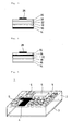
- FIG. 1 is a schematic representation showing an example of a voltage controlled oscillator using a resonator of the present invention.
- a voltage controlled oscillator 10 includes a multilayer substrate 12.
- a first grounding conductor layer 14 is formed on a reverse side of the multilayer substrate 12 as shown in Fig. 2.
- a first dielectric layer 16 is laminated on the first grounding conductor layer 14.
- a strip line layer 18 is formed on the first grounding conductor layer 16.
- a strip line 20 is formed, for example, in a U-shaped manner on the strip line layer 18.
- a second dielectric layer 22 is laminated on the strip line layer 18.
- a second grounding conductor layer 24 is laminated on the second dielectric layer 22.
- a third dielectric layer 26 is laminated on the second grounding conductor layer 24.
- a microstrip line 28 is formed on the third dielectric layer 26. One end of the microstrip line 28 is formed on a part corresponding to one end of the strip line 20.
- a through hole 30 is formed in the second dielectric layer 22, the second grounding conductor layer 24, and the third dielectric layer 26.
- the strip line 20 is connected to the microstrip line 28 via the through hole 30 to form a resonator.
- a portion 32 of the second grounding conductor layer 24 facing the microstrip line 28 is removed, and the microstrip line 28 and the first grounding conductor layer 14 are disposed facing each other via the dielectric layers 16, 22, 26.
- a plurality of electronic parts 34 are mounted on the surface with the microstrip line 28 formed thereon to form a circuit. This circuit is connected to the resonator to constitute the voltage controlled oscillator 10.
- the multilayer substrate 12 is manufactured by printing an electrode paste on a dielectric ceramic green sheet in the shape of each conductor layer, strip line, and microstrip line, and then laminating and baking the electrode paste.
- the electrode paste printed part forming the second grounding conductor layer 24 the portion 32 facing the microstrip line 28 is formed by not printing the electrode paste thereat.
- the first grounding conductor layer 14, the first dielectric layer 16, the strip line 20 formed on the strip line layer 18, the second dielectric layer 22, and the second grounding conductor layer 24 form a strip line resonator
- the first grounding conductor layer 16, the three dielectric layers 16, 22, 26, and the microstrip line 28 form a microstrip line resonator.
- a single resonator is formed by connecting the strip line resonator to the microstrip line resonator.
- one resonator comprises one strip line resonator and one microstrip line resonator, and thus, the area of the microstrip line 28 can be reduced compared with a case where the resonator comprises only microstrip lines.
- the multilayer substrate 12 can be reduced in size.
- the frequency of the resonator can be adjusted by cutting the microstrip line 28 formed on the surface of the multilayer substrate 12.
- the portion 32 facing the microstrip line 28 of the second grounding conductor layer 24 inside the multilayer substrate 12 is removed, and thus, the microstrip line 28 and the first grounding conductor layer 14 are facing each other as shown in Fig. 3, and the dielectric layers 16, 22, 26 therebetween are thick.
- the Q factor can be improved compared with a case where the microstrip line 28 and the second grounding conductor layer 24 are facing each other as shown in Fig. 4.
- the structure of the multilayer substrate 12 is not limited to the structure shown in Figs. 1 and 2, and other conductor layer may be formed thereon. Also, in such a case, the space between the microstrip line 28 and the conductor layer facing it can be increased by removing a portion facing the microstrip line of the inside conductor layer.
- the conductor layer facing the microstrip line 28 is not limited to the first grounding conductor layer 14; however, the microstrip line 28 may face a conductor layer inside the multilayer substrate 12, and the space between the microstrip line 28 and the conductor layer facing it may be determined according to a necessary characteristic.
- the area of the microstrip line on the surface of the multilayer substrate can be reduced by forming a resonator by connecting the strip line to the microstrip line, and thus the resonator can also be reduced in size. Further, the frequency of the resonator can be easily adjusted by cutting the microstrip line on the surface of the multilayer substrate. In addition, the space between the microstrip line and the conductor layer facing it can be increased by removing the portion, facing the microstrip line, of the conductor layer inside the multilayer substrate and the Q factor can be improved thereby.
Landscapes
- Engineering & Computer Science (AREA)
- Microelectronics & Electronic Packaging (AREA)
- Inductance-Capacitance Distribution Constants And Capacitance-Resistance Oscillators (AREA)
- Control Of Motors That Do Not Use Commutators (AREA)
Abstract
Description
Claims (2)
- A resonator comprising:wherein at least a portion (32), facing the microstrip line (28), of said conductor layer (24) closest to said microstrip line (28) is removed.a multilayer substrate (12) comprising: at least two conductor layers (14, 24) which include at least two grounding conductor layers (14, 24); and a plurality of dielectric layers (16, 22, 26) with one of said grounding conductor (14) layers formed on a reverse side thereof;a strip line (20) formed between two of the grounding conductor layers (14, 24);a microstrip line (28) formed on a surface of said multilayer substrate (12); anda through hole (30) formed in said dielectric layer (22) to connect said strip line (20) to said microstrip line (28),
- A resonator according to Claim 1, wherein a portion (32) of said conductor layer (24) formed inside said multilayer substrate (12) facing said microstrip line (28) is removed so that said grounding conductor layer (14) formed on a reverse side of said multilayer substrate (12) is facing said microstrip line (28).
Applications Claiming Priority (2)
| Application Number | Priority Date | Filing Date | Title |
|---|---|---|---|
| JP2000210015 | 2000-07-11 | ||
| JP2000210015A JP2002026654A (en) | 2000-07-11 | 2000-07-11 | Resonator |
Publications (3)
| Publication Number | Publication Date |
|---|---|
| EP1172882A2 true EP1172882A2 (en) | 2002-01-16 |
| EP1172882A3 EP1172882A3 (en) | 2003-07-02 |
| EP1172882B1 EP1172882B1 (en) | 2004-09-15 |
Family
ID=18706346
Family Applications (1)
| Application Number | Title | Priority Date | Filing Date |
|---|---|---|---|
| EP01116871A Expired - Lifetime EP1172882B1 (en) | 2000-07-11 | 2001-07-10 | Resonator |
Country Status (5)
| Country | Link |
|---|---|
| US (1) | US6924707B2 (en) |
| EP (1) | EP1172882B1 (en) |
| JP (1) | JP2002026654A (en) |
| KR (1) | KR100397741B1 (en) |
| DE (1) | DE60105505T2 (en) |
Cited By (2)
| Publication number | Priority date | Publication date | Assignee | Title |
|---|---|---|---|---|
| EP1536553A1 (en) * | 2003-11-26 | 2005-06-01 | Alps Electric Co., Ltd. | Voltage controlled oscillator |
| EP1484837A3 (en) * | 2003-06-04 | 2005-07-20 | Seiko Epson Corporation | Voltage-controlled oscillator |
Families Citing this family (2)
| Publication number | Priority date | Publication date | Assignee | Title |
|---|---|---|---|---|
| KR100922576B1 (en) * | 2007-12-06 | 2009-10-21 | 한국전자통신연구원 | Ultra high frequency transmission device to improve the transmission characteristics in the millimeter wave band |
| DE102018104687B4 (en) | 2018-03-01 | 2023-09-14 | Danfoss A/S | Valve attachment |
Family Cites Families (8)
| Publication number | Priority date | Publication date | Assignee | Title |
|---|---|---|---|---|
| JP3088021B2 (en) * | 1990-12-20 | 2000-09-18 | 株式会社村田製作所 | Voltage controlled oscillator |
| JP2662748B2 (en) | 1991-04-30 | 1997-10-15 | 株式会社村田製作所 | Oscillator |
| JP3141350B2 (en) * | 1992-05-29 | 2001-03-05 | 京セラ株式会社 | Adjusting the oscillation frequency of the oscillation circuit |
| JP3198634B2 (en) * | 1992-06-25 | 2001-08-13 | 株式会社村田製作所 | Oscillator frequency adjustment method |
| JPH06216614A (en) * | 1993-01-14 | 1994-08-05 | Casio Comput Co Ltd | Resonance frequency adjusting method for strip line |
| JPH0766628A (en) | 1993-08-30 | 1995-03-10 | Kyocera Corp | Voltage controlled oscillator |
| JPH07297637A (en) * | 1994-04-27 | 1995-11-10 | Kyocera Corp | Resonant circuit board |
| JP2001244741A (en) | 2000-02-29 | 2001-09-07 | Matsushita Electric Ind Co Ltd | Voltage controlled oscillator |
-
2000
- 2000-07-11 JP JP2000210015A patent/JP2002026654A/en active Pending
-
2001
- 2001-07-09 KR KR10-2001-0040855A patent/KR100397741B1/en not_active Expired - Fee Related
- 2001-07-10 EP EP01116871A patent/EP1172882B1/en not_active Expired - Lifetime
- 2001-07-10 US US09/901,746 patent/US6924707B2/en not_active Expired - Fee Related
- 2001-07-10 DE DE60105505T patent/DE60105505T2/en not_active Expired - Fee Related
Cited By (4)
| Publication number | Priority date | Publication date | Assignee | Title |
|---|---|---|---|---|
| EP1484837A3 (en) * | 2003-06-04 | 2005-07-20 | Seiko Epson Corporation | Voltage-controlled oscillator |
| US6980061B2 (en) | 2003-06-04 | 2005-12-27 | Seiko Epson Corporation | Voltage-controlled oscillator |
| EP1536553A1 (en) * | 2003-11-26 | 2005-06-01 | Alps Electric Co., Ltd. | Voltage controlled oscillator |
| US7142068B2 (en) | 2003-11-26 | 2006-11-28 | Alps Electric Co., Ltd. | Voltage controlled oscillator small in reduction of inductance and Q |
Also Published As
| Publication number | Publication date |
|---|---|
| KR20020006442A (en) | 2002-01-19 |
| US6924707B2 (en) | 2005-08-02 |
| DE60105505T2 (en) | 2005-09-29 |
| JP2002026654A (en) | 2002-01-25 |
| DE60105505D1 (en) | 2004-10-21 |
| US20020011903A1 (en) | 2002-01-31 |
| KR100397741B1 (en) | 2003-09-13 |
| EP1172882A3 (en) | 2003-07-02 |
| EP1172882B1 (en) | 2004-09-15 |
Similar Documents
| Publication | Publication Date | Title |
|---|---|---|
| US6046409A (en) | Multilayer microelectronic circuit | |
| EP1378958A1 (en) | Composite high frequency apparatus | |
| EP1439599B1 (en) | Waveguide-Type dielectric filter | |
| EP0785590A1 (en) | Composite high-frequency component | |
| EP1172882B1 (en) | Resonator | |
| JP2001230610A (en) | Stacked dielectric resonator | |
| JPH05206730A (en) | Voltage controlled oscillator and adjustment method of its oscillating frequency | |
| JPH06252612A (en) | Circuit board with built-in stripline | |
| JPH05152803A (en) | Dielectric filter | |
| JP2004172466A (en) | Electronic component | |
| JPH05160605A (en) | High frequency circuit parts | |
| JP2001326444A (en) | Chip component mounting board | |
| US7142068B2 (en) | Voltage controlled oscillator small in reduction of inductance and Q | |
| US8130062B2 (en) | Microstripline filter | |
| JP2732186B2 (en) | Manufacturing method of laminated dielectric filter | |
| JPH06283903A (en) | Dielectric filter | |
| JP2853480B2 (en) | Varactor loaded resonator | |
| JPH0936603A (en) | Antenna switch | |
| JP2000349506A (en) | Stripline filter | |
| JPH0878907A (en) | Multilayer dielectric filter | |
| JPH03187503A (en) | Multilayered substrate | |
| JPH11136001A (en) | Stacked stripline filter with improved frequency characteristics | |
| JPH05183307A (en) | Band width adjustment method for strip line filter | |
| JP2001237620A (en) | Laminated dielectric resonator | |
| JP2000022480A (en) | Laminated filter |
Legal Events
| Date | Code | Title | Description |
|---|---|---|---|
| PUAI | Public reference made under article 153(3) epc to a published international application that has entered the european phase |
Free format text: ORIGINAL CODE: 0009012 |
|
| 17P | Request for examination filed |
Effective date: 20010710 |
|
| AK | Designated contracting states |
Kind code of ref document: A2 Designated state(s): AT BE CH CY DE DK ES FI FR GB GR IE IT LI LU MC NL PT SE TR |
|
| AX | Request for extension of the european patent |
Free format text: AL;LT;LV;MK;RO;SI |
|
| PUAL | Search report despatched |
Free format text: ORIGINAL CODE: 0009013 |
|
| AK | Designated contracting states |
Designated state(s): AT BE CH CY DE DK ES FI FR GB GR IE IT LI LU MC NL PT SE TR |
|
| AX | Request for extension of the european patent |
Extension state: AL LT LV MK RO SI |
|
| GRAP | Despatch of communication of intention to grant a patent |
Free format text: ORIGINAL CODE: EPIDOSNIGR1 |
|
| AKX | Designation fees paid |
Designated state(s): DE FR GB |
|
| GRAS | Grant fee paid |
Free format text: ORIGINAL CODE: EPIDOSNIGR3 |
|
| GRAA | (expected) grant |
Free format text: ORIGINAL CODE: 0009210 |
|
| AK | Designated contracting states |
Kind code of ref document: B1 Designated state(s): DE FR GB |
|
| REG | Reference to a national code |
Ref country code: GB Ref legal event code: FG4D |
|
| REG | Reference to a national code |
Ref country code: IE Ref legal event code: FG4D |
|
| REF | Corresponds to: |
Ref document number: 60105505 Country of ref document: DE Date of ref document: 20041021 Kind code of ref document: P |
|
| PLBE | No opposition filed within time limit |
Free format text: ORIGINAL CODE: 0009261 |
|
| STAA | Information on the status of an ep patent application or granted ep patent |
Free format text: STATUS: NO OPPOSITION FILED WITHIN TIME LIMIT |
|
| ET | Fr: translation filed | ||
| 26N | No opposition filed |
Effective date: 20050616 |
|
| PGFP | Annual fee paid to national office [announced via postgrant information from national office to epo] |
Ref country code: DE Payment date: 20080717 Year of fee payment: 8 |
|
| PGFP | Annual fee paid to national office [announced via postgrant information from national office to epo] |
Ref country code: FR Payment date: 20080718 Year of fee payment: 8 |
|
| PGFP | Annual fee paid to national office [announced via postgrant information from national office to epo] |
Ref country code: GB Payment date: 20080716 Year of fee payment: 8 |
|
| GBPC | Gb: european patent ceased through non-payment of renewal fee |
Effective date: 20090710 |
|
| REG | Reference to a national code |
Ref country code: FR Ref legal event code: ST Effective date: 20100331 |
|
| PG25 | Lapsed in a contracting state [announced via postgrant information from national office to epo] |
Ref country code: FR Free format text: LAPSE BECAUSE OF NON-PAYMENT OF DUE FEES Effective date: 20090731 |
|
| PG25 | Lapsed in a contracting state [announced via postgrant information from national office to epo] |
Ref country code: GB Free format text: LAPSE BECAUSE OF NON-PAYMENT OF DUE FEES Effective date: 20090710 |
|
| PG25 | Lapsed in a contracting state [announced via postgrant information from national office to epo] |
Ref country code: DE Free format text: LAPSE BECAUSE OF NON-PAYMENT OF DUE FEES Effective date: 20100202 |