EP1172860A2 - Hemt device with a buffer to channel insert layer - Google Patents
Hemt device with a buffer to channel insert layer Download PDFInfo
- Publication number
- EP1172860A2 EP1172860A2 EP01116415A EP01116415A EP1172860A2 EP 1172860 A2 EP1172860 A2 EP 1172860A2 EP 01116415 A EP01116415 A EP 01116415A EP 01116415 A EP01116415 A EP 01116415A EP 1172860 A2 EP1172860 A2 EP 1172860A2
- Authority
- EP
- European Patent Office
- Prior art keywords
- layer
- channel
- disposing
- buffer layer
- lattice constant
- Prior art date
- Legal status (The legal status is an assumption and is not a legal conclusion. Google has not performed a legal analysis and makes no representation as to the accuracy of the status listed.)
- Withdrawn
Links
Images
Classifications
-
- H—ELECTRICITY
- H10—SEMICONDUCTOR DEVICES; ELECTRIC SOLID-STATE DEVICES NOT OTHERWISE PROVIDED FOR
- H10D—INORGANIC ELECTRIC SEMICONDUCTOR DEVICES
- H10D30/00—Field-effect transistors [FET]
- H10D30/40—FETs having zero-dimensional [0D], one-dimensional [1D] or two-dimensional [2D] charge carrier gas channels
- H10D30/47—FETs having zero-dimensional [0D], one-dimensional [1D] or two-dimensional [2D] charge carrier gas channels having two-dimensional [2D] charge carrier gas channels, e.g. nanoribbon FETs or high electron mobility transistors [HEMT]
- H10D30/471—High electron mobility transistors [HEMT] or high hole mobility transistors [HHMT]
- H10D30/473—High electron mobility transistors [HEMT] or high hole mobility transistors [HHMT] having confinement of carriers by multiple heterojunctions, e.g. quantum well HEMT
Definitions
- the present invention relates generally to High Electron Mobility Transistor (HEMT) devices and more particularly, to a HEMT device having an insert layer between the buffer layer and the channel.
- HEMT High Electron Mobility Transistor
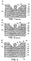
- FIGs. 1 & 2 show typical prior art indium phosphide (InP) based 10 and gallium arsenide (GaAs) 12 based HEMT devices.
- Each HEMT device 10, 12 comprises a buffer layer 14, 16 grown on a substrate 18, 20.
- a channel layer 22, 24 is grown on each buffer layer 14, 16 and a barrier layer 26, 28 is grown over each channel layer 22, 24.
- Cap layers 30, 32 are grown over the barrier layers 26, 28 and a portion of each cap layer 30, 32 is removed to form recesses 34, 36 in the cap layers 30, 32.
- a gate 38, 40 is positioned in each recess 34, 36, and source 42, 44 and drain 46, 48 contacts are deposited on either side of the gates 38, 40 on the cap layers 30, 32, respectively.
- the substrate 18 is fabricated of an InP material and the buffer layer 14 is fabricated of an indium aluminum arsenide (InAlAs) material.
- the channel 22 is fabricated of an indium gallium arsenide (InGaAs) material comprising greater than 52% of indium.
- the barrier layer 26 is fabricated of an InAlAs material and typically includes silicon (Si) planar doping 50 near the channel 22.
- the cap 30 is fabricated of an InGaAs material.
- the substrate 20 is fabricated of a GaAs material and the buffer layer 16 is fabricated of both a GaAs and aluminum gallium arsenide (AlGaAs) material where the GaAs material is near the substrate 20 and the AlGaAs material is near the channel 24.
- the channel 24 is fabricated of an InGaAs material and the barrier layer 28 is fabricated of an AlGaAs material.
- the barrier layer 28 typically includes a Si doping layer 52, and, the cap 32 is fabricated of a GaAs material.
- One disadvantage of prior art HEMT devices 10, 12 is that it is difficult to begin growth of the channels 22, 24 directly on the buffers 14, 16. This is primarily due to the large difference in lattice constants between the buffers 14, 16 and the channels 22, 24. This large difference in the lattice constants results in a rough interface 54, 56 between each buffer layer 14, 16 and the associated channels 22, 24. The rough interfaces 54, 56 can cause defects or traps between the buffer layers 14, 16 and the channels 22, 24 reducing the electrical performance of the associated HEMT device 10, 12.
- a second disadvantage of the prior art HEMT devices 10, 12 is that the performance of the HEMT device 10, 12 is very dependant on the cleanliness of the system in which the HEMT device 10, 12 is grown.
- HEMT devices 10, 12 are grown by methods such as molecular beam epitaxy (MBE) in a vacuum environment which is ideally free of impurities. Realistically however, it is extremely difficult and very expensive to provide a vacuum environment which is totally free of all impurities. This results in variability in the performance of the HEMT devices 10, 12 because the impurities, particular oxygen, incorporate into the buffer layers 14, 16 and can adversely effect the transport of electrons in the channels 22, 24.
- MBE molecular beam epitaxy
- the present invention provides a HEMT device and a method for fabricating a HEMT device having an insert layer between the buffer layer and the channel which reduces the channel's sensitivity to impurities in the deposition system and provides an easier interface upon which to grow the channel.
- the method comprises disposing a buffer layer having a lattice constant on a substrate.
- a channel having a lattice constant is disposed over the buffer layer; and, an insert layer having a lattice constant is disposed between the buffer layer and the channel with the lattice constant of the insert layer selected to be intermediate the lattice constant of the buffer layer and the channel.
- a barrier layer is disposed on the channel and a cap layer is disposed on the barrier layer.
- a recess is formed in the cap layer exposing the barrier layer and a gate is positioned on the exposed portion of the barrier layer.
- a source and the drain are positioned on the cap.
- the present invention provides a HEMT device having a gate, a source and a drain.
- a buffer layer having a lattice constant is disposed on a substrate.
- An insert layer having a lattice constant greater than the lattice constant of the buffer layer is disposed on the buffer layer.
- a channel having a lattice constant greater than the lattice constant of the insert layer is disposed on the insert layer.
- a barrier layer is disposed over the channel layer and, a cap is deposited on the barrier layer.
- the gate is disposed on a portion of the barrier layer through a recess in the cap and, a source and a drain are disposed on the cap.
- the present invention provides a HEMT device 60 which addresses and overcomes the disadvantages of the prior art by providing an insert layer 62 between the buffer layer 64 and the channel 66.
- the buffer layer 64 is disposed on the substrate 68 and the insert layer 62 is disposed on the buffer layer 64.
- the channel 66 is disposed on the insert layer 62 and a barrier layer 70 is disposed on the channel 66.
- the barrier layer 70 preferably includes a doping layer 72 near the channel 66 where the doping layer 72 is preferably a Si planar doping layer.
- a cap 74 is disposed on the barrier layer 70.
- a gate 76 is disposed on the barrier layer 70 through a recess 78 in the cap layer 74, and a drain 79 and a source 80 are disposed on the cap 74.
- the layers 62-70 & 74, gate 76, drain 78 and source 80 are preferably disposed by a depositing method or a growth method known to one skilled in the art.
- the insert layer 62 is a lattice constant transition layer which, when grown on the buffer layer 64, provides a surface 82 having a larger lattice constant for the channel 66 to be deposited on than that provided by the buffer layer 64.
- the material for the insert layer 62 is selected so that the lattice constant of the insert layer 62 is between the lattice constant of the buffer layer 64 and the lattice constant of the channel 66.
- the material for the insert layer 62 is selected so that the lattice constant of the insert layer 62 is approximately halfway between the lattice constants of the buffer layer 64 and the channel 66.
- Selecting the material for the insert layer 62 to have a lattice constant between that of the buffer layer 64 and the channel 66 provides a surface 82 with a lattice constant closer to that of the channel 66 than the lattice constant provided by the buffer layer 64.
- the channel 66 can be grown with better crystal quality when grown on the larger lattice constant of the insert layer 62 than on the lattice constant of the buffer layer 64.
- CBE conduction band energy
- the insert layer 62 also provides a surface 82 which is less prone to impurities during a deposition or growth process than the surface 84 of the buffer layer 64.
- layers 62-70 & 74 are typically disposed by a deposition system, such as an MBE system. As such, the cleanliness of the deposition system can vary significantly and the defects in the buffer layer 64 can vary significantly with minor effect on the performance of the channel 66.
- the surface 82 of the insert layer 62 is less susceptible to impurities in an MBE vacuum environment because the insert layer 62 either does not contain aluminum or has a lower aluminum content than the buffer layer 64. As such, the insert layer 62 is much less susceptible to the impurities in the deposition system. This results in more repeatable channel characteristics from one HEMT device to another HEMT device in a production environment.
- the insert layer 42 is limited to a thickness of about 1-10 nm since after about 10 nm, the insert layer 42 begins to adversely effect the ability to control the electrons in the channel 46 which can decrease the electrical characteristics of the channel 46.
- a HEMT device is a controlled electron device and, as such, it is important to control the flow of the electrons in the channel 46. It is easier to control the electrons if they are concentrated together in a narrower channel. Simulations have shown that an unacceptable loss of control of the electrons in the channel 46 exists once the insert layer 42 is wider than about 10 nm.
- the exact material selected for the insert layer 62 is dependent on the materials used for the buffer layer 64 and the channel 66.
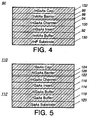
- the buffer layer 92 is fabricated of an InAlAs material and the channel 94 is fabricated of an InGaAs material.
- the barrier layer 96 is fabricated of an InAlAs material and includes a Si planar doping layer 98 which is deposited near the channel 94.
- the gate, source and drain of a HEMT device are typically omitted from cross-sectional views of a HEMT device. In accordance with this practice, the gates, sources and drains will not be shown in subsequent cross-sectional drawings of HEMT devices.
- each HEMT device includes a gate, a source and a drain.
- the insert layer 100 is preferably fabricated of an InGaAs material comprising no more than 53% Indium. This InGaAs material has a lattice constant which is between that of the InAlAs buffer layer 92 and the InGaAs channel 94.
- the buffer layer 112 is comprised of GaAs/AlGaAs materials with the AlGaAs portion 114 of the buffer layer 112 deposited nearest the insert layer 116 and the GaAs portion 118 of the buffer layer 112 deposited nearest the substrate 120.
- the channel 122 is fabricated of an InGaAs material and the barrier layer 124 is fabricated of an AlGaAs material and includes a Si planar doping layer 126 near the channel 122.
- the insert 116 is preferably fabricated of a GaAs material having a lattice constant which is greater than the lattice constant of the AlGaAs portion 114 of the buffer layer 112 and smaller than the lattice constant of the InGaAs material of the channel 122.
- the buffer layer 92 was fabricated of an InAlAs material to a thickness of 300 nm.
- the insert layer 100 was fabricated of 10 nm thick InGaAs material which was lattice matched to the InP substrate 130.
- the channel 94 was fabricated of 20 nm thick InGaAs material which comprised greater than 53% Indium.
- the barrier layer 96 was fabricated of 28 nm thick InAlAs material which included a Si planar doping layer 98 near the channel 94.
- the cap 132 was fabricated of 20 nm thick InGaAs material.
- the transconductance and gain of this fabricated HEMT device were measured at a frequency of 190 GHz.
- the fabricated HEMT device provided better confinement of the electrons in the channel 94 and measured an approximately 15% improvement in the transconductance which translates to a 2.8 dB increase in gain.
- the present invention is not limited to the structures and figures shown and described hereinabove but can be practiced with any HEMT device in which the lattice constant of the buffer layer is lower than the lattice constant of the channel. It will be appreciated that many variations of the invention are possible and the invention is not limited only by the claims which follow.
Landscapes
- Junction Field-Effect Transistors (AREA)
Abstract
A HEMT device having an insert layer between the buffer layer and the
channel. The HEMT device comprises a buffer layer having a lattice constant and
being disposed on a substrate. A channel having a lattice constant is disposed over
the buffer layer and an insert layer having a lattice constant is disposed between the
buffer layer and the channel with the lattice constant of the insert layer being
intermediate the lattice constant of the buffer layer and the channel. The insert
layer provides for a HEMT device having a decreased sensitivity to impurities in the
deposition system and provides for an easier interface upon which to grow the
channel.
Description
- The present invention relates generally to High Electron Mobility Transistor (HEMT) devices and more particularly, to a HEMT device having an insert layer between the buffer layer and the channel.
- FIGs. 1 & 2 show typical prior art indium phosphide (InP) based 10 and gallium arsenide (GaAs) 12 based HEMT devices. Each
HEMT device buffer layer substrate channel layer buffer layer barrier layer channel layer Cap layers barrier layers cap layer recesses cap layers gate recess source drain gates cap layers - For the typical prior art
InP HEMT device 10 of FIG. 1, thesubstrate 18 is fabricated of an InP material and thebuffer layer 14 is fabricated of an indium aluminum arsenide (InAlAs) material. Thechannel 22 is fabricated of an indium gallium arsenide (InGaAs) material comprising greater than 52% of indium. Thebarrier layer 26 is fabricated of an InAlAs material and typically includes silicon (Si)planar doping 50 near thechannel 22. Thecap 30 is fabricated of an InGaAs material. - For the typical prior art GaAs HEMT
device 12 of FIG. 2, thesubstrate 20 is fabricated of a GaAs material and thebuffer layer 16 is fabricated of both a GaAs and aluminum gallium arsenide (AlGaAs) material where the GaAs material is near thesubstrate 20 and the AlGaAs material is near thechannel 24. Thechannel 24 is fabricated of an InGaAs material and thebarrier layer 28 is fabricated of an AlGaAs material. Thebarrier layer 28 typically includes aSi doping layer 52, and, thecap 32 is fabricated of a GaAs material. - One disadvantage of prior
art HEMT devices channels buffers buffers channels rough interface buffer layer associated channels rough interfaces buffer layers channels HEMT device - A second disadvantage of the prior
art HEMT devices HEMT device HEMT device HEMT devices HEMT devices buffer layers channels - What is needed therefore is a method for producing a HEMT device which provides for ease of growth of the channel and additionally is less sensitive to imperfections in the growth process than prior art HEMT devices.
- The proceeding and other shortcomings of the prior art are addressed and overcome by the present invention which provides a HEMT device and a method for fabricating a HEMT device having an insert layer between the buffer layer and the channel which reduces the channel's sensitivity to impurities in the deposition system and provides an easier interface upon which to grow the channel.
- The method comprises disposing a buffer layer having a lattice constant on a substrate. A channel having a lattice constant is disposed over the buffer layer; and, an insert layer having a lattice constant is disposed between the buffer layer and the channel with the lattice constant of the insert layer selected to be intermediate the lattice constant of the buffer layer and the channel. A barrier layer is disposed on the channel and a cap layer is disposed on the barrier layer. A recess is formed in the cap layer exposing the barrier layer and a gate is positioned on the exposed portion of the barrier layer. To complete the HEMT device, a source and the drain are positioned on the cap.
- In a second aspect, the present invention provides a HEMT device having a gate, a source and a drain. A buffer layer having a lattice constant is disposed on a substrate. An insert layer having a lattice constant greater than the lattice constant of the buffer layer is disposed on the buffer layer. A channel having a lattice constant greater than the lattice constant of the insert layer is disposed on the insert layer. A barrier layer is disposed over the channel layer and, a cap is deposited on the barrier layer. To complete the HEMT device, the gate is disposed on a portion of the barrier layer through a recess in the cap and, a source and a drain are disposed on the cap.
- Reference is now made to the detailed description of the preferred embodiments, illustrated in the accompanying drawings, in which:
- FIG 1 shows a cross-sectional view of an InP based HEMT device in accordance with the prior art;
- FIG. 2 shows a cross-sectional view of a GaAs based HEMT device in accordance with the prior art;
- FIG. 3 shows a cross-sectional view of a HEMT device having an insert layer in accordance with a first embodiment of the present invention;
- FIG. 4 shows a cross-sectional view of a portion of a InP-based HEMT device with a InGaAs insert layer in accordance with a second embodiment of the present invention; and,
- FIG. 5 shows a cross-sectional view of a portion of an GaAs-based HEMT device having a GaAs insert layer in accordance with a third embodiment of the present invention.
-
- Referring to FIG. 3, the present invention provides a
HEMT device 60 which addresses and overcomes the disadvantages of the prior art by providing aninsert layer 62 between thebuffer layer 64 and thechannel 66. Thebuffer layer 64 is disposed on thesubstrate 68 and theinsert layer 62 is disposed on thebuffer layer 64. Thechannel 66 is disposed on theinsert layer 62 and abarrier layer 70 is disposed on thechannel 66. Thebarrier layer 70 preferably includes adoping layer 72 near thechannel 66 where thedoping layer 72 is preferably a Si planar doping layer. Acap 74 is disposed on thebarrier layer 70. To complete the HEMTdevice 60, agate 76 is disposed on thebarrier layer 70 through arecess 78 in thecap layer 74, and adrain 79 and asource 80 are disposed on thecap 74. The layers 62-70 & 74,gate 76,drain 78 andsource 80 are preferably disposed by a depositing method or a growth method known to one skilled in the art. - The
insert layer 62 is a lattice constant transition layer which, when grown on thebuffer layer 64, provides asurface 82 having a larger lattice constant for thechannel 66 to be deposited on than that provided by thebuffer layer 64. The material for theinsert layer 62 is selected so that the lattice constant of theinsert layer 62 is between the lattice constant of thebuffer layer 64 and the lattice constant of thechannel 66. Preferably, the material for theinsert layer 62 is selected so that the lattice constant of theinsert layer 62 is approximately halfway between the lattice constants of thebuffer layer 64 and thechannel 66. Selecting the material for theinsert layer 62 to have a lattice constant between that of thebuffer layer 64 and thechannel 66 provides asurface 82 with a lattice constant closer to that of thechannel 66 than the lattice constant provided by thebuffer layer 64. As such, thechannel 66 can be grown with better crystal quality when grown on the larger lattice constant of theinsert layer 62 than on the lattice constant of thebuffer layer 64. - In addition to providing a better surface to grow the
channel 66 upon, selecting a material for theinsert layer 62 to have a lattice constant between that of thebuffer layer 64 and thechannel layer 66 results in theinsert layer 62 having a conduction band energy (CBE) which is greater than the CBE of thechannel 66. Conduction band energy (CBE) is known to define how the electrons in theHEMT device 60 will respond to a voltage applied across thedevice 60. In aHEMT device 60, the electrons will move towards the layer having the lowest CBE. To provide aHEMT device 60 in which most of the electrons flow in thechannel 66, the CBE of thechannel 66 must be lower than the CBE of theinsert layer 62. As such, the present invention provides for the desirable property that most of the electrons in theHEMT device 60 will flow in thechannel 66. - The
insert layer 62 also provides asurface 82 which is less prone to impurities during a deposition or growth process than thesurface 84 of thebuffer layer 64. As previously mentioned, layers 62-70 & 74 are typically disposed by a deposition system, such as an MBE system. As such, the cleanliness of the deposition system can vary significantly and the defects in thebuffer layer 64 can vary significantly with minor effect on the performance of thechannel 66. Thesurface 82 of theinsert layer 62 is less susceptible to impurities in an MBE vacuum environment because theinsert layer 62 either does not contain aluminum or has a lower aluminum content than thebuffer layer 64. As such, theinsert layer 62 is much less susceptible to the impurities in the deposition system. This results in more repeatable channel characteristics from one HEMT device to another HEMT device in a production environment. - For the preferred embodiment of the invention, the
insert layer 42 is limited to a thickness of about 1-10 nm since after about 10 nm, theinsert layer 42 begins to adversely effect the ability to control the electrons in thechannel 46 which can decrease the electrical characteristics of thechannel 46. A HEMT device is a controlled electron device and, as such, it is important to control the flow of the electrons in thechannel 46. It is easier to control the electrons if they are concentrated together in a narrower channel. Simulations have shown that an unacceptable loss of control of the electrons in thechannel 46 exists once theinsert layer 42 is wider than about 10 nm. - The exact material selected for the
insert layer 62 is dependent on the materials used for thebuffer layer 64 and thechannel 66. For example, referring to FIG. 4, for an InP basedHEMT device 90, thebuffer layer 92 is fabricated of an InAlAs material and thechannel 94 is fabricated of an InGaAs material. Thebarrier layer 96 is fabricated of an InAlAs material and includes a Siplanar doping layer 98 which is deposited near thechannel 94. Note that the gate, source and drain of a HEMT device are typically omitted from cross-sectional views of a HEMT device. In accordance with this practice, the gates, sources and drains will not be shown in subsequent cross-sectional drawings of HEMT devices. However, it is understood that each HEMT device includes a gate, a source and a drain. ForInP HEMT device 90 shown in FIG. 4, theinsert layer 100 is preferably fabricated of an InGaAs material comprising no more than 53% Indium. This InGaAs material has a lattice constant which is between that of theInAlAs buffer layer 92 and theInGaAs channel 94. - As another example, referring to FIG. 5, for a GaAs-based
HEMT device 110, thebuffer layer 112 is comprised of GaAs/AlGaAs materials with theAlGaAs portion 114 of thebuffer layer 112 deposited nearest theinsert layer 116 and theGaAs portion 118 of thebuffer layer 112 deposited nearest thesubstrate 120. Thechannel 122 is fabricated of an InGaAs material and thebarrier layer 124 is fabricated of an AlGaAs material and includes a Siplanar doping layer 126 near thechannel 122. For thisGaAs HEMT device 110, theinsert 116 is preferably fabricated of a GaAs material having a lattice constant which is greater than the lattice constant of theAlGaAs portion 114 of thebuffer layer 112 and smaller than the lattice constant of the InGaAs material of thechannel 122. - An InP based HEMT device having an insert layer in accordance with the present invention was fabricated and tested. Referring back to FIG. 4, the
buffer layer 92 was fabricated of an InAlAs material to a thickness of 300 nm. Theinsert layer 100 was fabricated of 10 nm thick InGaAs material which was lattice matched to theInP substrate 130. Thechannel 94 was fabricated of 20 nm thick InGaAs material which comprised greater than 53% Indium. Thebarrier layer 96 was fabricated of 28 nm thick InAlAs material which included a Siplanar doping layer 98 near thechannel 94. Thecap 132 was fabricated of 20 nm thick InGaAs material. The transconductance and gain of this fabricated HEMT device were measured at a frequency of 190 GHz. When compared to a HEMT device without an insert, the fabricated HEMT device provided better confinement of the electrons in thechannel 94 and measured an approximately 15% improvement in the transconductance which translates to a 2.8 dB increase in gain. - As will be appreciated by one skilled in the art, the present invention is not limited to the structures and figures shown and described hereinabove but can be practiced with any HEMT device in which the lattice constant of the buffer layer is lower than the lattice constant of the channel. It will be appreciated that many variations of the invention are possible and the invention is not limited only by the claims which follow.
Claims (11)
- A method for fabricating a HEMT device comprising the steps of:disposing a buffer layer having a lattice constant on a substrate;disposing an insert layer having a lattice constant greater than the lattice constant of the buffer layer over said buffer layer;disposing a channel having a lattice constant greater than the lattice constant of the insert layer on the insert layer;disposing a barrier layer over said channel layer;disposing a cap on said barrier layer;exposing a portion of said barrier layer;disposing a gate on the exposed portion of the barrier layer; and,disposing a gate and a source on said cap.
- The method of claim 1, wherein exposing a portion of said barrier layer comprises removing a portion of said cap to expose a portion of said barrier layer.
- The method of claim 1, wherein disposing a buffer layer comprises disposing a buffer layer having a lattice constant and a conduction band energy on a substrate;disposing an insert layer comprises disposing an insert layer having a lattice constant greater than that of the buffer layer and a conduction band energy less than that of the buffer layer on said buffer layer; and,disposing a channel comprises disposing a channel having a lattice constant greater than the lattice constant of the insert layer and a conduction band energy less than the conduction band energy of the insert layer over the insert layer.
- The method of claim 1, wherein disposing a buffer layer comprises disposing a buffer layer fabricated of an InAlAs material having a lattice constant on a InP substrate;disposing an insert layer comprises disposing an insert layer fabricated of InGaAs material lattice matched to said substrate on said buffer layer; and,disposing a channel comprises disposing a channel of InGaAs material over said buffer layer.
- The method of claim 1, wherein disposing a buffer layer comprises disposing a buffer layer fabricated of a GaAs/AlGaAs material on a GaAs substrate;disposing an insert layer comprises disposing an insert layer fabricated of GaAs material lattice matched to said substrate on said buffer layer; and,disposing a channel comprises disposing a channel comprises InGaAs having greater than 52% indium over said buffer layer.
- A high electron mobility transistor (HEMT) device having a gate, source and drain comprising:a buffer layer having a lattice constant and being disposed on a substrate;an insert layer having a lattice constant greater than the lattice constant of the buffer layer and being disposed on said buffer layer;a channel having a lattice constant greater than the lattice constant of insert layer and being disposed on said insert layer;a barrier layer disposed over said channel; and,a cap disposed over said barrier layer, wherein said gate is positioned on said barrier layer and said source and drain are positioned on said cap.
- A HEMT device as in claim 6, wherein said gate is positioned on said barrier layer through a recess formed in said cap.
- A HEMT device as in claim 6, wherein said buffer layer, channel and insert layer each have a conduction band energy, the conduction band energy of the insert layer being between that of the buffer layer and the channel.
- A HEMT device as in claim 6, wherein said buffer layer comprises an InAlAs material, said channel comprises an InGaAs material, said insert layer comprises InGaAs material and said substrate comprise InP material.
- A HEMT device as in claim 6, wherein said insert layer is fabricated of a material which is lattice matched to said substrate.
- A HEMT device as in claim 6, wherein said buffer layer comprises an AlGaAs material, said channel comprises a GaAs/InGaAs material, said insert layer comprises a GaAs material; and, said substrate comprises a GaAs material.
Applications Claiming Priority (2)
| Application Number | Priority Date | Filing Date | Title |
|---|---|---|---|
| US616351 | 1984-06-01 | ||
| US61635100A | 2000-07-14 | 2000-07-14 |
Publications (1)
| Publication Number | Publication Date |
|---|---|
| EP1172860A2 true EP1172860A2 (en) | 2002-01-16 |
Family
ID=24469060
Family Applications (1)
| Application Number | Title | Priority Date | Filing Date |
|---|---|---|---|
| EP01116415A Withdrawn EP1172860A2 (en) | 2000-07-14 | 2001-07-06 | Hemt device with a buffer to channel insert layer |
Country Status (2)
| Country | Link |
|---|---|
| EP (1) | EP1172860A2 (en) |
| JP (1) | JP2002050641A (en) |
Families Citing this family (1)
| Publication number | Priority date | Publication date | Assignee | Title |
|---|---|---|---|---|
| CN102881715B (en) * | 2012-07-06 | 2016-04-13 | 电子科技大学 | A kind of high-frequency low noise gallium nitride based transistor structure with high electron mobility |
-
2001
- 2001-07-06 EP EP01116415A patent/EP1172860A2/en not_active Withdrawn
- 2001-07-16 JP JP2001215682A patent/JP2002050641A/en active Pending
Also Published As
| Publication number | Publication date |
|---|---|
| JP2002050641A (en) | 2002-02-15 |
Similar Documents
| Publication | Publication Date | Title |
|---|---|---|
| US6515316B1 (en) | Partially relaxed channel HEMT device | |
| US6797994B1 (en) | Double recessed transistor | |
| US6177685B1 (en) | Nitride-type III-V HEMT having an InN 2DEG channel layer | |
| US6489639B1 (en) | High electron mobility transistor | |
| JP2676442B2 (en) | Heterojunction field effect transistor and manufacturing method thereof | |
| EP0381396A1 (en) | Compound semiconductor devices | |
| WO2001011695A1 (en) | Double recessed transistor | |
| JP3376078B2 (en) | High electron mobility transistor | |
| JP2536523B2 (en) | Method for manufacturing semiconductor device | |
| US6919589B2 (en) | HEMT with a graded InGaAlP layer separating ohmic and Schottky contacts | |
| US5104825A (en) | Method of producing a semiconductor device | |
| US5322808A (en) | Method of fabricating inverted modulation-doped heterostructure | |
| JP2620901B2 (en) | GaAs heterostructure with stress compensation layer | |
| US5148245A (en) | Semiconductor device having a selectively doped heterostructure | |
| JPH0684957A (en) | High electron mobility field effect semiconductor device | |
| US5381027A (en) | Semiconductor device having a heterojunction and a two dimensional gas as an active layer | |
| US5466955A (en) | Field effect transistor having an improved transistor characteristic | |
| CA2070756C (en) | Field-effect transistor | |
| JP3447438B2 (en) | Field effect transistor | |
| JP2530496B2 (en) | Semiconductor heterostructure and manufacturing method thereof | |
| JPH0684959A (en) | High electron mobility field effect semiconductor device | |
| JP2002050641A (en) | HEMT device having insertion layer between buffer layer and channel | |
| JPH0574819A (en) | Compound semiconductor device | |
| JPH088354B2 (en) | Heterojunction field effect transistor | |
| JPH03211839A (en) | Compound semiconductor device and method of manufacturing the same |
Legal Events
| Date | Code | Title | Description |
|---|---|---|---|
| PUAI | Public reference made under article 153(3) epc to a published international application that has entered the european phase |
Free format text: ORIGINAL CODE: 0009012 |
|
| AK | Designated contracting states |
Kind code of ref document: A2 Designated state(s): AT BE CH CY DE DK ES FI FR GB GR IE IT LI LU MC NL PT SE TR |
|
| AX | Request for extension of the european patent |
Free format text: AL;LT;LV;MK;RO;SI |
|
| STAA | Information on the status of an ep patent application or granted ep patent |
Free format text: STATUS: THE APPLICATION HAS BEEN WITHDRAWN |
|
| 18W | Application withdrawn |
Withdrawal date: 20020114 |