EP1170786B1 - Silicon-on-insulator (SOI) semiconductor structure - Google Patents
Silicon-on-insulator (SOI) semiconductor structure Download PDFInfo
- Publication number
- EP1170786B1 EP1170786B1 EP01114983.8A EP01114983A EP1170786B1 EP 1170786 B1 EP1170786 B1 EP 1170786B1 EP 01114983 A EP01114983 A EP 01114983A EP 1170786 B1 EP1170786 B1 EP 1170786B1
- Authority
- EP
- European Patent Office
- Prior art keywords
- layer
- silicon
- trench
- insulator
- capacitor
- Prior art date
- Legal status (The legal status is an assumption and is not a legal conclusion. Google has not performed a legal analysis and makes no representation as to the accuracy of the status listed.)
- Expired - Lifetime
Links
- 239000012212 insulator Substances 0.000 title claims description 44
- 239000004065 semiconductor Substances 0.000 title claims description 30
- 239000000758 substrate Substances 0.000 claims description 60
- 239000003990 capacitor Substances 0.000 claims description 51
- XUIMIQQOPSSXEZ-UHFFFAOYSA-N Silicon Chemical compound [Si] XUIMIQQOPSSXEZ-UHFFFAOYSA-N 0.000 claims description 33
- 229910052710 silicon Inorganic materials 0.000 claims description 33
- 239000010703 silicon Substances 0.000 claims description 33
- VYPSYNLAJGMNEJ-UHFFFAOYSA-N Silicium dioxide Chemical compound O=[Si]=O VYPSYNLAJGMNEJ-UHFFFAOYSA-N 0.000 claims description 16
- 229910052581 Si3N4 Inorganic materials 0.000 claims description 13
- 239000000377 silicon dioxide Substances 0.000 claims description 8
- 235000012239 silicon dioxide Nutrition 0.000 claims description 5
- 238000000034 method Methods 0.000 description 19
- HQVNEWCFYHHQES-UHFFFAOYSA-N silicon nitride Chemical compound N12[Si]34N5[Si]62N3[Si]51N64 HQVNEWCFYHHQES-UHFFFAOYSA-N 0.000 description 10
- 230000015572 biosynthetic process Effects 0.000 description 9
- 230000000873 masking effect Effects 0.000 description 9
- 239000000463 material Substances 0.000 description 5
- 238000005229 chemical vapour deposition Methods 0.000 description 4
- 238000005530 etching Methods 0.000 description 4
- 229910021420 polycrystalline silicon Inorganic materials 0.000 description 4
- 239000004020 conductor Substances 0.000 description 3
- 238000004519 manufacturing process Methods 0.000 description 3
- 229910052751 metal Inorganic materials 0.000 description 3
- 239000002184 metal Substances 0.000 description 3
- 229920005591 polysilicon Polymers 0.000 description 3
- 230000008878 coupling Effects 0.000 description 2
- 238000010168 coupling process Methods 0.000 description 2
- 238000005859 coupling reaction Methods 0.000 description 2
- 239000003989 dielectric material Substances 0.000 description 2
- 208000032750 Device leakage Diseases 0.000 description 1
- NRTOMJZYCJJWKI-UHFFFAOYSA-N Titanium nitride Chemical compound [Ti]#N NRTOMJZYCJJWKI-UHFFFAOYSA-N 0.000 description 1
- 229910021417 amorphous silicon Inorganic materials 0.000 description 1
- IVHJCRXBQPGLOV-UHFFFAOYSA-N azanylidynetungsten Chemical compound [W]#N IVHJCRXBQPGLOV-UHFFFAOYSA-N 0.000 description 1
- 239000011248 coating agent Substances 0.000 description 1
- 238000000576 coating method Methods 0.000 description 1
- 239000013078 crystal Substances 0.000 description 1
- 230000003247 decreasing effect Effects 0.000 description 1
- 238000000151 deposition Methods 0.000 description 1
- 230000008021 deposition Effects 0.000 description 1
- 238000005137 deposition process Methods 0.000 description 1
- -1 however Substances 0.000 description 1
- 239000011810 insulating material Substances 0.000 description 1
- 238000002955 isolation Methods 0.000 description 1
- 150000002739 metals Chemical class 0.000 description 1
- 238000000059 patterning Methods 0.000 description 1
- 229920002120 photoresistant polymer Polymers 0.000 description 1
- 238000005498 polishing Methods 0.000 description 1
- 238000003860 storage Methods 0.000 description 1
- 239000000126 substance Substances 0.000 description 1
- MZLGASXMSKOWSE-UHFFFAOYSA-N tantalum nitride Chemical compound [Ta]#N MZLGASXMSKOWSE-UHFFFAOYSA-N 0.000 description 1
Images


Classifications
-
- H—ELECTRICITY
- H01—ELECTRIC ELEMENTS
- H01L—SEMICONDUCTOR DEVICES NOT COVERED BY CLASS H10
- H01L27/00—Devices consisting of a plurality of semiconductor or other solid-state components formed in or on a common substrate
- H01L27/02—Devices consisting of a plurality of semiconductor or other solid-state components formed in or on a common substrate including semiconductor components specially adapted for rectifying, oscillating, amplifying or switching and having at least one potential-jump barrier or surface barrier; including integrated passive circuit elements with at least one potential-jump barrier or surface barrier
- H01L27/12—Devices consisting of a plurality of semiconductor or other solid-state components formed in or on a common substrate including semiconductor components specially adapted for rectifying, oscillating, amplifying or switching and having at least one potential-jump barrier or surface barrier; including integrated passive circuit elements with at least one potential-jump barrier or surface barrier the substrate being other than a semiconductor body, e.g. an insulating body
- H01L27/13—Devices consisting of a plurality of semiconductor or other solid-state components formed in or on a common substrate including semiconductor components specially adapted for rectifying, oscillating, amplifying or switching and having at least one potential-jump barrier or surface barrier; including integrated passive circuit elements with at least one potential-jump barrier or surface barrier the substrate being other than a semiconductor body, e.g. an insulating body combined with thin-film or thick-film passive components
-
- H—ELECTRICITY
- H01—ELECTRIC ELEMENTS
- H01L—SEMICONDUCTOR DEVICES NOT COVERED BY CLASS H10
- H01L29/00—Semiconductor devices adapted for rectifying, amplifying, oscillating or switching, or capacitors or resistors with at least one potential-jump barrier or surface barrier, e.g. PN junction depletion layer or carrier concentration layer; Details of semiconductor bodies or of electrodes thereof ; Multistep manufacturing processes therefor
- H01L29/66—Types of semiconductor device ; Multistep manufacturing processes therefor
- H01L29/66007—Multistep manufacturing processes
- H01L29/66075—Multistep manufacturing processes of devices having semiconductor bodies comprising group 14 or group 13/15 materials
- H01L29/66083—Multistep manufacturing processes of devices having semiconductor bodies comprising group 14 or group 13/15 materials the devices being controllable only by variation of the electric current supplied or the electric potential applied, to one or more of the electrodes carrying the current to be rectified, amplified, oscillated or switched, e.g. two-terminal devices
- H01L29/66181—Conductor-insulator-semiconductor capacitors, e.g. trench capacitors
-
- H—ELECTRICITY
- H01—ELECTRIC ELEMENTS
- H01L—SEMICONDUCTOR DEVICES NOT COVERED BY CLASS H10
- H01L21/00—Processes or apparatus adapted for the manufacture or treatment of semiconductor or solid state devices or of parts thereof
- H01L21/70—Manufacture or treatment of devices consisting of a plurality of solid state components formed in or on a common substrate or of parts thereof; Manufacture of integrated circuit devices or of parts thereof
- H01L21/71—Manufacture of specific parts of devices defined in group H01L21/70
- H01L21/76—Making of isolation regions between components
- H01L21/762—Dielectric regions, e.g. EPIC dielectric isolation, LOCOS; Trench refilling techniques, SOI technology, use of channel stoppers
- H01L21/7624—Dielectric regions, e.g. EPIC dielectric isolation, LOCOS; Trench refilling techniques, SOI technology, use of channel stoppers using semiconductor on insulator [SOI] technology
-
- H—ELECTRICITY
- H01—ELECTRIC ELEMENTS
- H01L—SEMICONDUCTOR DEVICES NOT COVERED BY CLASS H10
- H01L21/00—Processes or apparatus adapted for the manufacture or treatment of semiconductor or solid state devices or of parts thereof
- H01L21/70—Manufacture or treatment of devices consisting of a plurality of solid state components formed in or on a common substrate or of parts thereof; Manufacture of integrated circuit devices or of parts thereof
- H01L21/77—Manufacture or treatment of devices consisting of a plurality of solid state components or integrated circuits formed in, or on, a common substrate
- H01L21/78—Manufacture or treatment of devices consisting of a plurality of solid state components or integrated circuits formed in, or on, a common substrate with subsequent division of the substrate into plural individual devices
- H01L21/82—Manufacture or treatment of devices consisting of a plurality of solid state components or integrated circuits formed in, or on, a common substrate with subsequent division of the substrate into plural individual devices to produce devices, e.g. integrated circuits, each consisting of a plurality of components
- H01L21/84—Manufacture or treatment of devices consisting of a plurality of solid state components or integrated circuits formed in, or on, a common substrate with subsequent division of the substrate into plural individual devices to produce devices, e.g. integrated circuits, each consisting of a plurality of components the substrate being other than a semiconductor body, e.g. being an insulating body
-
- H—ELECTRICITY
- H01—ELECTRIC ELEMENTS
- H01L—SEMICONDUCTOR DEVICES NOT COVERED BY CLASS H10
- H01L27/00—Devices consisting of a plurality of semiconductor or other solid-state components formed in or on a common substrate
- H01L27/02—Devices consisting of a plurality of semiconductor or other solid-state components formed in or on a common substrate including semiconductor components specially adapted for rectifying, oscillating, amplifying or switching and having at least one potential-jump barrier or surface barrier; including integrated passive circuit elements with at least one potential-jump barrier or surface barrier
- H01L27/04—Devices consisting of a plurality of semiconductor or other solid-state components formed in or on a common substrate including semiconductor components specially adapted for rectifying, oscillating, amplifying or switching and having at least one potential-jump barrier or surface barrier; including integrated passive circuit elements with at least one potential-jump barrier or surface barrier the substrate being a semiconductor body
- H01L27/08—Devices consisting of a plurality of semiconductor or other solid-state components formed in or on a common substrate including semiconductor components specially adapted for rectifying, oscillating, amplifying or switching and having at least one potential-jump barrier or surface barrier; including integrated passive circuit elements with at least one potential-jump barrier or surface barrier the substrate being a semiconductor body including only semiconductor components of a single kind
- H01L27/0805—Capacitors only
-
- H—ELECTRICITY
- H01—ELECTRIC ELEMENTS
- H01L—SEMICONDUCTOR DEVICES NOT COVERED BY CLASS H10
- H01L27/00—Devices consisting of a plurality of semiconductor or other solid-state components formed in or on a common substrate
- H01L27/02—Devices consisting of a plurality of semiconductor or other solid-state components formed in or on a common substrate including semiconductor components specially adapted for rectifying, oscillating, amplifying or switching and having at least one potential-jump barrier or surface barrier; including integrated passive circuit elements with at least one potential-jump barrier or surface barrier
- H01L27/12—Devices consisting of a plurality of semiconductor or other solid-state components formed in or on a common substrate including semiconductor components specially adapted for rectifying, oscillating, amplifying or switching and having at least one potential-jump barrier or surface barrier; including integrated passive circuit elements with at least one potential-jump barrier or surface barrier the substrate being other than a semiconductor body, e.g. an insulating body
- H01L27/1203—Devices consisting of a plurality of semiconductor or other solid-state components formed in or on a common substrate including semiconductor components specially adapted for rectifying, oscillating, amplifying or switching and having at least one potential-jump barrier or surface barrier; including integrated passive circuit elements with at least one potential-jump barrier or surface barrier the substrate being other than a semiconductor body, e.g. an insulating body the substrate comprising an insulating body on a semiconductor body, e.g. SOI
-
- H—ELECTRICITY
- H10—SEMICONDUCTOR DEVICES; ELECTRIC SOLID-STATE DEVICES NOT OTHERWISE PROVIDED FOR
- H10B—ELECTRONIC MEMORY DEVICES
- H10B12/00—Dynamic random access memory [DRAM] devices
Definitions
- the present invention relates to semiconductor devices and in particular to trench capacitors.
- a standard capacitor includes two electrodes or “plates” separated from each other by a dielectric insulating material.
- the electrodes are typically formed of electrically conductive or semiconductive materials.
- the ability of a capacitor to store an electric charge depends on the capacitor area. Since many capacitors are formed above the surface of a semiconductor substrate, as the area of the capacitor increases (to increase the charge-holding capacity), the space left available on the semiconductor substrate for other devices is decreased. As a result, in order to minimize the surface area occupied by capacitors, trench capacitors have become highly favored in the semiconductor manufacturing industry.
- Trench capacitors extend down from the surface of the semiconductor substrate.
- the capacitor instead of being formed on the surface of the semiconductor substrate, the capacitor is formed in a trench which is dug in the semiconductor substrate. Accordingly, the capacitor area (and implicitly the charge-holding capacity of the capacitor) may be increased by increasing the depth and width of the trench. As will be understood, the formation of the capacitor beneath the surface of the semiconductor substrate frees up space on the surface of the semiconductor substrate for additional devices.
- a recent trend in the semiconductor industry has been towards the use of silicon-on-insulator (SOI) semiconductor substrates.
- SOI substrates include a doped base substrate layer (typically formed of silicon), an insulator layer, and an upper doped silicon layer. SOI substrates are favored because active devices formed within an upper silicon layer are insulated from the base substrate. Therefore, device leakage through the substrate is minimized, and problems associated electrical coupling to the substrate are reduced or eliminated.
- US Patent 5 770 875 discloses a trench capacitor arrangement on silicon-on-insulator substrate in which capacitors are formed by trenches which are coated with a dielectric layer and filled with a conductive material. A second capacitor plate is formed by a doped region of the based substrate layer and is contacted by a trench without dielectric coating.
- EP 0 848 418 A2 discloses a method for forming a trench capacitor in a silicon-on-insulator substrate, in which one electrode is formed by a doped region adjacent to a trench in the substrate base layer and the second electrode is formed of a conductive filling in the trench.
- trench openings formed in the substrate (used to form, for example, trench capacitors) must extend through the insulating layer in order for the trench capacitor to have sufficient area, thereby exposing the upper silicon layer to the base substrate layer.
- the problem results because the silicon base substrate layer can become electrically shorted to the upper silicon layer.
- the present invention is a semiconductor device including a silicon-on-insulator substrate including a base substrate, an insulator layer, and a silicon layer, and a trench capacitor including at least one trench formed in the silicon-on-insulator substrate and extending through the base substrate, the insulator layer and the silicon layer, in accordance with the independent claim 1.
- FIG. 1-11 there is shown a process for forming a semiconductor capacitor device 100 according to an exemplary embodiment of the present invention.
- Figure 1 shows a silicon-on-insulator (SOI) substrate formed of a semiconductor base substrate layer 110, an insulator layer 115, and a silicon layer 120.
- the semiconductor base substrate layer 110 may be formed of a silicon (Si) wafer, as is well known in the semiconductor manufacturing industry, however, other materials may also be used for the semiconductor base substrate layer without departing from the scope of the invention.
- Insulator layer 115 may be formed of silicon dioxide (SiO 2 ), however, other insulators may also be utilized.
- Silicon layer 120 may be a crystal silicon layer, an amorphous silicon layer, or may be a polycrystalline silicon layer (commonly referred to as polysilicon).
- a thickness of the insulator layer 115 may be in a range 200 angstroms to 6000 angstroms, and a thickness of the silicon layer 120 may be in a range 500 angstroms to 4000 angstroms.
- the above ranges are only suggested dimensions, and that the thicknesses of the insulator layer 115 and silicon layer 120 may be in any suitable range.
- Figure 2 shows a second step in the process wherein a second insulator layer 125 and an oxide resistant film layer 130 are successively laid down on the silicon layer 120.
- the second insulator layer may be SiO 2 or any other suitable insulator.
- the oxide resistant film layer 130 may be formed of silicon nitride (Si 3 N 4 ), titanium nitride (TiN), tungsten nitride (WN), tantalum nitride (TaN), or any other suitable oxide resistant material.
- a thickness of the second insulator layer 125 may be in a range from 100 angstroms to 500 angstroms.
- a thickness of the oxide resistant film layer 130 may be in a range from 50 angstroms to 5000 angstroms, and preferably in a range from 300 to 600 angstroms.
- the second insulator layer 125 and the oxide resistant film layer 130 are laid down on the silicon layer 120 by processes well known in the semiconductor manufacturing industry.
- Figure 3 shows a third step in the process wherein trenches 300, 310 are formed and filled with a conductive material 135, such as silicon (preferably doped polysilicon).
- the trenches 300, 310 may be formed by etching and other well-known processes.
- the trenches 300, 310 are used to form separate terminals of a trench capacitor, as explained below.
- the trenches 300, 310 preferably extend at least partially into the base substrate layer 110.
- the width of the trench 300 preferably varies from. 1 microns to 2-3 microns, and the depth of the trench preferably varies from .5 microns to 6 microns.
- trench 300 is defined as the ratio of the depth to the width, and is preferably less than or equal to 6.
- Trench 310 may have the same or similar dimensions to that of trench 300, but such a geometry is not required. For simplicity, trenches 300 and 310 are shown as having the same dimensions in the figures. It will be noted that trench 300 forms a trench capacitor and trench 310 forms a contact structure for contacting the base substrate layer 110 of the SOI substrate.
- the conductive layer 135 may be formed by growing epitaxial silicon on the base substrate layer 120, or by deposition processes well known in the art (e.g., Chemical Vapor Deposition (CVD)).
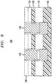
- Figure 4 shows a fourth step in the process wherein a Si 3 N 4 layer 140 is formed on the upper surface of the device 100.
- the layer 140 preferably has a thickness in a range from 50 angstroms to 500 angstroms.
- the Si 3 N 4 film layer 140 substantially prevents electrical shorting which may occur between the base substrate layer 110 and the upper silicon layer 120.
- Figure 5 shows a fifth step in the process wherein a masking film 150 is deposited on specified portions of the upper surface of the device 100.
- the masking film 150 is preferably formed of a photoresist material, however, other suitable masking films may also be used.
- the masking film 150 covers all portions of the upper surface of the device 100 except trench 300.
- the masking layer 150 is deposited, it is exposed and the portion of the layer 140 deposited in the trench 300 is etched away to expose the conductive layer 135 at the bottom of the trench.
- Figure 7 shows a sixth step in the process wherein a third insulator layer 160 is laid down in the trench 300 on the conductive layer 135.
- the third insulator layer is preferably formed of silicon dioxide, but may be formed of other suitable insulators.
- the third insulator layer may be formed by growing silicon dioxide on the conductive layer 135 (if the conductive layer is formed of silicon), or by deposition (which would require an additional masking step, as is well known in the art).
- the third insulator layer 160 preferably has an area in a range from 1 square micron to 500 square microns.
- Figure 8 shows a seventh step in the process wherein portions of the Si 3 N 4 film layer 140 are removed.
- a second masking layer 165, and an anisotropic etch process are used to remove the second oxide resistant film layer 140 from the bottom of the trench 310, and from the upper surface of the device 100, respectively.
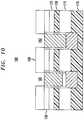
- Figure 9 shows an eighth step in the process wherein a second conductive layer 170 is used to fill both of the trenches 300, 310.
- the second conductive layer 170 may be formed of silicon, and is preferably formed of polysilicon.
- the second conductive layer 170 is deposited in the trenches 300, 310, and then the upper surface of the device 100 is planarized (using well known techniques such as Chemical Mechanical Polishing (CMP)) to form the device as shown in Figure 9 .
- CMP Chemical Mechanical Polishing
- Figure 10 shows a ninth step in the process wherein a dielectric layer 180 is deposited on the device and portions overlying the trenches 300, 310 are etched away.
- the dielectric layer 180 may be formed of materials such as silicon nitride (Si 3 N 4 ), silicon dioxide (SiO 2 ), and silicon oxynitride (SiON), or any other suitable dielectric material.
- the dielectric layer 180 may be deposited by processes well known in the art, such as chemical vapor deposition (CVD).
- CVD chemical vapor deposition
- vias 181, 182 are etched in the dielectric material to expose the trenches 300, 310.
- the vias 181, 182 may be formed by conventional patterning and etching techniques which are well known in the art.
- Figure 11 shows an tenth (and final) step in the process wherein conductive contacts 190 are formed on the upper surface of the device 100.
- Conductive contacts 190 are signal contact landings which allow the coupling of electrical signals to the capacitor device 100.
- the conductive contacts may be formed of any suitable conductor, however, metals are preferred.
- the upper surface of the device 100 may be planarized (by CMP or otherwise) at this point, so that the conductive contacts 190 are flush with the dielectric layer 180, and so that additional levels may be formed on the upper surface of the device.
- the above-described process may be utilized to form a capacitor device 100 as shown in Figure 11 .
- the conductive layers 135 and 170 formed in trench 300 form a first electrode of the capacitor, and the portions of the base substrate layer 110 which are adjacent to the trench 300 form a second electrode of the capacitor.
- Contact to the first electrode may be made via metal land 300 which overlies trench 300, and contact to the second electrode may be made via metal land 300 which overlies trench 310.
- an aspect of the present invention is a trench capacitor formed on a SOI substrate and having an electrode (second) formed by regions of the base substrate layer 110 which are adjacent to the trench and which are disposed beneath the insulating layer 115 of the SOI substrate.
- a further aspect of the present invention is the contact structure (trench 310) formed in close proximity to the trench capacitor, and which extends through the insulating layer 115 of the SOI substrate. Accordingly, the conductive layers 135 and 170 formed in the trench 300 form a first electrode of the semiconductor capacitor, and the portions of the base substrate layer 110 which bound the trench 300 form a second electrode of the semiconductor capacitor which may be contacted via the contact structure formed in trench 310.
- Yet another advantage of the present invention is that the uppermost surface (i.e., the surface with conductive contacts 190) of the device 100 is planar, thereby allowing the formation of additional levels on the upper surface of the device without the need for intervening layering steps.
Description
- The present invention relates to semiconductor devices and in particular to trench capacitors.
- Semiconductor devices typically utilize capacitors to perform various functions, such as electric charge storage, for example. A standard capacitor includes two electrodes or "plates" separated from each other by a dielectric insulating material. The electrodes are typically formed of electrically conductive or semiconductive materials. The ability of a capacitor to store an electric charge depends on the capacitor area. Since many capacitors are formed above the surface of a semiconductor substrate, as the area of the capacitor increases (to increase the charge-holding capacity), the space left available on the semiconductor substrate for other devices is decreased. As a result, in order to minimize the surface area occupied by capacitors, trench capacitors have become highly favored in the semiconductor manufacturing industry.
- Trench capacitors extend down from the surface of the semiconductor substrate. Thus, instead of being formed on the surface of the semiconductor substrate, the capacitor is formed in a trench which is dug in the semiconductor substrate. Accordingly, the capacitor area (and implicitly the charge-holding capacity of the capacitor) may be increased by increasing the depth and width of the trench. As will be understood, the formation of the capacitor beneath the surface of the semiconductor substrate frees up space on the surface of the semiconductor substrate for additional devices.
- A recent trend in the semiconductor industry has been towards the use of silicon-on-insulator (SOI) semiconductor substrates. A standard SOI substrate includes a doped base substrate layer (typically formed of silicon), an insulator layer, and an upper doped silicon layer. SOI substrates are favored because active devices formed within an upper silicon layer are insulated from the base substrate. Therefore, device leakage through the substrate is minimized, and problems associated electrical coupling to the substrate are reduced or eliminated.
-
US Patent 5 770 875 discloses a trench capacitor arrangement on silicon-on-insulator substrate in which capacitors are formed by trenches which are coated with a dielectric layer and filled with a conductive material. A second capacitor plate is formed by a doped region of the based substrate layer and is contacted by a trench without dielectric coating.EP 0 848 418 A2 discloses a method for forming a trench capacitor in a silicon-on-insulator substrate, in which one electrode is formed by a doped region adjacent to a trench in the substrate base layer and the second electrode is formed of a conductive filling in the trench. - The use of SOI substrates, however, presents a problem since trench openings formed in the substrate (used to form, for example, trench capacitors) must extend through the insulating layer in order for the trench capacitor to have sufficient area, thereby exposing the upper silicon layer to the base substrate layer. The problem results because the silicon base substrate layer can become electrically shorted to the upper silicon layer.
- Therefore, there is currently a need for a trench capacitor which is at least partially formed in the silicon base substrate layer of an SOI substrate, and which provides electrical isolation between the silicon base substrate layer and the upper silicon layers of the SOI substrate.
- The present invention is a semiconductor device including a silicon-on-insulator substrate including a base substrate, an insulator layer, and a silicon layer, and a trench capacitor including at least one trench formed in the silicon-on-insulator substrate and extending through the base substrate, the insulator layer and the silicon layer, in accordance with the independent claim 1.
- The above and other advantages and features of the present invention will be better understood from the following detailed description of the preferred embodiments of the invention which is provided in connection with the accompanying drawings.
-
-
Figures 1-11 show a process sequence used to form a capacitor and contact structure according to an exemplary embodiment of the present invention: -
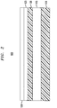
Figure 1 is a side cross-sectional view showing a silicon-on-insulator (SOI) substrate. -
Figure 2 is a side cross-sectional view showing a silicon-on-insulator substrate with a second insulator layer and an oxide resistant film formed on the SOI substrate. -
Figure 3 is a side cross-sectional view showing a silicon-on-insulator substrate showing the formation of a pair of trenches, which are filled with a conductive layer. -
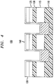
Figure 4 is a side cross-sectional view showing the formation of a Si3N4 film layer. -
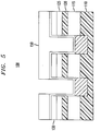
Figure 5 is a side cross-sectional view showing the formation of a masking layer. -
Figure 6 is a side cross-sectional view showing the etching away of the Si3N4 layer in one of the trenches. -
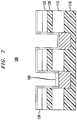
Figure 7 is a side cross-sectional view showing the formation of a third insulator layer in one of the trenches. -
Figure 8 is a side cross-sectional view showing the masking and etching away of portions of the Si3N4 layer. -
Figure 9 is a side cross-sectional view showing the formation of a second conductive layer. -
Figure 10 is a side cross-sectional view showing the formation of a dielectric layer. -
Figure 11 is a side cross-sectional view showing the formation of conductive contacts. - Referring to
Figures 1-11 , there is shown a process for forming asemiconductor capacitor device 100 according to an exemplary embodiment of the present invention. -
Figure 1 shows a silicon-on-insulator (SOI) substrate formed of a semiconductorbase substrate layer 110, aninsulator layer 115, and asilicon layer 120. The semiconductorbase substrate layer 110 may be formed of a silicon (Si) wafer, as is well known in the semiconductor manufacturing industry, however, other materials may also be used for the semiconductor base substrate layer without departing from the scope of the invention.Insulator layer 115 may be formed of silicon dioxide (SiO2), however, other insulators may also be utilized.Silicon layer 120 may be a crystal silicon layer, an amorphous silicon layer, or may be a polycrystalline silicon layer (commonly referred to as polysilicon). A thickness of theinsulator layer 115 may be in a range 200 angstroms to 6000 angstroms, and a thickness of thesilicon layer 120 may be in a range 500 angstroms to 4000 angstroms. However, it should be noted that the above ranges are only suggested dimensions, and that the thicknesses of theinsulator layer 115 andsilicon layer 120 may be in any suitable range. -
Figure 2 shows a second step in the process wherein asecond insulator layer 125 and an oxideresistant film layer 130 are successively laid down on thesilicon layer 120. As above, the second insulator layer may be SiO2 or any other suitable insulator. The oxideresistant film layer 130 may be formed of silicon nitride (Si3N4), titanium nitride (TiN), tungsten nitride (WN), tantalum nitride (TaN), or any other suitable oxide resistant material. A thickness of thesecond insulator layer 125 may be in a range from 100 angstroms to 500 angstroms. A thickness of the oxideresistant film layer 130 may be in a range from 50 angstroms to 5000 angstroms, and preferably in a range from 300 to 600 angstroms. Thesecond insulator layer 125 and the oxideresistant film layer 130 are laid down on thesilicon layer 120 by processes well known in the semiconductor manufacturing industry. -
Figure 3 shows a third step in the process wherein trenches 300, 310 are formed and filled with aconductive material 135, such as silicon (preferably doped polysilicon). Thetrenches trenches Figure 3 , thetrenches base substrate layer 110. The width of thetrench 300 preferably varies from. 1 microns to 2-3 microns, and the depth of the trench preferably varies from .5 microns to 6 microns. An "aspect ratio" of thetrench 300 is defined as the ratio of the depth to the width, and is preferably less than or equal to 6.Trench 310, may have the same or similar dimensions to that oftrench 300, but such a geometry is not required. For simplicity,trenches trench 300 forms a trench capacitor andtrench 310 forms a contact structure for contacting thebase substrate layer 110 of the SOI substrate. Theconductive layer 135 may be formed by growing epitaxial silicon on thebase substrate layer 120, or by deposition processes well known in the art (e.g., Chemical Vapor Deposition (CVD)). -
Figure 4 shows a fourth step in the process wherein a Si3N4 layer 140 is formed on the upper surface of thedevice 100. Thelayer 140 preferably has a thickness in a range from 50 angstroms to 500 angstroms. The Si3N4 film layer 140 substantially prevents electrical shorting which may occur between thebase substrate layer 110 and theupper silicon layer 120. -
Figure 5 shows a fifth step in the process wherein amasking film 150 is deposited on specified portions of the upper surface of thedevice 100. Themasking film 150 is preferably formed of a photoresist material, however, other suitable masking films may also be used. In the exemplary embodiment, the maskingfilm 150 covers all portions of the upper surface of thedevice 100 excepttrench 300. - As shown in
Figure 6 , after themasking layer 150 is deposited, it is exposed and the portion of thelayer 140 deposited in thetrench 300 is etched away to expose theconductive layer 135 at the bottom of the trench. -
Figure 7 shows a sixth step in the process wherein athird insulator layer 160 is laid down in thetrench 300 on theconductive layer 135. The third insulator layer is preferably formed of silicon dioxide, but may be formed of other suitable insulators. The third insulator layer may be formed by growing silicon dioxide on the conductive layer 135 (if the conductive layer is formed of silicon), or by deposition (which would require an additional masking step, as is well known in the art). Thethird insulator layer 160 preferably has an area in a range from 1 square micron to 500 square microns. -
Figure 8 shows a seventh step in the process wherein portions of the Si3N4 film layer 140 are removed. Asecond masking layer 165, and an anisotropic etch process are used to remove the second oxideresistant film layer 140 from the bottom of thetrench 310, and from the upper surface of thedevice 100, respectively. -
Figure 9 shows an eighth step in the process wherein a secondconductive layer 170 is used to fill both of thetrenches conductive layer 170 may be formed of silicon, and is preferably formed of polysilicon. First, the secondconductive layer 170 is deposited in thetrenches device 100 is planarized (using well known techniques such as Chemical Mechanical Polishing (CMP)) to form the device as shown inFigure 9 . -
Figure 10 shows a ninth step in the process wherein adielectric layer 180 is deposited on the device and portions overlying thetrenches dielectric layer 180 may be formed of materials such as silicon nitride (Si3N4), silicon dioxide (SiO2), and silicon oxynitride (SiON), or any other suitable dielectric material. Thedielectric layer 180 may be deposited by processes well known in the art, such as chemical vapor deposition (CVD). After thedielectric layer 180 is formed on the entire surface of thedevice 100, vias 181, 182 are etched in the dielectric material to expose thetrenches vias -
Figure 11 shows an tenth (and final) step in the process whereinconductive contacts 190 are formed on the upper surface of thedevice 100.Conductive contacts 190 are signal contact landings which allow the coupling of electrical signals to thecapacitor device 100. The conductive contacts may be formed of any suitable conductor, however, metals are preferred. The upper surface of thedevice 100 may be planarized (by CMP or otherwise) at this point, so that theconductive contacts 190 are flush with thedielectric layer 180, and so that additional levels may be formed on the upper surface of the device. - Thus, the above-described process may be utilized to form a
capacitor device 100 as shown inFigure 11 . Theconductive layers trench 300 form a first electrode of the capacitor, and the portions of thebase substrate layer 110 which are adjacent to thetrench 300 form a second electrode of the capacitor. Contact to the first electrode may be made viametal land 300 which overliestrench 300, and contact to the second electrode may be made viametal land 300 which overliestrench 310. - It is to be emphasized, that an aspect of the present invention is a trench capacitor formed on a SOI substrate and having an electrode (second) formed by regions of the
base substrate layer 110 which are adjacent to the trench and which are disposed beneath the insulatinglayer 115 of the SOI substrate. A further aspect of the present invention is the contact structure (trench 310) formed in close proximity to the trench capacitor, and which extends through the insulatinglayer 115 of the SOI substrate. Accordingly, theconductive layers trench 300 form a first electrode of the semiconductor capacitor, and the portions of thebase substrate layer 110 which bound thetrench 300 form a second electrode of the semiconductor capacitor which may be contacted via the contact structure formed intrench 310. - Yet another advantage of the present invention is that the uppermost surface (i.e., the surface with conductive contacts 190) of the
device 100 is planar, thereby allowing the formation of additional levels on the upper surface of the device without the need for intervening layering steps.
Claims (8)
- A semiconductor device (100) comprising:a silicon-on-insulator substrate including a base substrate layer (110), a first insulator layer (115) located on the base substrate layer (110), and a silicon layer (120) located on the insulator layer (115), a second insulator layer (125) disposed on the silicon layer (120) of the silicon-on-insulator substrate, and an oxide resistant film layer (130) disposed on the second insulator layer (125), anda trench capacitor (300) extending through the oxide resistant film layer (130), the second insulator layer (125), the silicon layer (120) and the first insulator layer (11S) and into the base substrate layer (110), anda capacitor contact trench (310) located in the silicon-on-insulator substrate and extending through the silicon layer (120) and the first insulator layer (115) into the base substrate (110), the capacitor contact trench (310) providing electrical contact to the trench capacitor (300) through the base substrate layer (110),characterized in thata first conductive layer (135) is formed at a bottom of the trench capacitor (300) and the capacitor contact trench (310), respectively, said first conductive layer (135) being formed on the base substrate layer (110) and extending up to the first insulator layer (115),a Si3N4 layer (140) is formed on the surface of the trenches of the trench capacitor (300) and the capacitor contact trench (310), respectively, the Si3N4 layer (140) extending from an upper surface of the oxide resistant film layer (130) and terminating at the first conductive layer (135) in the trench capacitor (300) and the capacitor contact trench (310), for preventing electrical shorting which may occur between the base substrate layer (110) and the silicon layer (120), anda third insulator layer (160) is located in the trench capacitor (300) on the first conductive layer (135), anda second conductive layer (170) is located in the trench capacitor (300) over the third insulator layer (160) and in the capacitor contact trench (310) over the first conductive layer (135), anda dielectric layer (180) is deposited on the oxide resistant film layer (130) and on the Si3N4 layers (140), andconductive contacts (190) are formed on the upper surface of the device (100) to contact the second conductive layer (170).
- The semiconductor device (100) of claim 1, wherein the third insulator layer (160) comprises silicon dioxide.
- The semiconductor device (100) of claim 1, wherein the first conductive layer (135) comprises a layer of silicon.
- The semiconductor device (100) of claim 1, wherein the first and second conductive layers (135, 170) comprise layers of silicon.
- The semiconductor device (100) of claim 1, wherein the first conductive layer (135) in the trench capacitor (300) forms a first plate of the trench capacitor (300).
- The semiconductor device (100) of claim 5, wherein portions of said base substrate layer (110) which are adjacent to the trench capacitor (300) form a second electrode of the trench capacitor (300).
- The semiconductor device (100) of claim 1, wherein the first and second conductive layers (135, 170) comprise silicon.
- The semiconductor device (100) of claim 1, wherein a surface of the device (100) is substantially planar.
Applications Claiming Priority (2)
| Application Number | Priority Date | Filing Date | Title |
|---|---|---|---|
| US09/611,907 US6538283B1 (en) | 2000-07-07 | 2000-07-07 | Silicon-on-insulator (SOI) semiconductor structure with additional trench including a conductive layer |
| US611907 | 2000-07-07 |
Publications (2)
| Publication Number | Publication Date |
|---|---|
| EP1170786A1 EP1170786A1 (en) | 2002-01-09 |
| EP1170786B1 true EP1170786B1 (en) | 2019-06-19 |
Family
ID=24450876
Family Applications (1)
| Application Number | Title | Priority Date | Filing Date |
|---|---|---|---|
| EP01114983.8A Expired - Lifetime EP1170786B1 (en) | 2000-07-07 | 2001-06-20 | Silicon-on-insulator (SOI) semiconductor structure |
Country Status (5)
| Country | Link |
|---|---|
| US (1) | US6538283B1 (en) |
| EP (1) | EP1170786B1 (en) |
| JP (1) | JP4931291B2 (en) |
| KR (1) | KR100753788B1 (en) |
| TW (1) | TWI282168B (en) |
Families Citing this family (5)
| Publication number | Priority date | Publication date | Assignee | Title |
|---|---|---|---|---|
| US6825545B2 (en) * | 2003-04-03 | 2004-11-30 | International Business Machines Corporation | On chip decap trench capacitor (DTC) for ultra high performance silicon on insulator (SOI) systems microprocessors |
| US7569450B2 (en) * | 2006-06-09 | 2009-08-04 | International Business Machines Corporation | Semiconductor capacitors in hot (hybrid orientation technology) substrates |
| US7880267B2 (en) * | 2006-08-28 | 2011-02-01 | Micron Technology, Inc. | Buried decoupling capacitors, devices and systems including same, and methods of fabrication |
| US8399957B2 (en) * | 2011-04-08 | 2013-03-19 | International Business Machines Corporation | Dual-depth self-aligned isolation structure for a back gate electrode |
| CN103066007B (en) * | 2012-12-14 | 2018-01-02 | 上海集成电路研发中心有限公司 | A kind of preparation method of full isolation structure |
Family Cites Families (18)
| Publication number | Priority date | Publication date | Assignee | Title |
|---|---|---|---|---|
| US4534076A (en) | 1982-05-05 | 1985-08-13 | Barge Fred H | Reclining radiographic wall table |
| JPS62136869A (en) * | 1985-12-11 | 1987-06-19 | Sony Corp | Semiconductor memory device |
| JPS63242241A (en) | 1987-03-31 | 1988-10-07 | 株式会社東芝 | Trouble detector of moving quantity detection means |
| US5155758A (en) | 1990-04-19 | 1992-10-13 | Thomas Vogl | Portable device for facilitating the performance of radiographic procedures |
| US5349956A (en) | 1991-12-04 | 1994-09-27 | Apogee Medical Products, Inc. | Apparatus and method for use in medical imaging |
| US5386447A (en) | 1992-09-23 | 1995-01-31 | Fischer Imaging Corporation | Mammographic screening and biopsy apparatus |
| JP3260449B2 (en) | 1992-10-22 | 2002-02-25 | 株式会社東芝 | X-ray diagnostic equipment |
| US5305365A (en) | 1992-11-24 | 1994-04-19 | Bennett X-Ray Technologies | Mammography system with rearwardly tilting mammograph |
| JP3535542B2 (en) * | 1993-09-22 | 2004-06-07 | エルジイ・セミコン・カンパニイ・リミテッド | Semiconductor memory device and method of manufacturing the same |
| JPH08222710A (en) | 1995-02-17 | 1996-08-30 | Mitsubishi Electric Corp | Semiconductor device |
| SE505513C2 (en) | 1995-11-14 | 1997-09-08 | Elekta Ab | Device for repositioning a patient |
| US5585285A (en) | 1995-12-06 | 1996-12-17 | Micron Technology, Inc. | Method of forming dynamic random access memory circuitry using SOI and isolation trenches |
| US5770875A (en) * | 1996-09-16 | 1998-06-23 | International Business Machines Corporation | Large value capacitor for SOI |
| US5770484A (en) * | 1996-12-13 | 1998-06-23 | International Business Machines Corporation | Method of making silicon on insulator buried plate trench capacitor |
| KR19980084637A (en) * | 1997-05-23 | 1998-12-05 | 김영환 | Method for forming charge storage electrode of semiconductor device |
| DE19736884A1 (en) | 1997-08-25 | 1999-03-18 | Siemens Ag | Expanded diagnostic magnetic resonance device with operation functionality |
| US5976945A (en) | 1997-11-20 | 1999-11-02 | Vanguard International Semiconductor Corporation | Method for fabricating a DRAM cell structure on an SOI wafer incorporating a two dimensional trench capacitor |
| KR20050075638A (en) * | 2004-01-17 | 2005-07-21 | 삼성전자주식회사 | Method of fabricating trench capacitor using soi type wafer |
-
2000
- 2000-07-07 US US09/611,907 patent/US6538283B1/en not_active Expired - Lifetime
-
2001
- 2001-06-20 EP EP01114983.8A patent/EP1170786B1/en not_active Expired - Lifetime
- 2001-06-28 JP JP2001196104A patent/JP4931291B2/en not_active Expired - Fee Related
- 2001-07-02 TW TW090116133A patent/TWI282168B/en not_active IP Right Cessation
- 2001-07-06 KR KR1020010040533A patent/KR100753788B1/en not_active IP Right Cessation
Non-Patent Citations (1)
| Title |
|---|
| None * |
Also Published As
| Publication number | Publication date |
|---|---|
| EP1170786A1 (en) | 2002-01-09 |
| US6538283B1 (en) | 2003-03-25 |
| TWI282168B (en) | 2007-06-01 |
| KR100753788B1 (en) | 2007-08-31 |
| JP2002064146A (en) | 2002-02-28 |
| JP4931291B2 (en) | 2012-05-16 |
| KR20020005494A (en) | 2002-01-17 |
Similar Documents
| Publication | Publication Date | Title |
|---|---|---|
| US6897107B2 (en) | Method for forming TTO nitride liner for improved collar protection and TTO reliability | |
| EP0682372B1 (en) | DRAM device with upper and lower capacitor and production method | |
| US6649959B2 (en) | Method for increasing a very-large-scale-integrated (VLSI) capacitor size on bulk silicon and silicon-on-insulator (SOI) wafers and structure formed thereby | |
| EP0771022A2 (en) | Precision metal-metal capacitor for analog circuit | |
| US7678696B2 (en) | Method of making through wafer vias | |
| US20020071237A1 (en) | Capacitor having sidewall spacer protecting the dielectric layer and method of fabricating the same | |
| US6261895B1 (en) | Polysilicon capacitor having large capacitance and low resistance and process for forming the capacitor | |
| US6847077B2 (en) | Capacitor for a semiconductor device and method for fabrication therefor | |
| KR20030022951A (en) | Method of manufacturing the electric wiring and method of manufacturing the semiconductor device the same | |
| US5574621A (en) | Integrated circuit capacitor having a conductive trench | |
| US6664581B2 (en) | Damascene capacitor having a recessed plate | |
| US20020155654A1 (en) | Vertical gate top engineering for improved GC and CB process windows | |
| KR20010006086A (en) | Capacitors in integrated circuits | |
| US6552381B2 (en) | Trench capacitors in SOI substrates | |
| KR100335778B1 (en) | Semiconductor device and a method of manufacturing thereof | |
| EP1073124A2 (en) | Method for making integrated circuit capacitor including anchored plug | |
| KR100294755B1 (en) | Semiconductor device and its manufacturing method | |
| KR20040074355A (en) | Wiring formed by employing a damascene process, method for forming the wiring, semiconductor device including the same, and method for manufacturing the semiconductor device | |
| EP1170786B1 (en) | Silicon-on-insulator (SOI) semiconductor structure | |
| US6706588B1 (en) | Method of fabricating an integrated circuit having embedded vertical capacitor | |
| KR20010029962A (en) | Method for making integrated circuit capacitor including anchored plugs | |
| US5953618A (en) | Method of forming a capacitor for a semiconductor device | |
| EP1073114A2 (en) | Integrated circuit capacitor including anchored metal plug | |
| KR20010015483A (en) | Method of making integrated circuit capacitor including tapered plug | |
| EP1020928A1 (en) | Thin film capacitor including an anchored metal plug |
Legal Events
| Date | Code | Title | Description |
|---|---|---|---|
| PUAI | Public reference made under article 153(3) epc to a published international application that has entered the european phase |
Free format text: ORIGINAL CODE: 0009012 |
|
| AK | Designated contracting states |
Kind code of ref document: A1 Designated state(s): GB Kind code of ref document: A1 Designated state(s): AT BE CH CY DE DK ES FI FR GB GR IE IT LI LU MC NL PT SE TR |
|
| AX | Request for extension of the european patent |
Free format text: AL;LT;LV;MK;RO;SI |
|
| 17P | Request for examination filed |
Effective date: 20020513 |
|
| AKX | Designation fees paid |
Free format text: GB |
|
| REG | Reference to a national code |
Ref country code: DE Ref legal event code: 8566 |
|
| 17Q | First examination report despatched |
Effective date: 20080801 |
|
| RAP1 | Party data changed (applicant data changed or rights of an application transferred) |
Owner name: AVAGO TECHNOLOGIES GENERAL IP (SINGAPORE) PTE. LTD |
|
| RIC1 | Information provided on ipc code assigned before grant |
Ipc: H01L 27/12 20060101AFI20181121BHEP |
|
| GRAP | Despatch of communication of intention to grant a patent |
Free format text: ORIGINAL CODE: EPIDOSNIGR1 |
|
| INTG | Intention to grant announced |
Effective date: 20190207 |
|
| RIN1 | Information on inventor provided before grant (corrected) |
Inventor name: KELLY, MICHAEL J. Inventor name: CHITTIPEDDI, SAILESH |
|
| GRAS | Grant fee paid |
Free format text: ORIGINAL CODE: EPIDOSNIGR3 |
|
| GRAA | (expected) grant |
Free format text: ORIGINAL CODE: 0009210 |
|
| AK | Designated contracting states |
Kind code of ref document: B1 Designated state(s): GB |
|
| REG | Reference to a national code |
Ref country code: GB Ref legal event code: FG4D |
|
| PGFP | Annual fee paid to national office [announced via postgrant information from national office to epo] |
Ref country code: GB Payment date: 20190722 Year of fee payment: 19 |
|
| PLBE | No opposition filed within time limit |
Free format text: ORIGINAL CODE: 0009261 |
|
| STAA | Information on the status of an ep patent application or granted ep patent |
Free format text: STATUS: NO OPPOSITION FILED WITHIN TIME LIMIT |
|
| 26N | No opposition filed |
Effective date: 20200603 |
|
| GBPC | Gb: european patent ceased through non-payment of renewal fee |
Effective date: 20200620 |
|
| PG25 | Lapsed in a contracting state [announced via postgrant information from national office to epo] |
Ref country code: GB Free format text: LAPSE BECAUSE OF NON-PAYMENT OF DUE FEES Effective date: 20200620 |