EP1164639B1 - Alignment marks for manufacturing semiconductor device - Google Patents
Alignment marks for manufacturing semiconductor device Download PDFInfo
- Publication number
- EP1164639B1 EP1164639B1 EP01114247A EP01114247A EP1164639B1 EP 1164639 B1 EP1164639 B1 EP 1164639B1 EP 01114247 A EP01114247 A EP 01114247A EP 01114247 A EP01114247 A EP 01114247A EP 1164639 B1 EP1164639 B1 EP 1164639B1
- Authority
- EP
- European Patent Office
- Prior art keywords
- alignment
- layer
- layers
- alignment mark
- area
- Prior art date
- Legal status (The legal status is an assumption and is not a legal conclusion. Google has not performed a legal analysis and makes no representation as to the accuracy of the status listed.)
- Expired - Lifetime
Links
Images








Classifications
-
- H—ELECTRICITY
- H10—SEMICONDUCTOR DEVICES; ELECTRIC SOLID-STATE DEVICES NOT OTHERWISE PROVIDED FOR
- H10W—GENERIC PACKAGES, INTERCONNECTIONS, CONNECTORS OR OTHER CONSTRUCTIONAL DETAILS OF DEVICES COVERED BY CLASS H10
- H10W46/00—Marks applied to devices, e.g. for alignment or identification
-
- G—PHYSICS
- G03—PHOTOGRAPHY; CINEMATOGRAPHY; ANALOGOUS TECHNIQUES USING WAVES OTHER THAN OPTICAL WAVES; ELECTROGRAPHY; HOLOGRAPHY
- G03F—PHOTOMECHANICAL PRODUCTION OF TEXTURED OR PATTERNED SURFACES, e.g. FOR PRINTING, FOR PROCESSING OF SEMICONDUCTOR DEVICES; MATERIALS THEREFOR; ORIGINALS THEREFOR; APPARATUS SPECIALLY ADAPTED THEREFOR
- G03F9/00—Registration or positioning of originals, masks, frames, photographic sheets or textured or patterned surfaces, e.g. automatically
- G03F9/70—Registration or positioning of originals, masks, frames, photographic sheets or textured or patterned surfaces, e.g. automatically for microlithography
- G03F9/7073—Alignment marks and their environment
- G03F9/7084—Position of mark on substrate, i.e. position in (x, y, z) of mark, e.g. buried or resist covered mark, mark on rearside, at the substrate edge, in the circuit area, latent image mark, marks in plural levels
-
- H—ELECTRICITY
- H10—SEMICONDUCTOR DEVICES; ELECTRIC SOLID-STATE DEVICES NOT OTHERWISE PROVIDED FOR
- H10W—GENERIC PACKAGES, INTERCONNECTIONS, CONNECTORS OR OTHER CONSTRUCTIONAL DETAILS OF DEVICES COVERED BY CLASS H10
- H10W46/00—Marks applied to devices, e.g. for alignment or identification
- H10W46/301—Marks applied to devices, e.g. for alignment or identification for alignment
-
- H—ELECTRICITY
- H10—SEMICONDUCTOR DEVICES; ELECTRIC SOLID-STATE DEVICES NOT OTHERWISE PROVIDED FOR
- H10W—GENERIC PACKAGES, INTERCONNECTIONS, CONNECTORS OR OTHER CONSTRUCTIONAL DETAILS OF DEVICES COVERED BY CLASS H10
- H10W46/00—Marks applied to devices, e.g. for alignment or identification
- H10W46/501—Marks applied to devices, e.g. for alignment or identification for use before dicing
- H10W46/503—Located in scribe lines
-
- H—ELECTRICITY
- H10—SEMICONDUCTOR DEVICES; ELECTRIC SOLID-STATE DEVICES NOT OTHERWISE PROVIDED FOR
- H10W—GENERIC PACKAGES, INTERCONNECTIONS, CONNECTORS OR OTHER CONSTRUCTIONAL DETAILS OF DEVICES COVERED BY CLASS H10
- H10W20/00—Interconnections in chips, wafers or substrates
- H10W20/40—Interconnections external to wafers or substrates, e.g. back-end-of-line [BEOL] metallisations or vias connecting to gate electrodes
-
- H—ELECTRICITY
- H10—SEMICONDUCTOR DEVICES; ELECTRIC SOLID-STATE DEVICES NOT OTHERWISE PROVIDED FOR
- H10W—GENERIC PACKAGES, INTERCONNECTIONS, CONNECTORS OR OTHER CONSTRUCTIONAL DETAILS OF DEVICES COVERED BY CLASS H10
- H10W46/00—Marks applied to devices, e.g. for alignment or identification
- H10W46/501—Marks applied to devices, e.g. for alignment or identification for use before dicing
Definitions
- the present invention relates to a semiconductor device and a method of manufacturing the same, and more particularly, relates to a semiconductor device that can reduce an area occupied by an alignment mark such as a scribe line formed in an alignment area and a method of manufacturing the same.
- a semiconductor device having a multilayer wiring structure is formed by means of stacking a plurality of insulation layers or wiring layers using a photolithography, but an alignment mark is used in positioning the patterns transferred by the photolithography with respect to each layer.
- the alignment marks have various shapes according to the exposing system, but, generally, are formed by means of arranging marks having angle of several ⁇ m in several to several tens of matrix shapes.
- the positioning of a semiconductor substrate is performed by means of exposing the alignment mark to a laser beam and detecting the reflected right thereof. Then, after a layer is formed, wiring and through holes are formed by means of performing process such as etching to the layer using a resist pattern to which a mask pattern is transferred.
- FIGs. 1A through 1G are cross sectional views schematically and sequentially showing a forming method of an alignment mark in the manufacturing processes of the semiconductor device according to the first prior art, and illustrate cross sections of an alignment area such as a scribe line. Also, this prior art shows only an alignment area, and does not show a circuit pattern area where transistor and the like are formed.
- predetermined transistor, etc. are formed (not shown) in a circuit pattern area of a semiconductor substrate such as Si (not shown).
- a first insulation layer 1 comprised of a silicon oxide film, etc. is formed, and then, after a metal layer of Al, etc. is deposited, a resist layer is formed, and then, an alignment is performed by using a mark (not shown) previously formed on the semiconductor substrate which becomes a base as a reference, after that, the resist layer is exposed.
- process such as a dry etching is carried out by using a resist pattern formed by the exposure as a mask, so that a first wiring layer is formed in the circuit pattern area, and at the same time, an alignment mark 2a comprised of the same metal layer as the first wiring layer is formed in the alignment area such as the scribe line.
- the alignment mark explained in the prior art is comprised of about several tens of rows with three columns of marks arranged at predetermined intervals, and the cross section of a line direction will be explained.
- a resist layer is formed, and an exposure is carried out by means of using the alignment mark 2a as a reference. And, a dry etching process is performed by using a resist pattern formed by the exposure as a mask, so that first through holes are formed in the circuit pattern area, and at the same time, an alignment mark 3a in which the first through holes are arranged is formed in the alignment area.
- the first through holes are formed on the first wiring layer in the circuit pattern area which is not shown, but because the first wiring layer is not formed under the second insulation layer 3 in the alignment area shown in Fig. 1A , the thickness of the second insulation layer 3 is thicker than that of the circuit pattern area.
- the first through holes in the alignment area do not penetrate the second insulation layer 3, and have a shape that the etching is stopped in the middle portion of the second insulation layer 3.
- a metal layer such as Al is deposited on the second insulation layer 3
- a resist pattern (not shown) is formed by performing an alignment by using the alignment mark 3a depositing the metal layer as a reference.
- a dry etching process is performed by means of using the resist pattern as a mask, so that a second wiring layer 4 is formed in the circuit pattern area.
- an alignment mark 4a is formed in the alignment area.
- a predetermined resist layer (not shown) is formed, and then, an exposure is performed by using the alignment mark 4a formed of the second wiring layer 4 as a reference, so that a resist pattern (not shown) having a predetermined opening is formed.
- a dry etching is performed by means of using the resist pattern as a mask, so that second through holes penetrating the third insulation layer 5 are formed in the circuit pattern area, and at the same time, an alignment mark 5a in which the second through holes are arranged is formed in the alignment area.
- a metal layer such as Al is deposited on the third insulation layer 5
- a predetermined resist layer is formed, and then, an alignment is performed by using the alignment mark 5a depositing the metal layer as a reference, so that a resist pattern (not shown) is formed.
- a dry etching process is performed by using the resist pattern as a mask, so that a third wiring layer 6 is formed in the circuit pattern area, and at the same time, as shown in Fig. 1F , an alignment mark 6a is formed in the alignment area.
- a semiconductor device as shown in Fig. 1G in which a plurality of wiring layers (seven layers in this prior art) are stacked is manufactured by repeating the same processes sequentially.
- the alignment marks having the same number as the sum of the deposited wiring layers and insulation layers are formed in a new place in the alignment area.
- total fourteen alignment marks including the insulation layers are formed.
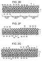
- Figs. 2A through 2G and Fig. 3 are improvement of the first prior art, are cross sectional views sequentially showing the second prior art to reduce an area occupied by an alignment mark, and illustrate only an alignment area similarly to the above-mentioned first prior art.
- a semiconductor substrate such as Si
- a first insulation layer 1 comprised of a silicon oxide layer, etc. and a metal layer of Al, etc. are deposited.
- a predetermined resist layer (not shown) is formed, and an exposure is performed by means of using a mark (not shown) previously formed on a predetermined position of the semiconductor substrate as a reference, so that a resist pattern is formed.
- a dry etching is performed by means of using the resist pattern as a mask, so that a first wiring layer is formed in a circuit pattern area, and at the same time, an alignment mark 2a in which the metal layer is arranged in a matrix shape is formed in a first area of an alignment area.
- a resist predetermined layer (not shown) is formed, and then, an exposure is performed by means of using the first alignment mark 2a as a reference. And, a dry etching is performed by using a resist pattern (not shown) formed by the exposure as a mask, so that first through holes penetrating the second insulation layer 3 are formed in the circuit pattern area, and at the same time, an alignment mark 3a in which the first through holes are arranged in a matrix shape is formed in a second area of the alignment area.
- the reason why the alignment mark 3a does not penetrate the second insulation layer 3 and etching is stopped in the middle portion of the second insulation layer 3 is the same as that of the above-mentioned first prior art.
- a predetermined resist layer (not shown) is formed, and then, a resist pattern (not shown) is formed by performing an alignment by means of using the alignment mark 3a comprised of the first through holes formed in the previous process as a reference. And, a dry etching process is performed by using the resist pattern as a mask, however, in the second prior art, an alignment mark 4a comprised of the second wiring layer 4 is formed in a third area of the scribe line, and at the same time, a light-shielding layer 4d is formed in the upper part of the alignment mark 2a in the first area.
- a predetermined resist layer (not shown) is formed, and then, an exposure is performed by using the alignment mark 4a as a reference, so that a resist pattern (not shown) having an opening is formed on the light-shielding layer 4d.
- a dry etching is performed by means of using the resist pattern as a mask, so that second through holes penetrating the third insulation layer 5 are formed in the circuit pattern area, and an alignment mark 5a reaching the light-shielding layer 4d is formed in the first area of the alignment area.
- a metal layer such as A1 is deposited on the third insulation layer 5
- a predetermined resist layer (not shown) is formed, and then, an alignment performed by using the alignment mark 5a comprised of the second through holes formed in the previous process as a reference, so that a resist pattern (not shown) is formed.
- a dry etching process is performed by using the resist pattern as a mask, so that an alignment mark 6a comprised of the third wiring layer 6 is formed in a fourth area of the alignment area, and at the same time, a light-shielding layer 6d is formed in the upper part of the alignment mark 4a in the third area.
- a predetermined resist layer (not shown) is formed, and then, an exposure is performed by using the alignment mark 6a in the fourth area as a reference, so that a resist pattern (not shown) having an opening is formed on the light-shielding layer 6d.
- a dry etching is performed by means of using the resist pattern as a mask, so that an alignment mark 7a comprised of third through holes reaching the light-shielding layer 6d is formed in the third area where the light-shielding layer 6d is formed.
- a semiconductor device shown in Fig. 3 can be manufactured by repeating the above-mentioned processes of Figs. 2A through 2G .
- US-A-5 545 593 discloses a method of aligning layers in an integrated circuit device including associating an alignment target with each layer.
- Each alignment target has multiple edges created through a boxed frame configuration and during semiconductor device fabrication, each alignment target is formed into an alignment structure on the semiconductor wafer.
- one alignment target of one layer falls within the alignment target of a correspondingly aligned layer within the alignment structure.
- An object of the present invention is to provide a semiconductor device that can reduce an area occupied by the alignment mark of a scribe line without separately providing a metal layer having a large size such as a light-shielding layer and a method of manufacturing the same.
- a method of manufacturing a semiconductor device wherein a multilayer wiring structure in which wiring layers and insulation layers are alternately stacked are formed, and an alignment of each layer is performed by using an alignment mark provided in a predetermined alignment area.
- Said method comprises the steps of: performing the alignment of each wiring layer with respect to previously formed layers by using an alignment mark formed of a plurality of through holes provided in the insulation layer just under said wiring layer, when forming said wiring layer; and performing the alignment of each insulation layer with respect to previously formed layers by using an alignment mark provided in the lowermost wiring layer, when forming the through holes in each of said insulation layers, wherein said alignment marks formed in each of said insulation layers are sequentially formed in two or three areas within said predetermined alignment area so that each of said two or three areas comprises marks provided in at least two different insulation layers, and said alignment marks in each area are arranged so as to be overlapped with each other as seen in a normal direction to the substrate.
- underlays having a larger shape than that of said through holes, at the same step of forming each wiring layer, at a position which is aligned to each through hole of the alignment mark which is going to be formed in the insulation layer just above said wiring layer and wherein the underlays within each wiring layer are formed to be separated from each other.
- an etching of said wiring layer may be performed so as to form a convex portion extended outwardly from an inner wall of said through hole on an upper edge of each through hole of said alignment mark formed in said insulation layer just under said wiring layer.
- a semiconductor device having a multilayer wiring structure in which wiring layers and insulation layers are alternately stacked, and an alignment of each layer is performed by using an alignment mark provided in a predetermined alignment areas of a scribe-line.
- Said semiconductor device comprises: alignment marks having through holes provided in said insulation layers, to be used in the alignment of said wiring layers with respect to said insulation layers; and an alignment mark provided in the lowermost wiring layer, to be used in the alignment of all of said insulation layers, wherein said alignment marks formed in each of said insulation layers are sequentially formed in two or three areas within said predetermined alignment area, and said alignment marks in each area are arranged so as to be overlapped with each other as seen in a normal direction to the substrate.
- underlays are formed, at the same step of forming each wiring layer just under said insulation layer, in the lower part of each through hole of said alignment mark formed in each of said insulation layers.
- a shape of each of said underlays is larger than that of said through holes as seen in a normal direction to the substrate.
- a convex portion may be provided formed of the wiring layer just above said insulation layer and extended outwardly from an upper edge of said through hole of said alignment mark formed in each of said insulation layers.
- the present invention since through holes are formed in all the insulation layers deposited above the first wiring layer and in a polyimide layer which is an uppermost layer to be used as a protection layer of a semiconductor device by using an alignment mark which is formed with the first wiring layer, and alignment marks formed of the through holes are overlapped with each other, and the alignment marks are not formed in a new area when forming the through holes in the insulation layer, the area occupied by the alignment marks can be reduced, thereby, the chip size can be effectively utilized.
- a saucer which becomes a underlay is formed in the lower area of the through holes, and an alignment mark is formed by means of penetrating the through holes up to the saucer, so that an uniformity of an alignment mark shape in a wafer surface can be improved, thereby, the effect that the pattern of the wiring layer on the through holes can be precisely formed is exhibited.
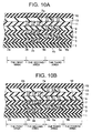
- an alignment is performed by using an alignment mark (2a in Fig. 10A and Fig. 10B ) provided in a first wiring layer of the lowermost layer, and alignment marks (3a, 5a, 7a in Fig. 10A and Fig. 10B ) provided in an insulation layer are formed by being alternately overlapped in two areas such as a scribe line, so that an area occupied by the alignment marks can be reduced.
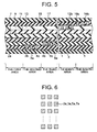
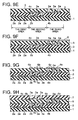
- Figs. 4A through 4H and Fig. 5 are cross sectional views sequentially showing a method of manufacturing a semiconductor device according to the example, and illustrate cross sections of an alignment area such as a scribe line where an alignment marks are formed.
- Fig. 6 is a plan view schematically showing the arrangement of the alignment mark used in the present invention
- Figs. 7 and 8 are the measured data showing the intensity distribution of the laser beam for alignment reflected from the alignment mark.
- a device isolating-insulation layer and a gate electrode are formed on a semiconductor substrate (not shown) such as Si, and a predetermined transistor is formed (not shown).
- a semiconductor substrate such as Si
- a predetermined transistor is formed (not shown).
- a first insulating layer 1 comprised of a silicon oxide layer is deposited in the thickness of about 1.3 ⁇ m
- a through hole is formed in a predetermined area of a circuit pattern area (not shown).
- a base metal of Ti/TiN, etc. is deposited in the thickness of about 70 nm by sputtering method
- a metal layer of Al, etc. is formed in the thickness of about 400 nm.
- a resist layer is formed, and an exposure is performed by means of using a mark (not shown) previously formed in the semiconductor substrate as a reference.
- a dry etching such as plasma etching is performed by means of using a resist pattern formed by the exposure as a mask, so that a first wiring layer (not shown) is formed in the circuit pattern area.
- a dry etching such as plasma etching is performed by means of using a resist pattern formed by the exposure as a mask, so that a first wiring layer (not shown) is formed in the circuit pattern area.
- an alignment mark 2a in which the metal layers are arranged in a matrix shape is formed in a first area of an alignment area, and at the same time, a saucer 2b that becomes an underlay of through holes to be formed in the next process is formed in a second area.
- an alignment mark uses a mark having shape that three columns of marks are arranged in several tens of rows at predetermined intervals.
- a flattening is performed by Chemical Mechanical Polishing (CMP) process or etchback process, and a silicon oxide layer, etc. are deposited again, so that a second insulation layer 3 of about 1.3 ⁇ m in thickness is formed.
- CMP Chemical Mechanical Polishing
- a predetermined resist layer is formed, and then, an exposure is performed by means of using the alignment mark 2a comprised of the first wiring layer as a reference.
- a dry etching is performed by using a resist pattern formed by the exposure as a mask, so that first through holes are formed in the circuit pattern area, and at the same time, an alignment mark 3a in which the first through holes are arranged in a matrix shape is formed on the saucer 2b in a second area of the alignment area.
- the thickness of the second insulation layer 3 is the same as those of the circuit pattern area and the alignment area, so that the second alignment mark 3a is formed by penetrating the second insulation layer.
- the thickness of the insulation layer forming the through hole there is a case that a step of the through holes becomes too smaller to perform an alignment due to a saucer 2b, but in this case, it is unnecessary to form the saucer 2b.
- a resist layer is formed, and then, an exposure is performed by using the alignment mark 3a depositing the metal layers in the first through holes as a reference.
- an uniformity of the alignment mark shape in a wafer surface can be improved, so that an measurement error of the alignment mark can be reduced.
- a dry etching is performed by means of using a resist pattern (not shown) formed by the exposure as a mask, so that a second wiring layer 4 is formed in the circuit pattern area.
- a new alignment mark is not formed in the alignment area, but a saucer 4b which becomes an underlay for the through holes of a third insulation 5 to be formed thereon is formed in a third area. Further, a lid 4c pushed out of the through holes may be formed on the alignment mark 3a. The lid 4c can prevent sidewalls comprised of the second wiring layer 4 deposited on the inner walls of the alignment mark 3a from being peeled off.
- a third insulation layer 5 comprised of a silicon oxide layer, etc. is deposited in the thickness of about 1.3 ⁇ m on the second wiring layer 4, a predetermined resist layer (not shown) is formed, and then, an exposure is performed.
- the alignment mark 2a formed of the first wiring layer in Fig. 4A is used.
- the alignment of the third insulation layer 5 has been performed by using an alignment mark formed of the second wiring layer 4 just under the third insulation layer 5, however in the present example, since a stacked layer of the third insulation layer 5 and the second insulation layer 3 can sufficiently transmit a laser beam such as He-Ne and a halogen light for the alignment and a metal layer reflecting an alignment light is not formed in the upper part of the first alignment mark 2a, the alignment is performed by using the alignment mark 2a as a reference.
- the exposure is performed by using the alignment mark 2a as a reference, and a resist pattern having an opening is formed on the saucer 4b formed of the second wiring layer 4, and then, a dry etching is performed by using the resist pattern as a mask, so that the second through holes penetrating the third insulation layer 5 are formed in the circuit pattern area, and the alignment mark 5a in which the second through holes are arranged is formed on the saucer 4b in the third area of the alignment area.
- a third wiring layer 6 is formed in the circuit pattern area by using the alignment mark 5a comprised of the second through holes formed in the previous process as a reference, and at the same time, as shown in Fig. 4G , a saucer 6b which becomes a underlay of the alignment mark comprised of the through holes to be formed thereon is formed in a fourth area of the alignment area.
- a fourth insulation layer 7 comprised of a silicon oxide layer, etc. is deposited on the third wiring layer 6, as the process in Fig.
- an alignment light such as a laser beam of He-Ne and a halogen light can sufficiently transmit the stacked insulation layers.
- an experimental alignment mark was formed on a sixth wiring layer 12, and the alignment for forming a through hole in a seventh insulation layer 13 was performed by using the alignment mark 2a formed of the first wiring layer and the above-mentioned experimental alignment mark, respectively, and the intensity of the signal from the both alignments was compared. The results thereof are shown in Fig. 7 and Fig. 8 .
- Fig. 7 and Fig. 8 show an intensity distribution of the alignment lights reflected from the alignment marks
- Fig. 7 shows data of the experimental alignment mark formed of the sixth wiring layer 12 shown in the seventh area
- Fig. 8 shows data of the alignment mark 2a formed of the first wiring layer.
- a horizontal axis indicates a distance on a scribe line
- a vertical axis indicates an intensity of the reflected light.
- the alignment light is a waveform after passing through six layers of the second to the seventh insulation layers, the waveform of the reflected light is not different from that of Fig. 7 transmitting only the seventh insulation layer, and it can be known that the alignment can be performed by using only the alignment mark 2a formed of the first wiring layer.
- the waveform of reflected right is dependent on the conditions such as materials and thickness of the insulation layers to which the light is transmitted, but the inventor of the present invention have confirmed that the first alignment mark 2a can be used in manufacturing a semiconductor device having the structure depositing eight layers of Ti/TiN and Al as a wiring layer, depositing silicon oxide layers of about 1.3 ⁇ m in thickness as an insulation layer between the wiring layers, and depositing a protection layer comprised of polyimide on the uppermost surface.
- the through holes can be formed in all the insulation layers deposited in the upper layer of the first wiring layer by using the alignment mark 2a formed in processing the first wiring layer, it is unnecessary to form new alignment marks on each wiring layer, and the number of alignment marks can be reduced comparing to the prior art. Consequently, the alignment area can be reduced, and other accessory or a check pattern for confirming an operation, etc. can be arranged. Further, since it is unnecessary to form a metal layer such as a light-shielding layer having large size unlike the prior art, in case where an alignment area is formed in a scribe line, there is no possibility that short occurs due to scattering of metal pieces during dicing process.
- the above-mentioned effect is achieved in case of providing three or more wiring layers, and the more layers are provided, the more effects are exhibited, but according to the experiment conducted by the inventor of the present invention, it has been confirmed that a semiconductor device in which eight wiring layers are stacked can be manufactured by using the above-mentioned method.
- the present example described the case using Ti/TiN and Al as a material of the wiring layer, and a silicon oxide layer as a material of the insulation layer
- the present invention is not limited to the above-mentioned embodiment, and other conductive materials such as tungsten can be used as a wiring layer, and a silicon nitride layer, a stacked layer consisted of a silicon oxide layer and a silicon nitride layer, SOG and other insulating materials can be used as an insulation layer.
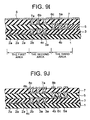
- Figs. 9A through 9J , Fig. 10A and Fig. 10B are cross sectional views sequentially showing a method of manufacturing the semiconductor device according to the first embodiment, and illustrate a configuration of an alignment area such as a scribe line where alignment marks are formed.
- the present embodiment is different from the example in view that the through holes in the insulation layers are formed by being alternately stacked so as to more reduce the area occupied by the alignment mark, and other conditions are the same as those of the first embodiment.
- a device isolating-insulation layer and a gate electrode are formed on a semiconductor substrate (not shown) such as Si, and then, a first insulation layer 1 comprised of a silicon oxide layer, etc. is deposited in the thickness of about 1.3 ⁇ m thereon.
- a first wiring layer (not shown) is formed in a circuit pattern area, and at the same time, a first alignment mark 2a d is formed in a first area of an alignment, and a saucer 2b which becomes an underlay of through holes formed in the next process is formed in a second area of an alignment area.
- a second insulation layer 3 comprised of a silicon oxide layer, etc. is deposited on the first wiring layer, and a flattening is performed by CMP process or etchback process so as to be about 1.3 ⁇ m in thickness, and then, by using the first alignment mark 2a as a reference, first through holes are formed in the circuit area, and at the same time, an alignment mark 3a in which the first through holes are arranged in a matrix shape is formed on the saucer 2b in the second area of the alignment area.
- a metal layer such as Al is deposited on the second insulation layer 3
- an exposure is performed by means of using the alignment mark 3a as a reference, so that a second wiring layer 4 is formed in the circuit pattern area, and at the same time, a saucer 4b which becomes an underlay of through holes in the third insulation layer 5 to be formed thereon is formed in a third area, and a lid 4c pushed out of the first through holes is formed in the second area.
- a third insulation layer 5 is deposited on the first wiring layer, in the same manner as the above-mentioned example, an exposure is performed by means of using the alignment mark 2a formed of the first wiring layer as a reference, so that second through holes penetrating the third insulation layer 5 are formed by in the circuit pattern area, and at the same time, an alignment mark 5a in which the second through holes are arranged is formed on the saucer 4b in the third area.
- a metal layer such as Al is deposited on the third insulation layer 5.
- a third wiring layer 6 is formed by using the alignment mark 5a comprised of the second through holes formed in the previous process as a reference.
- a saucer 6b which becomes an underlay of alignment mark comprised of the through holes to be formed thereon is formed by being overlapped with the second area of a scribe line and the like in which the saucer formed of the first wiring layer is arranged.
- the saucer 6b since the saucer 6b is formed in the lower part of the third through holes, the saucer 6b becomes an etch stopper although a dry etching for forming the third through holes is performed excessively, and thus, the third through holes are never connected to the third through holes of the lower layer. Further, when performing the alignment for forming a fourth wiring layer 8, since the wiring layer metal covers all the substrate, the alignment mark 3a comprised of the first through holes of the lower layer or the second wiring layer 4 formed in the first through holes does not become an obstacle to the alignment.
- a laser beam for alignment sufficiently transmit the insulation layers
- an alignment for forming the through holes in the insulation layer of the upper layer can be performed by using the alignment mark 2a comprised of the first wiring layer as a reference.
- a preliminary alignment mark 18 is formed on any wiring layer (the fourth wiring layer 9 in Fig. 10B ), so that it may be used instead of the alignment mark 2a.
- the through holes are formed in all the insulation layers deposited above the first wiring layer by using the alignment mark 2a formed when processing the first wiring layer and the through holes are formed alternately at a position overlapped with the through holes in the lower layer, the number of alignment marks and an area occupied by the alignment mark can be more reduced than that of the above-mentioned example.
- a chip size can be effectively utilized, and other accessory or a check pattern for confirming an operation can be arranged.
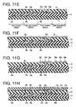
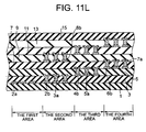
- Fig. 11A through Fig. 11L are cross sectional views sequentially showing a method of second manufacturing a semiconductor device according to the second embodiment, and illustrate a configuration of a scribe line area where alignment marks are formed.
- the present embodiment is different from the above-mentioned first embodiment in view that through holes of insulation layers are formed by being sequentially stacked in three areas, and other conditions are the same as those of the second embodiment.
- a first insulation layer 1, a first wiring layer, an alignment mark 2a and a saucer 2b, an alignment mark 3a comprised of a second insulation layer 3 and first through holes, a second wiring layer 4 and a saucer 4b, and an alignment mark 5a comprised of a third insulation layer 5 and second through holes are formed on a semiconductor substrate (not shown) such as Si.
- a third wiring layer 6 is formed by using the alignment mark 5a comprised of the second through holes as a reference, but in the present embodiment, unlike the first embodiment, as shown in Fig. 11G , a saucer 6b which becomes an underlay of an alignment mark comprised of through holes to be formed thereon is formed in a fourth area of an alignment area. Further, as shown in Fig. 11F , after metal layers such as Ti/TiN and Al are deposited in the thickness of about 70 nm and 400 nm, respectively, a third wiring layer 6 is formed by using the alignment mark 5a comprised of the second through holes as a reference, but in the present embodiment, unlike the first embodiment, as shown in Fig. 11G , a saucer 6b which becomes an underlay of an alignment mark comprised of through holes to be formed thereon is formed in a fourth area of an alignment area. Further, as shown in Fig.
- a metal layer of Al, etc. is deposited on the fourth insulation layer 7
- an exposure is performed by using the alignment mark 7a as a reference, so that a saucer 8b which becomes an underlay of through holes of the fourth insulation layer 9 to be formed thereon and a lid 8c pushed out of the third through holes are formed in the second area of the alignment area.
- a semiconductor device in which a plurality of wiring layers are stacked in multilayer can be manufactured by repeating the same processes.
- the through holes are formed by being overlapped in three areas sequentially, and it is because in case where according to a thickness of each insulation layer, unevenness in the lid for preventing sidewalls formed in the through holes from being peeled off is reflected on the saucer in the upper layer thereof, so that the shape of through holes may be disordered, thereby, in this case, an affect caused by the unevenness is relieved by forming more insulation layers inserted between the upper and lower through holes. Accordingly, an area where the through holes are formed is three in the present embodiment, but the number of the areas can be properly increased according to the manufacturing conditions.
- the alignment mark 2a formed of the first wiring layer is used as a reference when forming the through holes in the upper insulation layer.
- a preliminary alignment mark may be provided on any wiring layer.
- the through holes are formed in all the insulation layers deposited on the first wiring layer by using the alignment mark 2a formed of the first wiring layer, and the through holes are formed in three areas at a position sequentially overlapped with the through holes in the lower layer, thereby, comparing to the prior art that a new alignment mark is formed in each wiring layer, the number of the alignment marks and the area occupied by the alignment mark can be more reduced.
Landscapes
- Physics & Mathematics (AREA)
- General Physics & Mathematics (AREA)
- Internal Circuitry In Semiconductor Integrated Circuit Devices (AREA)
- Exposure And Positioning Against Photoresist Photosensitive Materials (AREA)
- Exposure Of Semiconductors, Excluding Electron Or Ion Beam Exposure (AREA)
Description
- The present invention relates to a semiconductor device and a method of manufacturing the same, and more particularly, relates to a semiconductor device that can reduce an area occupied by an alignment mark such as a scribe line formed in an alignment area and a method of manufacturing the same.
- A semiconductor device having a multilayer wiring structure is formed by means of stacking a plurality of insulation layers or wiring layers using a photolithography, but an alignment mark is used in positioning the patterns transferred by the photolithography with respect to each layer. The alignment marks have various shapes according to the exposing system, but, generally, are formed by means of arranging marks having angle of several µm in several to several tens of matrix shapes. The positioning of a semiconductor substrate is performed by means of exposing the alignment mark to a laser beam and detecting the reflected right thereof. Then, after a layer is formed, wiring and through holes are formed by means of performing process such as etching to the layer using a resist pattern to which a mask pattern is transferred.
- In this case, a method of manufacturing a semiconductor device using the conventional alignment mark will be discussed with reference to
Figs. 1A through 1G (first prior art).Figs. 1A through 1G are cross sectional views schematically and sequentially showing a forming method of an alignment mark in the manufacturing processes of the semiconductor device according to the first prior art, and illustrate cross sections of an alignment area such as a scribe line. Also, this prior art shows only an alignment area, and does not show a circuit pattern area where transistor and the like are formed. - First, predetermined transistor, etc. are formed (not shown) in a circuit pattern area of a semiconductor substrate such as Si (not shown). Next, as shown in
Fig. 1A , afirst insulation layer 1 comprised of a silicon oxide film, etc. is formed, and then, after a metal layer of Al, etc. is deposited, a resist layer is formed, and then, an alignment is performed by using a mark (not shown) previously formed on the semiconductor substrate which becomes a base as a reference, after that, the resist layer is exposed. And, process such as a dry etching is carried out by using a resist pattern formed by the exposure as a mask, so that a first wiring layer is formed in the circuit pattern area, and at the same time, analignment mark 2a comprised of the same metal layer as the first wiring layer is formed in the alignment area such as the scribe line. Further, the alignment mark explained in the prior art is comprised of about several tens of rows with three columns of marks arranged at predetermined intervals, and the cross section of a line direction will be explained. - Next, after a
second insulation layer 3 is deposited on the first wiring layer, a resist layer is formed, and an exposure is carried out by means of using thealignment mark 2a as a reference. And, a dry etching process is performed by using a resist pattern formed by the exposure as a mask, so that first through holes are formed in the circuit pattern area, and at the same time, analignment mark 3a in which the first through holes are arranged is formed in the alignment area. - In addition, the first through holes are formed on the first wiring layer in the circuit pattern area which is not shown, but because the first wiring layer is not formed under the
second insulation layer 3 in the alignment area shown inFig. 1A , the thickness of thesecond insulation layer 3 is thicker than that of the circuit pattern area. In this case, since the condition of the dry etching to form the through holes are set according to the thickness of the insulation layer in the circuit pattern area, the first through holes in the alignment area do not penetrate thesecond insulation layer 3, and have a shape that the etching is stopped in the middle portion of thesecond insulation layer 3. - Next, as shown
Fig. 1B , after a metal layer such as Al is deposited on thesecond insulation layer 3, a predetermined resist layer (not shown) is formed, and then, a resist pattern (not shown) is formed by performing an alignment by using thealignment mark 3a depositing the metal layer as a reference. A dry etching process is performed by means of using the resist pattern as a mask, so that asecond wiring layer 4 is formed in the circuit pattern area. In addition, as shown inFig. 1C , analignment mark 4a is formed in the alignment area. - Next, as shown in
Fig. 1D , after athird insulation layer 5 is deposited on thesecond wiring layer 4, a predetermined resist layer (not shown) is formed, and then, an exposure is performed by using thealignment mark 4a formed of thesecond wiring layer 4 as a reference, so that a resist pattern (not shown) having a predetermined opening is formed. After that, a dry etching is performed by means of using the resist pattern as a mask, so that second through holes penetrating thethird insulation layer 5 are formed in the circuit pattern area, and at the same time, analignment mark 5a in which the second through holes are arranged is formed in the alignment area. - Next, as shown in
Fig. 1E , after a metal layer such as Al is deposited on thethird insulation layer 5, a predetermined resist layer is formed, and then, an alignment is performed by using thealignment mark 5a depositing the metal layer as a reference, so that a resist pattern (not shown) is formed. A dry etching process is performed by using the resist pattern as a mask, so that athird wiring layer 6 is formed in the circuit pattern area, and at the same time, as shown inFig. 1F , analignment mark 6a is formed in the alignment area. After that, a semiconductor device as shown inFig. 1G in which a plurality of wiring layers (seven layers in this prior art) are stacked is manufactured by repeating the same processes sequentially. - As such, conventionally, when forming the patterns of each
wiring layer alignment marks insulation layers wiring layers alignment marks insulation layer alignment marks wiring layers 2, 4 just under the insulation layers, and thealignment marks - That is, in case of alternately stacking wiring layers and insulation layers, since new alignment marks are formed according to the formation of the wiring layers and the through holes in the insulation layers, the alignment marks having the same number as the sum of the deposited wiring layers and insulation layers are formed in a new place in the alignment area. In detail, in case where seven wiring layers are formed as shown in the present prior art, total fourteen alignment marks including the insulation layers are formed.
- However, in the recent semiconductor devices having a multilayer wiring structure, because the number of alignment marks are increased by making in a multilayer form, and at the same time, more accurate alignment is demanded by minuteness, the arranged number of the marks constituting alignment mark are increased, and an area occupied by one alignment mark becomes great. On the other hand, since a shape of the alignment mark are determined by the used exposing system, the shape thereof cannot be changed freely, and the area occupied by the alignment mark in the alignment area such as a scribe line as a whole semiconductor device becomes great, and thus, there is a problem that other accessory or check pattern for confirming the operation of the semiconductor device cannot be inserted into the scribe line.
- As a method of solving the problem, the official Japanese Patent application published under
JP-A-9-232207 Figs. 2A through 2G andFig. 3 .Figs. 2A through 2G andFig. 3 are improvement of the first prior art, are cross sectional views sequentially showing the second prior art to reduce an area occupied by an alignment mark, and illustrate only an alignment area similarly to the above-mentioned first prior art. - First, in the same manner as the above-mentioned first prior art, after predetermined transistor, etc. are formed on a semiconductor substrate (not shown) such as Si, as shown in
Fig. 2A , afirst insulation layer 1 comprised of a silicon oxide layer, etc. and a metal layer of Al, etc. are deposited. Next, a predetermined resist layer (not shown) is formed, and an exposure is performed by means of using a mark (not shown) previously formed on a predetermined position of the semiconductor substrate as a reference, so that a resist pattern is formed. And, a dry etching is performed by means of using the resist pattern as a mask, so that a first wiring layer is formed in a circuit pattern area, and at the same time, analignment mark 2a in which the metal layer is arranged in a matrix shape is formed in a first area of an alignment area. - Next, after a
second insulation layer 3 is deposited on the first wiring layer, a resist predetermined layer (not shown) is formed, and then, an exposure is performed by means of using thefirst alignment mark 2a as a reference. And, a dry etching is performed by using a resist pattern (not shown) formed by the exposure as a mask, so that first through holes penetrating thesecond insulation layer 3 are formed in the circuit pattern area, and at the same time, analignment mark 3a in which the first through holes are arranged in a matrix shape is formed in a second area of the alignment area. In addition, the reason why thealignment mark 3a does not penetrate thesecond insulation layer 3 and etching is stopped in the middle portion of thesecond insulation layer 3 is the same as that of the above-mentioned first prior art. - Next, as shown in
Figs. 2B and 2C , after a metal layer is deposited on thesecond insulation layer 3, a predetermined resist layer (not shown) is formed, and then, a resist pattern (not shown) is formed by performing an alignment by means of using thealignment mark 3a comprised of the first through holes formed in the previous process as a reference. And, a dry etching process is performed by using the resist pattern as a mask, however, in the second prior art, analignment mark 4a comprised of thesecond wiring layer 4 is formed in a third area of the scribe line, and at the same time, a light-shielding layer 4d is formed in the upper part of thealignment mark 2a in the first area. - Next, as shown in
Fig. 2D , after athird insulation layer 5 is deposited on thesecond wiring layer 4, a predetermined resist layer (not shown) is formed, and then, an exposure is performed by using thealignment mark 4a as a reference, so that a resist pattern (not shown) having an opening is formed on the light-shielding layer 4d. After that, a dry etching is performed by means of using the resist pattern as a mask, so that second through holes penetrating thethird insulation layer 5 are formed in the circuit pattern area, and analignment mark 5a reaching the light-shielding layer 4d is formed in the first area of the alignment area. - Next, as shown in
Fig. 2E and Fig. 2F , after a metal layer such as A1 is deposited on thethird insulation layer 5, a predetermined resist layer (not shown) is formed, and then, an alignment performed by using thealignment mark 5a comprised of the second through holes formed in the previous process as a reference, so that a resist pattern (not shown) is formed. And, a dry etching process is performed by using the resist pattern as a mask, so that analignment mark 6a comprised of thethird wiring layer 6 is formed in a fourth area of the alignment area, and at the same time, a light-shielding layer 6d is formed in the upper part of thealignment mark 4a in the third area. - Next, as shown in
Fig. 2G , after afourth insulation layer 7 is deposited on thethird wiring layer 6, a predetermined resist layer (not shown) is formed, and then, an exposure is performed by using thealignment mark 6a in the fourth area as a reference, so that a resist pattern (not shown) having an opening is formed on the light-shielding layer 6d. After that, a dry etching is performed by means of using the resist pattern as a mask, so that analignment mark 7a comprised of third through holes reaching the light-shielding layer 6d is formed in the third area where the light-shielding layer 6d is formed. After that, a semiconductor device shown inFig. 3 can be manufactured by repeating the above-mentioned processes ofFigs. 2A through 2G . - In the method described in the above-mentioned second prior art, since
other alignment marks layers - The use of a single set of alignment marks on a wafer which may be preserved throughout a multilevel integrated circuit fabrication is disclosed in C. Lapadula, B.J. Lin, "DICHROIC ALIGNMENT MARKS", IBM Technical Disclosure Bulletin, Vol. 21, No. 5, October 1978. This is achieved by coating dichroic alignment marks on photoexposure masks, so that the alignment marks are transparent to the radiation used for alignment, but opaque to the exposing radiation.
-
US-A-5 545 593 discloses a method of aligning layers in an integrated circuit device including associating an alignment target with each layer. Each alignment target has multiple edges created through a boxed frame configuration and during semiconductor device fabrication, each alignment target is formed into an alignment structure on the semiconductor wafer. For correspondingly aligned layers, one alignment target of one layer falls within the alignment target of a correspondingly aligned layer within the alignment structure. - An object of the present invention is to provide a semiconductor device that can reduce an area occupied by the alignment mark of a scribe line without separately providing a metal layer having a large size such as a light-shielding layer and a method of manufacturing the same.
- According to one aspect of the present invention, there is provided a method of manufacturing a semiconductor device, wherein a multilayer wiring structure in which wiring layers and insulation layers are alternately stacked are formed, and an alignment of each layer is performed by using an alignment mark provided in a predetermined alignment area. Said method comprises the steps of: performing the alignment of each wiring layer with respect to previously formed layers by using an alignment mark formed of a plurality of through holes provided in the insulation layer just under said wiring layer, when forming said wiring layer; and performing the alignment of each insulation layer with respect to previously formed layers by using an alignment mark provided in the lowermost wiring layer, when forming the through holes in each of said insulation layers, wherein said alignment marks formed in each of said insulation layers are sequentially formed in two or three areas within said predetermined alignment area so that each of said two or three areas comprises marks provided in at least two different insulation layers, and said alignment marks in each area are arranged so as to be overlapped with each other as seen in a normal direction to the substrate.
- According to the present invention, it is required to form underlays having a larger shape than that of said through holes, at the same step of forming each wiring layer, at a position which is aligned to each through hole of the alignment mark which is going to be formed in the insulation layer just above said wiring layer and wherein the underlays within each wiring layer are formed to be separated from each other.
- Also, when forming said wiring layer, an etching of said wiring layer may be performed so as to form a convex portion extended outwardly from an inner wall of said through hole on an upper edge of each through hole of said alignment mark formed in said insulation layer just under said wiring layer.
- According to another aspect of the present invention, there is provided a semiconductor device having a multilayer wiring structure in which wiring layers and insulation layers are alternately stacked, and an alignment of each layer is performed by using an alignment mark provided in a predetermined alignment areas of a scribe-line. Said semiconductor device comprises: alignment marks having through holes provided in said insulation layers, to be used in the alignment of said wiring layers with respect to said insulation layers; and an alignment mark provided in the lowermost wiring layer, to be used in the alignment of all of said insulation layers, wherein said alignment marks formed in each of said insulation layers are sequentially formed in two or three areas within said predetermined alignment area, and said alignment marks in each area are arranged so as to be overlapped with each other as seen in a normal direction to the substrate.
- According to the present invention, it is required that underlays are formed, at the same step of forming each wiring layer just under said insulation layer, in the lower part of each through hole of said alignment mark formed in each of said insulation layers. A shape of each of said underlays is larger than that of said through holes as seen in a normal direction to the substrate.
- Also, a convex portion may be provided formed of the wiring layer just above said insulation layer and extended outwardly from an upper edge of said through hole of said alignment mark formed in each of said insulation layers.
- According to the present invention, since through holes are formed in all the insulation layers deposited above the first wiring layer and in a polyimide layer which is an uppermost layer to be used as a protection layer of a semiconductor device by using an alignment mark which is formed with the first wiring layer, and alignment marks formed of the through holes are overlapped with each other, and the alignment marks are not formed in a new area when forming the through holes in the insulation layer, the area occupied by the alignment marks can be reduced, thereby, the chip size can be effectively utilized.
- Further, according to the present invention, a saucer which becomes a underlay is formed in the lower area of the through holes, and an alignment mark is formed by means of penetrating the through holes up to the saucer, so that an uniformity of an alignment mark shape in a wafer surface can be improved, thereby, the effect that the pattern of the wiring layer on the through holes can be precisely formed is exhibited.
- In addition, according to the present invention, since it is unnecessary to provide a light-shielding layer for preventing the light reflected from the alignment mark of the lower layer, occurrence of metal film pieces causing short in providing the semiconductor device can be prevented.
- The above objects, other objects, features and advantages of the present invention will be better understood from the following description taken in conjunction with the accompanying drawings, in which:
-
Figs. 1A through 1G are cross sectional views sequentially showing a method of manufacturing a semiconductor device using an alignment mark according to the first prior art; -
Figs. 2A through 2G are cross sectional views sequentially showing a method of manufacturing a semiconductor device using an alignment mark of the second prior art; -
Fig. 3 is a cross sectional view showing the next process ofFig. 2G ; -
Figs. 4A through 4H are cross sectional views sequentially showing a method of manufacturing a semiconductor device according to an example not forming part of the present invention; -
Fig. 5 is a cross sectional view showing the next process ofFig. 4H ; -
Fig. 6 is a plan view schematically showing the arrangement of the alignment mark used in the present invention; -
Fig. 7 is a measured data showing an intensity distribution of the laser beam reflected from the alignment mark which is experimentally formed with a sixth wiring layer provided in the seventh area, wherein a vertical axis indicates an intensity of the reflected laser beam and a horizontal axis indicates a length along the scribe line; -
Fig. 8 is a measured data showing an intensity distribution of the laser beam reflected from the alignment mark which is experimentally formed with a first wiring layer, wherein a vertical axis indicates an intensity of the reflected laser beam and a horizontal axis indicates a length along the scribe line; -
Figs. 9A through 9J are cross sectional views sequentially showing a method of manufacturing a semiconductor device according to the first embodiment of the present invention; -
Fig. 10A is a cross sectional view sequentially showing the next process ofFig. 9J , andFig. 10B is a cross sectional view showing a modified embodiment of the first embodiment of the present invention; and -
Figs. 11A through 11L are cross sectional views sequentially showing a method of manufacturing a semiconductor device according to the second embodiment of the present invention. - Hereinafter, a semiconductor device and a method of manufacturing the same according to the embodiments of the present invention will be described in detail with reference to the accompanying drawings.
- In a method of manufacturing a semiconductor device having a multilayer wiring structure according to the present invention, as one preferred embodiment, when forming through holes in the first to eighth insulation layers, an alignment is performed by using an alignment mark (2a in
Fig. 10A and Fig. 10B ) provided in a first wiring layer of the lowermost layer, and alignment marks (3a, 5a, 7a inFig. 10A and Fig. 10B ) provided in an insulation layer are formed by being alternately overlapped in two areas such as a scribe line, so that an area occupied by the alignment marks can be reduced. - In order to explain the above-mentioned preferred embodiment of the present invention in detail, the embodiments of the present invention will be described with reference to the accompanying drawings.
- First, a method of manufacturing a semiconductor device using an alignment mark according to an example not forming part of the present invention will be described with reference to
Figs. 4A through 4H ,Fig. 5 ,Fig. 6 ,Fig. 7 and Fig. 8 .Figs. 4A through 4H andFig. 5 are cross sectional views sequentially showing a method of manufacturing a semiconductor device according to the example, and illustrate cross sections of an alignment area such as a scribe line where an alignment marks are formed. Also,Fig. 6 is a plan view schematically showing the arrangement of the alignment mark used in the present invention, andFigs. 7 and 8 are the measured data showing the intensity distribution of the laser beam for alignment reflected from the alignment mark. - First, a device isolating-insulation layer and a gate electrode are formed on a semiconductor substrate (not shown) such as Si, and a predetermined transistor is formed (not shown). After that, as shown in
Fig. 4A , after a first insulatinglayer 1 comprised of a silicon oxide layer is deposited in the thickness of about 1.3 µm, a through hole is formed in a predetermined area of a circuit pattern area (not shown). Next, after a base metal of Ti/TiN, etc. is deposited in the thickness of about 70 nm by sputtering method, a metal layer of Al, etc. is formed in the thickness of about 400 nm. Subsequently, a resist layer is formed, and an exposure is performed by means of using a mark (not shown) previously formed in the semiconductor substrate as a reference. - And, a dry etching such as plasma etching is performed by means of using a resist pattern formed by the exposure as a mask, so that a first wiring layer (not shown) is formed in the circuit pattern area. At this time, an
alignment mark 2a in which the metal layers are arranged in a matrix shape is formed in a first area of an alignment area, and at the same time, asaucer 2b that becomes an underlay of through holes to be formed in the next process is formed in a second area. - In this case, because a shape of the
saucer 2b is slightly larger than that of the through hole and saucers are formed to be separated from each other, the metal layer having a large size can be prevented from remaining in the scribe line as the prior art. Further, as explained later, by means of providing asaucer 2b, the thickness of the insulation layer formed in the upper layer thereof can be equal to those of the circuit pattern area and the alignment area, and an uniformity of the alignment mark shapes in a wafer surface can be improved. In addition, as shown inFig. 6 , an alignment mark uses a mark having shape that three columns of marks are arranged in several tens of rows at predetermined intervals. - Next, as shown in
Fig. 4B , after a silicon oxide layer, etc. are deposited on the first wiring layer, a flattening is performed by Chemical Mechanical Polishing (CMP) process or etchback process, and a silicon oxide layer, etc. are deposited again, so that asecond insulation layer 3 of about 1.3 µm in thickness is formed. After that, a predetermined resist layer is formed, and then, an exposure is performed by means of using thealignment mark 2a comprised of the first wiring layer as a reference. A dry etching is performed by using a resist pattern formed by the exposure as a mask, so that first through holes are formed in the circuit pattern area, and at the same time, analignment mark 3a in which the first through holes are arranged in a matrix shape is formed on thesaucer 2b in a second area of the alignment area. - In the first prior art, because the
second insulation layer 3 does not have the first wiring layer, the thickness thereof in the alignment area upon opening the first through holes became thicker than that of the circuit pattern area having the first wiring layer, thereby, the etching of thealignment mark 3a was stopped in the middle portion of thesecond insulation layer 3, however, in the present embodiment, because thesaucer 2b formed in the previous process is placed in the lower layer of thesecond insulation layer 3, the thickness of thesecond insulation layer 3 is the same as those of the circuit pattern area and the alignment area, so that thesecond alignment mark 3a is formed by penetrating the second insulation layer. In addition, according to the thickness of the insulation layer forming the through hole, there is a case that a step of the through holes becomes too smaller to perform an alignment due to asaucer 2b, but in this case, it is unnecessary to form thesaucer 2b. - Next, as shown in
Fig. 4C , after metal layers (not shown) such as Ti/TiN and Al are deposited on thesecond insulation layer 3, a resist layer is formed, and then, an exposure is performed by using thealignment mark 3a depositing the metal layers in the first through holes as a reference. At this time, as mentioned in the above, since thealignment mark 3a is formed by penetrating thesecond insulation layer 3, an uniformity of the alignment mark shape in a wafer surface can be improved, so that an measurement error of the alignment mark can be reduced. And, a dry etching is performed by means of using a resist pattern (not shown) formed by the exposure as a mask, so that asecond wiring layer 4 is formed in the circuit pattern area. At this time, as shown inFig. 4D , a new alignment mark is not formed in the alignment area, but asaucer 4b which becomes an underlay for the through holes of athird insulation 5 to be formed thereon is formed in a third area. Further, alid 4c pushed out of the through holes may be formed on thealignment mark 3a. Thelid 4c can prevent sidewalls comprised of thesecond wiring layer 4 deposited on the inner walls of thealignment mark 3a from being peeled off. - Next, as shown in
Fig. 4E , after athird insulation layer 5 comprised of a silicon oxide layer, etc. is deposited in the thickness of about 1.3 µm on thesecond wiring layer 4, a predetermined resist layer (not shown) is formed, and then, an exposure is performed. Similarly to the case of thesecond insulation layer 3, in the present embodiment, thealignment mark 2a formed of the first wiring layer inFig. 4A is used. That is, conventionally, the alignment of thethird insulation layer 5 has been performed by using an alignment mark formed of thesecond wiring layer 4 just under thethird insulation layer 5, however in the present example, since a stacked layer of thethird insulation layer 5 and thesecond insulation layer 3 can sufficiently transmit a laser beam such as He-Ne and a halogen light for the alignment and a metal layer reflecting an alignment light is not formed in the upper part of thefirst alignment mark 2a, the alignment is performed by using thealignment mark 2a as a reference. - As such, in the present example, the exposure is performed by using the
alignment mark 2a as a reference, and a resist pattern having an opening is formed on thesaucer 4b formed of thesecond wiring layer 4, and then, a dry etching is performed by using the resist pattern as a mask, so that the second through holes penetrating thethird insulation layer 5 are formed in the circuit pattern area, and thealignment mark 5a in which the second through holes are arranged is formed on thesaucer 4b in the third area of the alignment area. - In the same manner, as shown in
Fig. 4F , after metal layers such as Ti/TiN and Al are deposited on thethird insulation layer 5, athird wiring layer 6 is formed in the circuit pattern area by using thealignment mark 5a comprised of the second through holes formed in the previous process as a reference, and at the same time, as shown inFig. 4G , asaucer 6b which becomes a underlay of the alignment mark comprised of the through holes to be formed thereon is formed in a fourth area of the alignment area. And, as shown inFig. 4H , after afourth insulation layer 7 comprised of a silicon oxide layer, etc. is deposited on thethird wiring layer 6, as the process inFig. 4B , an exposure is performed by using thefirst alignment mark 2a as a reference, so that analignment mark 7a in which the third through holes are arranged is formed on thesaucer 6b in the fourth area of the alignment area. After that, as shown inFig. 5 , a semiconductor device in which a plurality of wiring layers are stacked in multilayer is manufactured by repeating the same processes. - In this case, in an alignment for forming the through holes of the second to the eighth insulation layers and a protection layer comprised of polyimide of the uppermost layer, it is confirmed that an alignment light such as a laser beam of He-Ne and a halogen light can sufficiently transmit the stacked insulation layers. According to the experiment conducted by the inventor of the present invention, an experimental alignment mark was formed on a sixth wiring layer 12, and the alignment for forming a through hole in a
seventh insulation layer 13 was performed by using thealignment mark 2a formed of the first wiring layer and the above-mentioned experimental alignment mark, respectively, and the intensity of the signal from the both alignments was compared. The results thereof are shown inFig. 7 and Fig. 8 . -
Fig. 7 and Fig. 8 show an intensity distribution of the alignment lights reflected from the alignment marks,Fig. 7 shows data of the experimental alignment mark formed of the sixth wiring layer 12 shown in the seventh area, andFig. 8 shows data of thealignment mark 2a formed of the first wiring layer. Further, inFig. 7 and Fig. 8 , a horizontal axis indicates a distance on a scribe line, and a vertical axis indicates an intensity of the reflected light. On comparing the both, inFig. 8 , although the alignment light is a waveform after passing through six layers of the second to the seventh insulation layers, the waveform of the reflected light is not different from that ofFig. 7 transmitting only the seventh insulation layer, and it can be known that the alignment can be performed by using only thealignment mark 2a formed of the first wiring layer. - The waveform of reflected right is dependent on the conditions such as materials and thickness of the insulation layers to which the light is transmitted, but the inventor of the present invention have confirmed that the
first alignment mark 2a can be used in manufacturing a semiconductor device having the structure depositing eight layers of Ti/TiN and Al as a wiring layer, depositing silicon oxide layers of about 1.3 µm in thickness as an insulation layer between the wiring layers, and depositing a protection layer comprised of polyimide on the uppermost surface. - As such, according to a method of manufacturing a semiconductor device using an alignment mark of the present example, since the through holes can be formed in all the insulation layers deposited in the upper layer of the first wiring layer by using the
alignment mark 2a formed in processing the first wiring layer, it is unnecessary to form new alignment marks on each wiring layer, and the number of alignment marks can be reduced comparing to the prior art. Consequently, the alignment area can be reduced, and other accessory or a check pattern for confirming an operation, etc. can be arranged. Further, since it is unnecessary to form a metal layer such as a light-shielding layer having large size unlike the prior art, in case where an alignment area is formed in a scribe line, there is no possibility that short occurs due to scattering of metal pieces during dicing process. The above-mentioned effect is achieved in case of providing three or more wiring layers, and the more layers are provided, the more effects are exhibited, but according to the experiment conducted by the inventor of the present invention, it has been confirmed that a semiconductor device in which eight wiring layers are stacked can be manufactured by using the above-mentioned method. - Further, although the present example described the case using Ti/TiN and Al as a material of the wiring layer, and a silicon oxide layer as a material of the insulation layer, the present invention is not limited to the above-mentioned embodiment, and other conductive materials such as tungsten can be used as a wiring layer, and a silicon nitride layer, a stacked layer consisted of a silicon oxide layer and a silicon nitride layer, SOG and other insulating materials can be used as an insulation layer.
- Next, a method of manufacturing a semiconductor device using an alignment mark according to a first embodiment of the present invention will be discussed with reference to
Figs. 9A through 9J ,Fig. 10A and Fig. 10B .Figs. 9A through 9J ,Fig. 10A and Fig. 10B are cross sectional views sequentially showing a method of manufacturing the semiconductor device according to the first embodiment, and illustrate a configuration of an alignment area such as a scribe line where alignment marks are formed. Further, the present embodiment is different from the example in view that the through holes in the insulation layers are formed by being alternately stacked so as to more reduce the area occupied by the alignment mark, and other conditions are the same as those of the first embodiment. - First, in the same manner as the example, as shown in
Fig. 9A , a device isolating-insulation layer and a gate electrode are formed on a semiconductor substrate (not shown) such as Si, and then, afirst insulation layer 1 comprised of a silicon oxide layer, etc. is deposited in the thickness of about 1.3 µm thereon. Next, after metal layers such as Ti/TiN and Al are deposited in the thickness of about 70 µm and 400 µm, respectively, by using a mark (not shown) previously formed in the semiconductor substrate as a reference, a first wiring layer (not shown) is formed in a circuit pattern area, and at the same time, afirst alignment mark 2a d is formed in a first area of an alignment, and asaucer 2b which becomes an underlay of through holes formed in the next process is formed in a second area of an alignment area. - Next, as shown in
Fig. 9B , asecond insulation layer 3 comprised of a silicon oxide layer, etc. is deposited on the first wiring layer, and a flattening is performed by CMP process or etchback process so as to be about 1.3 µm in thickness, and then, by using thefirst alignment mark 2a as a reference, first through holes are formed in the circuit area, and at the same time, analignment mark 3a in which the first through holes are arranged in a matrix shape is formed on thesaucer 2b in the second area of the alignment area. - Next, as shown
Figs. 9C and 9D , after a metal layer such as Al is deposited on thesecond insulation layer 3, an exposure is performed by means of using thealignment mark 3a as a reference, so that asecond wiring layer 4 is formed in the circuit pattern area, and at the same time, asaucer 4b which becomes an underlay of through holes in thethird insulation layer 5 to be formed thereon is formed in a third area, and alid 4c pushed out of the first through holes is formed in the second area. - Next, as shown in
Figs. 9E and 9F , after athird insulation layer 5 is deposited on the first wiring layer, in the same manner as the above-mentioned example, an exposure is performed by means of using thealignment mark 2a formed of the first wiring layer as a reference, so that second through holes penetrating thethird insulation layer 5 are formed by in the circuit pattern area, and at the same time, analignment mark 5a in which the second through holes are arranged is formed on thesaucer 4b in the third area. After that, a metal layer such as Al is deposited on thethird insulation layer 5. - Subsequently, a
third wiring layer 6 is formed by using thealignment mark 5a comprised of the second through holes formed in the previous process as a reference. However, as shown inFig. 9G , in the present embodiment, unlike the example, asaucer 6b which becomes an underlay of alignment mark comprised of the through holes to be formed thereon is formed by being overlapped with the second area of a scribe line and the like in which the saucer formed of the first wiring layer is arranged. - Next, as shown in
Fig. 9H , after afourth insulation layer 7 is deposited on thethird wiring layer 6, as the process inFig. 9E , an exposure is performed by means of using thealignment mark 2a as a reference, so that third through holes are formed in the circuit pattern area, and at the same time, analignment mark 7a in which the third through holes are arranged is formed on thesaucer 6b in the second area of the alignment area. After that, as shown inFigs. 9I and 9J , after a metal layer such as Al is deposited on thefourth insulation layer 7, an exposure is performed by means of using thealignment mark 7a as a reference, so that afourth wiring layer 8 is formed in the circuit pattern area, and at the same time, asaucer 8b which becomes an underlay of through holes in a fifth insulation layer to be formed thereon and alid 8c pushed out of the third through holes are formed in the third area of the alignment area. As shown inFig. 10A , a semiconductor device in which a plurality of wiring layers are stacked in multilayer can be manufactured by repeating the same processes. - In this case, although the third through holes are formed by being overlapped on the first through holes, since the
saucer 6b is formed in the lower part of the third through holes, thesaucer 6b becomes an etch stopper although a dry etching for forming the third through holes is performed excessively, and thus, the third through holes are never connected to the third through holes of the lower layer. Further, when performing the alignment for forming afourth wiring layer 8, since the wiring layer metal covers all the substrate, thealignment mark 3a comprised of the first through holes of the lower layer or thesecond wiring layer 4 formed in the first through holes does not become an obstacle to the alignment. - In addition, although a plurality of insulation layers are stacked, since a laser beam for alignment sufficiently transmit the insulation layers, similarly to the above-mentioned example, an alignment for forming the through holes in the insulation layer of the upper layer can be performed by using the
alignment mark 2a comprised of the first wiring layer as a reference. Further, in case where it is difficult to detect the alignment light according to a material or thickness of an insulation layer, as shown inFig. 10B , apreliminary alignment mark 18 is formed on any wiring layer (thefourth wiring layer 9 inFig. 10B ), so that it may be used instead of thealignment mark 2a. - In this manner, according to a method of manufacturing the semiconductor device using an alignment mark of the present embodiment, since the through holes are formed in all the insulation layers deposited above the first wiring layer by using the
alignment mark 2a formed when processing the first wiring layer and the through holes are formed alternately at a position overlapped with the through holes in the lower layer, the number of alignment marks and an area occupied by the alignment mark can be more reduced than that of the above-mentioned example. Thus, a chip size can be effectively utilized, and other accessory or a check pattern for confirming an operation can be arranged. - Next, a method of manufacturing a semiconductor device using an alignment mark according to the second embodiment of the present invention will be discussed with reference to
Figs. 11A through 11L. Fig. 11A through Fig. 11L are cross sectional views sequentially showing a method of second manufacturing a semiconductor device according to the second embodiment, and illustrate a configuration of a scribe line area where alignment marks are formed. Further, the present embodiment is different from the above-mentioned first embodiment in view that through holes of insulation layers are formed by being sequentially stacked in three areas, and other conditions are the same as those of the second embodiment. - First, in the same manner as the above-mentioned first embodiment, as shown in
Figs. 11A through 11E , afirst insulation layer 1, a first wiring layer, analignment mark 2a and asaucer 2b, analignment mark 3a comprised of asecond insulation layer 3 and first through holes, asecond wiring layer 4 and asaucer 4b, and analignment mark 5a comprised of athird insulation layer 5 and second through holes are formed on a semiconductor substrate (not shown) such as Si. - Next, as shown in
Fig. 11F , after metal layers such as Ti/TiN and Al are deposited in the thickness of about 70 nm and 400 nm, respectively, athird wiring layer 6 is formed by using thealignment mark 5a comprised of the second through holes as a reference, but in the present embodiment, unlike the first embodiment, as shown inFig. 11G , asaucer 6b which becomes an underlay of an alignment mark comprised of through holes to be formed thereon is formed in a fourth area of an alignment area. Further, as shown inFig. 11H , after afourth insulation layer 7 is deposited on thethird wiring layer 6, similarly to the above-mentioned first and second embodiments, an exposure is performed by using thefirst alignment mark 2a as a reference, so that analignment mark 7a in which the third through holes are arranged is formed on thesaucer 6b in the fourth area of the scribe line. - After that, as shown in
Figs. 11I and 11J , after a metal layer of Al, etc. is deposited on thefourth insulation layer 7, an exposure is performed by using thealignment mark 7a as a reference, so that asaucer 8b which becomes an underlay of through holes of thefourth insulation layer 9 to be formed thereon and alid 8c pushed out of the third through holes are formed in the second area of the alignment area. As shown inFig. 11L , a semiconductor device in which a plurality of wiring layers are stacked in multilayer can be manufactured by repeating the same processes. - In this case, in the present embodiment, the through holes are formed by being overlapped in three areas sequentially, and it is because in case where according to a thickness of each insulation layer, unevenness in the lid for preventing sidewalls formed in the through holes from being peeled off is reflected on the saucer in the upper layer thereof, so that the shape of through holes may be disordered, thereby, in this case, an affect caused by the unevenness is relieved by forming more insulation layers inserted between the upper and lower through holes. Accordingly, an area where the through holes are formed is three in the present embodiment, but the number of the areas can be properly increased according to the manufacturing conditions.
- In addition, although a plurality of insulation layers is stacked, since the alignment light sufficiently transmits the insulation layers, similarly to above-mentioned first and second embodiment, the
alignment mark 2a formed of the first wiring layer is used as a reference when forming the through holes in the upper insulation layer. Further, in case where it is difficult to detect the alignment light according to a material or thickness of an insulation layer, similarly to the second embodiment, a preliminary alignment mark may be provided on any wiring layer. - In this manner, according to a method of manufacturing a semiconductor device using an alignment mark of the present embodiment, the through holes are formed in all the insulation layers deposited on the first wiring layer by using the
alignment mark 2a formed of the first wiring layer, and the through holes are formed in three areas at a position sequentially overlapped with the through holes in the lower layer, thereby, comparing to the prior art that a new alignment mark is formed in each wiring layer, the number of the alignment marks and the area occupied by the alignment mark can be more reduced. - Although the technical aspects of the present invention has been disclosed with reference to the appended drawings and the preferred embodiments of the present invention corresponding to the drawings, the descriptions in the present specification are only for illustrative purpose, not for limiting the present invention.
- Therefore, it should be understood that the present invention is defined by the accompanying claims.
Claims (6)
- A method of manufacturing a semiconductor device, wherein a multilayer wiring structure in which wiring layers and insulation layers are alternately stacked are formed, and an alignment of each layer is performed by using an alignment mark provided in a predetermined alignment area of a scribe line, the method comprising the steps of:performing the alignment of each wiring layer (4,6,8) with respect to previously formed layers by using an alignment mark (3a,5a,7a) formed of a plurality of through holes provided in the insulation layer just under said wiring layer, when forming said wiring layer; andperforming the alignment of each insulation layer (3,5,7,9) with respect to previously formed layers (4,6,8) by using an alignment mark (2a) provided in the lowermost wiring layer (2), when forming the through holes In each of said insulation layers;characterized in that said alignement marks formed in each of said insulation layers are sequentially formed in two or three areas within said predetermined alignment area so that each of said two or three areas comprises alignment marks provided in at least two different insulation layers, and said alignment marks in each area are arranged so as to be overlapped with each other as seen in a normal direction to the substrate; and by further comprising the step of:forming underlays (2b,4b,6b,8b,12b,14b) having a larger shape than that of said through holes, at the same step of forming each wiring layer, at a position which is aligned to each respective through hole of the alignment mark which is going to be formed in the insulation layer just above said wiring layer and wherein the underlays within each wiring layer are formed to be separated from each other.
- The method of manufacturing a semiconductor device according to claim 1, characterized by further comprising the step of:performing an etching of said wiring layer so as to form a convex portion extended outwardly from an inner wall of said through hole on an upper edge of each through hole of said alignment mark formed in said insulation layer just under said wiring layer.
- The method of manufacturing a semiconductor device according to claim 1 or 2, characterized in that said insulation layer is formed of a silicon oxide layer or a polyimide, and at least three layers of said wiring layers are formed.
- A semiconductor device having a multilayer wiring structure in which wiring layers (2,4,6,8) and insulation layers (1,3,5,7,9,11,13,15) are alternately stacked, and an alignment of each layer is performed by using an alignment mark (2a,3a,4a,5a,6a,7a,8a,9a,18) provided in a predetermined alignment area of a scribe line, the device comprising:alignment marks (3a,5a,7a,9a) having through holes provided in said insulation layers (3,5,7,9,11,13,15) to be used in the alignment of said wiring layers (4,6,8) with respect to said insulation layers (5,7,9); andan alignment mark (2a) provided in the lowermost wiring layer (2), to be used in the alignment of all of said insulation layers;characterized in that said alignment marks formed in each of said insulation layers are sequentially formed in two or three areas within said predetermined alignment area, and said alignment marks in each area are arranged so as to be overlapped with each other as seen in a normal direction to the substrate; and by comprising underlays (2b,4b,6b,8b), formed at the same step of forming each wiring layer, just under said insulation layer, said underlays being provided in the lower part of each respective through hole of said alignment
- The semiconductor device according to claim 4, characterized by comprising a convex portion formed at the wiring layer just above said insulation layer and extended outwardly from an upper edge of said through hole of said alignment mark formed in each of said insulation layers.
- The semiconductor device according to claim 4 or 5, characterized in that said insulation layers are formed of a silicon oxide layer or a polyimide, and at least three layers of said wiring layers are formed.
Applications Claiming Priority (2)
| Application Number | Priority Date | Filing Date | Title |
|---|---|---|---|
| JP2000176249 | 2000-06-13 | ||
| JP2000176249A JP4504515B2 (en) | 2000-06-13 | 2000-06-13 | Semiconductor device and manufacturing method thereof |
Publications (3)
| Publication Number | Publication Date |
|---|---|
| EP1164639A2 EP1164639A2 (en) | 2001-12-19 |
| EP1164639A3 EP1164639A3 (en) | 2007-07-18 |
| EP1164639B1 true EP1164639B1 (en) | 2012-08-08 |
Family
ID=18677989
Family Applications (1)
| Application Number | Title | Priority Date | Filing Date |
|---|---|---|---|
| EP01114247A Expired - Lifetime EP1164639B1 (en) | 2000-06-13 | 2001-06-12 | Alignment marks for manufacturing semiconductor device |
Country Status (4)
| Country | Link |
|---|---|
| US (2) | US6514851B2 (en) |
| EP (1) | EP1164639B1 (en) |
| JP (1) | JP4504515B2 (en) |
| KR (1) | KR20010112104A (en) |
Families Citing this family (33)
| Publication number | Priority date | Publication date | Assignee | Title |
|---|---|---|---|---|
| US6054379A (en) * | 1998-02-11 | 2000-04-25 | Applied Materials, Inc. | Method of depositing a low k dielectric with organo silane |
| JP2005109145A (en) * | 2003-09-30 | 2005-04-21 | Toshiba Corp | Semiconductor device |
| WO2005106929A1 (en) * | 2004-04-27 | 2005-11-10 | Fujitsu Limited | Semiconductor wafer and method of producing the same |
| JP4373874B2 (en) * | 2004-08-04 | 2009-11-25 | 富士通マイクロエレクトロニクス株式会社 | Semiconductor device, semiconductor substrate |
| JP4168344B2 (en) * | 2004-09-27 | 2008-10-22 | セイコーエプソン株式会社 | Method for aligning exposure mask and method for manufacturing thin film element substrate |
| US7288836B2 (en) * | 2005-08-29 | 2007-10-30 | United Microelectronics Corp. | Stacked alignment mark and method for manufacturing thereof |
| US20070167056A1 (en) * | 2006-01-17 | 2007-07-19 | Universal Scientific Industrial Co., Ltd. | Multi-layer printed circuit board, and method for detecting errors in laminating order of layers thereof |
| JP4998853B2 (en) * | 2006-01-30 | 2012-08-15 | 株式会社ニコン | Processing condition determining method and apparatus, processing apparatus, measuring apparatus and exposure apparatus, substrate processing system, program, and information recording medium |
| JP4240044B2 (en) | 2006-03-22 | 2009-03-18 | セイコーエプソン株式会社 | Manufacturing method of semiconductor device |
| JP4712641B2 (en) * | 2006-08-09 | 2011-06-29 | 富士通セミコンダクター株式会社 | Semiconductor wafer and test method thereof |
| JP5425363B2 (en) * | 2006-11-28 | 2014-02-26 | ルネサスエレクトロニクス株式会社 | Semiconductor device and display device |
| US7932157B2 (en) * | 2007-06-30 | 2011-04-26 | Sandisk Corporation | Test structure formation in semiconductor processing |
| US7830028B2 (en) * | 2007-06-30 | 2010-11-09 | Sandisk Corporation | Semiconductor test structures |
| US7998640B2 (en) | 2007-06-30 | 2011-08-16 | Sandisk Corporation | Mask reuse in semiconductor processing |
| JP4967904B2 (en) | 2007-07-31 | 2012-07-04 | 富士電機株式会社 | Semiconductor device |
| US8115113B2 (en) * | 2007-11-30 | 2012-02-14 | Ibiden Co., Ltd. | Multilayer printed wiring board with a built-in capacitor |
| JP5259211B2 (en) | 2008-02-14 | 2013-08-07 | ルネサスエレクトロニクス株式会社 | Semiconductor device |
| JP2009277719A (en) * | 2008-05-12 | 2009-11-26 | Nec Electronics Corp | Semiconductor device and manufacturing method thereof |
| US9076798B2 (en) | 2009-05-11 | 2015-07-07 | Taiwan Semiconductor Manufacturing Company, Ltd. | Dicing structures for semiconductor substrates and methods of fabrication thereof |
| CN103019052B (en) * | 2011-09-23 | 2015-10-21 | 中芯国际集成电路制造(北京)有限公司 | Photoetching alignment mark and comprise its mask plate and semiconductor wafer |
| JP5382096B2 (en) * | 2011-11-28 | 2014-01-08 | 富士電機株式会社 | Semiconductor device and manufacturing method thereof |
| KR101332858B1 (en) * | 2012-03-09 | 2013-11-22 | 앰코 테크놀로지 코리아 주식회사 | Device for array observation of multi-stack die |
| US9006584B2 (en) * | 2013-08-06 | 2015-04-14 | Texas Instruments Incorporated | High voltage polymer dielectric capacitor isolation device |
| JP6300301B2 (en) * | 2013-11-20 | 2018-03-28 | ローム株式会社 | Semiconductor device and manufacturing method of semiconductor device |
| JP2017053999A (en) * | 2015-09-09 | 2017-03-16 | 株式会社東芝 | Semiconductor device and inspection pattern arrangement method |
| CN106597818B (en) * | 2015-10-19 | 2018-09-14 | 无锡华润上华科技有限公司 | Alignment mark, the method and semiconductor devices for forming alignment mark |
| KR102563921B1 (en) | 2016-02-02 | 2023-08-04 | 삼성전자 주식회사 | Semiconductor Device |
| WO2018125079A1 (en) * | 2016-12-28 | 2018-07-05 | Intel Corporation | Systems, methods and devices for creating alignment features or registration features |
| JP2018190773A (en) * | 2017-04-28 | 2018-11-29 | 富士通セミコンダクター株式会社 | Semiconductor device and method of manufacturing the same |
| US11114407B2 (en) * | 2018-06-15 | 2021-09-07 | Taiwan Semiconductor Manufacturing Company, Ltd. | Integrated fan-out package and manufacturing method thereof |
| US11581264B2 (en) * | 2019-08-21 | 2023-02-14 | Micron Technology, Inc. | Electronic devices comprising overlay marks, memory devices comprising overlay marks, and related methods |
| KR102941112B1 (en) | 2020-12-18 | 2026-03-20 | 삼성전자주식회사 | method for manufacturing semiconductor device |
| KR102954195B1 (en) | 2021-03-16 | 2026-04-16 | 삼성전자주식회사 | Semiconductor devices |
Family Cites Families (17)
| Publication number | Priority date | Publication date | Assignee | Title |
|---|---|---|---|---|
| JP3297473B2 (en) * | 1992-07-31 | 2002-07-02 | キヤノン株式会社 | Method for manufacturing semiconductor device |
| JPH0766200A (en) * | 1993-08-24 | 1995-03-10 | Fujitsu Ltd | Method for manufacturing semiconductor device |
| US5545593A (en) * | 1993-09-30 | 1996-08-13 | Texas Instruments Incorporated | Method of aligning layers in an integrated circuit device |
| JP3498420B2 (en) * | 1995-03-29 | 2004-02-16 | セイコーエプソン株式会社 | Exposure method and exposure apparatus |
| JP3420391B2 (en) * | 1995-06-20 | 2003-06-23 | キヤノン株式会社 | Alignment mark structure on electric circuit board |
| JPH09270465A (en) * | 1995-07-19 | 1997-10-14 | Ricoh Co Ltd | Method for manufacturing semiconductor device |
| US5976971A (en) * | 1995-07-19 | 1999-11-02 | Ricoh Company, Ltd. | Fabrication process of a semiconductor device having an interconnection structure |
| US5834845A (en) * | 1995-09-21 | 1998-11-10 | Advanced Micro Devices, Inc. | Interconnect scheme for integrated circuits |
| JP3572555B2 (en) * | 1996-02-23 | 2004-10-06 | 富士通株式会社 | Method of forming alignment mark |
| US6307273B1 (en) * | 1996-06-07 | 2001-10-23 | Vanguard International Semiconductor Corporation | High contrast, low noise alignment mark for laser trimming of redundant memory arrays |
| US5933744A (en) * | 1998-04-02 | 1999-08-03 | Taiwan Semiconductor Manufacturing Co., Ltd. | Alignment method for used in chemical mechanical polishing process |
| JPH11354415A (en) * | 1998-06-10 | 1999-12-24 | Matsushita Electron Corp | Method for forming alignment mark, alignment method, manufacture of semiconductor device, and aligner |
| US6248484B1 (en) * | 1999-06-25 | 2001-06-19 | Chartered Semiconductor Manufacturing Ltd. | Hybrid alignment marks for optimal alignment of three-dimensional layers |
| JP2001083688A (en) * | 1999-07-13 | 2001-03-30 | Matsushita Electronics Industry Corp | Method for forming photomask and resist pattern, alignment precision measuring method, manufacture of semiconductor device |
| US6261918B1 (en) * | 1999-10-04 | 2001-07-17 | Conexant Systems, Inc. | Method for creating and preserving alignment marks for aligning mask layers in integrated circuit manufacture |
| JP2001210571A (en) * | 2000-01-25 | 2001-08-03 | Daido Steel Co Ltd | Method of forming alignment mark |
| JP2002025899A (en) * | 2000-07-10 | 2002-01-25 | Oki Electric Ind Co Ltd | Alignment mark and alignment method |
-
2000
- 2000-06-13 JP JP2000176249A patent/JP4504515B2/en not_active Expired - Fee Related
-
2001
- 2001-06-11 US US09/877,179 patent/US6514851B2/en not_active Expired - Fee Related
- 2001-06-12 EP EP01114247A patent/EP1164639B1/en not_active Expired - Lifetime
- 2001-06-13 KR KR1020010033253A patent/KR20010112104A/en not_active Ceased
-
2002
- 2002-10-28 US US10/281,236 patent/US6617669B2/en not_active Expired - Fee Related
Also Published As
| Publication number | Publication date |
|---|---|
| US20030057452A1 (en) | 2003-03-27 |
| EP1164639A3 (en) | 2007-07-18 |
| JP4504515B2 (en) | 2010-07-14 |
| US6617669B2 (en) | 2003-09-09 |
| KR20010112104A (en) | 2001-12-20 |
| US6514851B2 (en) | 2003-02-04 |
| JP2001358048A (en) | 2001-12-26 |
| US20010050437A1 (en) | 2001-12-13 |
| EP1164639A2 (en) | 2001-12-19 |
Similar Documents
| Publication | Publication Date | Title |
|---|---|---|
| US6617669B2 (en) | Multilayer semiconductor wiring structure with reduced alignment mark area | |
| US5308682A (en) | Alignment check pattern for multi-level interconnection | |
| US6136662A (en) | Semiconductor wafer having a layer-to-layer alignment mark and method for fabricating the same | |
| US5503962A (en) | Chemical-mechanical alignment mark and method of fabrication | |
| KR100296158B1 (en) | Semiconductor substrate and method of manufacturing semiconductor device | |
| KR20040015050A (en) | Design of lithography alignment and overlay measurement marks on cmp finished damascene surface | |
| US6271602B1 (en) | Method for reducing the susceptibility to chemical-mechanical polishing damage of an alignment mark formed in a semiconductor substrate | |
| US6498401B2 (en) | Alignment mark set and method of measuring alignment accuracy | |
| US20020178600A1 (en) | Method of manufacturing alignment mark | |
| US6342426B1 (en) | Method for protecting stepper alignment marks | |
| US6420224B2 (en) | Stepper alignment mark formation with dual field oxide process | |
| US20040140052A1 (en) | Method for aligning key in semiconductor device | |
| US6288452B1 (en) | Semiconductor device including registration accuracy marks | |
| JP2541028Y2 (en) | Semiconductor device | |
| KR0161720B1 (en) | Manufacturing Method of Semiconductor Device | |
| US7459798B2 (en) | Overlay mark | |
| US5665645A (en) | Method of manufacturing a semiconductor device using reticles | |
| US20240297124A1 (en) | Flexible design and placement of alignment marks | |
| KR20000027785A (en) | Method of forming capacitor for semiconductor device | |
| JPH06112102A (en) | Semiconductor device | |
| TW202522749A (en) | Semiconductor structure and manufacturing method thereof | |
| KR20020045743A (en) | Wafer alignment mark in semiconductor device and method for wafer alignment using it | |
| EP0631316A2 (en) | Semiconductor device comprising an alignment mark, method of manufacturing the same and aligning method | |
| JPH03185750A (en) | Semiconductor device | |
| CN113539797A (en) | Semiconductor device and method for manufacturing the same |
Legal Events
| Date | Code | Title | Description |
|---|---|---|---|
| PUAI | Public reference made under article 153(3) epc to a published international application that has entered the european phase |
Free format text: ORIGINAL CODE: 0009012 |
|
| AK | Designated contracting states |
Kind code of ref document: A2 Designated state(s): AT BE CH CY DE DK ES FI FR GB GR IE IT LI LU MC NL PT SE TR |
|
| AX | Request for extension of the european patent |
Free format text: AL;LT;LV;MK;RO;SI |
|
| RAP1 | Party data changed (applicant data changed or rights of an application transferred) |
Owner name: NEC ELECTRONICS CORPORATION |
|
| PUAL | Search report despatched |
Free format text: ORIGINAL CODE: 0009013 |
|
| AK | Designated contracting states |
Kind code of ref document: A3 Designated state(s): AT BE CH CY DE DK ES FI FR GB GR IE IT LI LU MC NL PT SE TR |
|
| AX | Request for extension of the european patent |
Extension state: AL LT LV MK RO SI |
|
| 17P | Request for examination filed |
Effective date: 20070621 |
|
| 17Q | First examination report despatched |
Effective date: 20070904 |
|
| AKX | Designation fees paid |
Designated state(s): DE GB |
|
| RAP1 | Party data changed (applicant data changed or rights of an application transferred) |
Owner name: RENESAS ELECTRONICS CORPORATION |
|
| GRAP | Despatch of communication of intention to grant a patent |
Free format text: ORIGINAL CODE: EPIDOSNIGR1 |
|
| GRAS | Grant fee paid |
Free format text: ORIGINAL CODE: EPIDOSNIGR3 |
|
| GRAA | (expected) grant |
Free format text: ORIGINAL CODE: 0009210 |
|
| AK | Designated contracting states |
Kind code of ref document: B1 Designated state(s): DE GB |
|
| REG | Reference to a national code |
Ref country code: GB Ref legal event code: FG4D |
|
| REG | Reference to a national code |
Ref country code: DE Ref legal event code: R096 Ref document number: 60146939 Country of ref document: DE Effective date: 20121011 |
|
| PLBE | No opposition filed within time limit |
Free format text: ORIGINAL CODE: 0009261 |
|
| STAA | Information on the status of an ep patent application or granted ep patent |
Free format text: STATUS: NO OPPOSITION FILED WITHIN TIME LIMIT |
|
| 26N | No opposition filed |
Effective date: 20130510 |
|
| REG | Reference to a national code |
Ref country code: DE Ref legal event code: R097 Ref document number: 60146939 Country of ref document: DE Effective date: 20130510 |
|
| PGFP | Annual fee paid to national office [announced via postgrant information from national office to epo] |
Ref country code: DE Payment date: 20130823 Year of fee payment: 13 |
|
| GBPC | Gb: european patent ceased through non-payment of renewal fee |
Effective date: 20130612 |
|
| PG25 | Lapsed in a contracting state [announced via postgrant information from national office to epo] |
Ref country code: GB Free format text: LAPSE BECAUSE OF NON-PAYMENT OF DUE FEES Effective date: 20130612 |
|
| REG | Reference to a national code |
Ref country code: DE Ref legal event code: R082 Ref document number: 60146939 Country of ref document: DE |
|
| REG | Reference to a national code |
Ref country code: DE Ref legal event code: R119 Ref document number: 60146939 Country of ref document: DE |
|
| REG | Reference to a national code |
Ref country code: DE Ref legal event code: R119 Ref document number: 60146939 Country of ref document: DE Effective date: 20150101 |
|
| PG25 | Lapsed in a contracting state [announced via postgrant information from national office to epo] |
Ref country code: DE Free format text: LAPSE BECAUSE OF NON-PAYMENT OF DUE FEES Effective date: 20150101 |