EP1164634A2 - Verfahren zur Herstellung eines Feldeffekttransistors - Google Patents
Verfahren zur Herstellung eines Feldeffekttransistors Download PDFInfo
- Publication number
- EP1164634A2 EP1164634A2 EP01114016A EP01114016A EP1164634A2 EP 1164634 A2 EP1164634 A2 EP 1164634A2 EP 01114016 A EP01114016 A EP 01114016A EP 01114016 A EP01114016 A EP 01114016A EP 1164634 A2 EP1164634 A2 EP 1164634A2
- Authority
- EP
- European Patent Office
- Prior art keywords
- implantation
- source
- substrate
- implantation step
- doping
- Prior art date
- Legal status (The legal status is an assumption and is not a legal conclusion. Google has not performed a legal analysis and makes no representation as to the accuracy of the status listed.)
- Withdrawn
Links
Images



Classifications
-
- H—ELECTRICITY
- H10—SEMICONDUCTOR DEVICES; ELECTRIC SOLID-STATE DEVICES NOT OTHERWISE PROVIDED FOR
- H10D—INORGANIC ELECTRIC SEMICONDUCTOR DEVICES
- H10D84/00—Integrated devices formed in or on semiconductor substrates that comprise only semiconducting layers, e.g. on Si wafers or on GaAs-on-Si wafers
- H10D84/01—Manufacture or treatment
- H10D84/0123—Integrating together multiple components covered by H10D12/00 or H10D30/00, e.g. integrating multiple IGBTs
- H10D84/0126—Integrating together multiple components covered by H10D12/00 or H10D30/00, e.g. integrating multiple IGBTs the components including insulated gates, e.g. IGFETs
- H10D84/0165—Integrating together multiple components covered by H10D12/00 or H10D30/00, e.g. integrating multiple IGBTs the components including insulated gates, e.g. IGFETs the components including complementary IGFETs, e.g. CMOS devices
- H10D84/017—Manufacturing their source or drain regions, e.g. silicided source or drain regions
-
- H—ELECTRICITY
- H10—SEMICONDUCTOR DEVICES; ELECTRIC SOLID-STATE DEVICES NOT OTHERWISE PROVIDED FOR
- H10D—INORGANIC ELECTRIC SEMICONDUCTOR DEVICES
- H10D84/00—Integrated devices formed in or on semiconductor substrates that comprise only semiconducting layers, e.g. on Si wafers or on GaAs-on-Si wafers
- H10D84/01—Manufacture or treatment
- H10D84/0123—Integrating together multiple components covered by H10D12/00 or H10D30/00, e.g. integrating multiple IGBTs
- H10D84/0126—Integrating together multiple components covered by H10D12/00 or H10D30/00, e.g. integrating multiple IGBTs the components including insulated gates, e.g. IGFETs
- H10D84/0165—Integrating together multiple components covered by H10D12/00 or H10D30/00, e.g. integrating multiple IGBTs the components including insulated gates, e.g. IGFETs the components including complementary IGFETs, e.g. CMOS devices
- H10D84/0184—Manufacturing their gate sidewall spacers
-
- H—ELECTRICITY
- H10—SEMICONDUCTOR DEVICES; ELECTRIC SOLID-STATE DEVICES NOT OTHERWISE PROVIDED FOR
- H10D—INORGANIC ELECTRIC SEMICONDUCTOR DEVICES
- H10D84/00—Integrated devices formed in or on semiconductor substrates that comprise only semiconducting layers, e.g. on Si wafers or on GaAs-on-Si wafers
- H10D84/01—Manufacture or treatment
- H10D84/02—Manufacture or treatment characterised by using material-based technologies
- H10D84/03—Manufacture or treatment characterised by using material-based technologies using Group IV technology, e.g. silicon technology or silicon-carbide [SiC] technology
- H10D84/038—Manufacture or treatment characterised by using material-based technologies using Group IV technology, e.g. silicon technology or silicon-carbide [SiC] technology using silicon technology, e.g. SiGe
Definitions
- the present invention relates to a method for manufacturing of a field effect transistor.
- the present invention relates in particular to a method for producing MOS field-effect transistors for integrated circuits, in particular DRAM and embedded DRAM devices.
- the switching speed of field effect transistors is essentially determined by the product of the load capacitance of the transistor (C L ), which must be charged during switching, with the supply voltage (V dd ) divided by the current I d , which is used for charging.
- the load capacitance C L is composed of several parasitic capacitances which, depending on the design of the transistor, differ in strength from the load capacitance. Important contributions to the load capacitance are usually the capacitance of the gate to the substrate (C g ), the capacitance between the gate and drain (C ovl ), the capacitance of the pn junction from drain and / or source to the substrate (C j ) and the Capacitance (C i ) due to the contacts.
- the source / drain regions are doped as high as possible in order to have the resistance of drain and source as small as possible.
- the invention is therefore based on the task of a simple one and cost-effective method for producing a field effect transistor to provide with increased switching speed.
- the first implantation step is called implantation, which is essentially the conductivity of source and / or Drain determined. It is the implantation with the highest dose in the source and / or drain area. You don't have to the first implantation to produce a field effect transistor or to produce a drain and / or source Field effect transistor. With the first implantation step are therefore not meant to mean implantations, e.g. a corrective Perform function in the source and / or drain area, such as. the lightly-doped drain (LDD) implantation, which are the electrical field peaks at the edge of the drain area to reduce.
- LDD lightly-doped drain
- the doping material of the first implantation step can consist of all materials that the. With respect to the substrate generate different line types; especially boron, if the substrate is an n-type or phosphor and / or arsenic if the substrate is p-type.
- the implantation usually follows Heat treatment so that the doping atoms continue into the Diffuse substrate and they in the lattice as electron donors or electron acceptors are activated.
- the first energy and the first dose refer to the Acceleration energy and dose in the first implantation step. Because the first dose may be the largest of multiple source and / or drain implantations is determined generally the sheet resistance on the surface of source and / or drain.
- the second implantation step is carried out using doping materials of the same conductivity type as in the first implantation step, but with greater energy and a smaller dose.
- the aim of this implantation step is to make the steep doping profile flank falling towards the inside of the substrate drop less steeply by superimposing a second doping profile with a lower dose.
- a soft pn junction (graded junction) to the substrate can be produced, which, with the same voltage, creates a greater depth of the depletion zone between drain / source and substrate than an abrupt doping profile.
- the greater depletion zone depth reduces the capacitance between the drain or source to the substrate C j . It is preferred if the capacitance of the pn junction from the source / drain region to the substrate is reduced by at least 3%, preferably at least 5%.
- the method according to the invention has the advantage that the greater energy and smaller doping of the second implantation step the doping profile of the first implantation step from the surface to the maximum doping profile changed only slightly so that the Sheet resistance of source and drain and the static Characteristic behavior of the field effect transistor largely preserved stay. For example, the short channel effect behavior not through the second implantation step influenced. This is also a simple installation of the invention Process into an existing processing line guaranteed.
- the pn junction capacitance, C j can represent up to 50% of the total parasitic transistor capacitance in highly integrated logic circuits (see IEEE J. Solid State Circuits SC_19, RJ Bayuns et al., Page 755, 1984). Accordingly, a significant reduction in the switching delay of a field effect transistor can be achieved in a simple manner by the method according to the invention.
- the first and second implantation steps are preferred performed with the same masking of drain and / or source, so that no additional mask step for the second implantation step is required. This makes possible the application of the method according to the invention also on an existing manufacturing process with little additional Workload.
- the first and the second are preferred Implantation step carried out directly one after the other, the order doesn't matter.
- the second implantation step is added in this Case just a relatively minor change to an existing one Manufacturing process.
- the doping materials are the first implantation step and the second implantation step equal. This requirement makes it easy Merging the first and the second implantation step to a single process step, in between just the energy of value at the right time of the first energy to the value of the second energy must become.
- the process according to the invention is preferred for the production of MOS field effect transistors and especially for the Manufacture of CMOS field effect transistors, especially for the production of embedded DRAMs or DRAMs applied.
- CMOS circuit 1 shows a substrate 1 made of lightly p-doped silicon with two adjacent regions 3 and 5, provided by conventional methods for producing highly integrated CMOS circuits (for example in a 0.4 ⁇ m process), the region 3 having an n-type implantation Phosphorus and region 5 has been generated by p-implantation with boron.
- the n-implanted region 3 is referred to below as the n-well and the p-implanted region 5 as the p-well.
- Subsequent heat treatment diffuses the doping atoms of the n-well and the p-well into the substrate 1, so that the n- and p-wells extend deeper into the substrate than the subsequent implantations for the transistors still to be applied.
- a silicon oxide layer on the substrate surface 7 grew on which in turn a first polysilicon layer 9 and a first silicon nitride layer 11 applied is, both photolithographically with one first mask 13 have been structured.
- Layers 9 and 11 define the position of two field effect transistors by having the transistor region in the following oxidation cover, so that the field oxide 20 is only next to the can form transistors to be generated (Fig.2).
- LOCOS isolation shown here can also be a so-called STI isolation (shallow trench isolation) is used become.
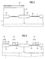
- Fig. 3 shows the substrate 1 after a thin scattering oxide layer 30 has been grown on the substrate and with an ion implantation an n-channel with boron atoms for the NMOSFET has been carried out in the p-well 5 (channel doping not visible).
- the implantation does not go through that Field oxide 20 through, which thus acts as an implantation mask.
- the open area in the n-well 3 also receives the n-implantation. However, this is due to one of the following implantations compensated again.
- An ion implantation with boron follows for the required Channel doping for a p-channel MOS transistor in the n-well (channel doping not visible).
- a gate oxide layer for the gate oxide 40 is first grown on the substrate, then a doped polysilicon layer for the gate electrode 42 is deposited and an insulating layer, for example a TEOS oxide layer, is applied for the gate cover 44.
- the TEOS oxide layer and the polysilicon layer are then structured with a third mask 46, so that a gate oxide 40 and a gate electrode 42 are produced in the sense of the second and third method steps of the method according to the invention (FIG. 4).
- the first silicon oxide spacers 50 are then produced at the edges of the gate electrodes 42 and gate cover 44.
- the first silicon oxide spacers 50 ensure a minimal distance between the gate edge and the source or drain implantation and thus prevent excessive electrical fields on the sides of the gate.
- a scatter oxide is then applied and the area around the n-well 3 is selectively covered with a fourth mask 54 by means of a photoresist 56.
- the open area defines the n-channel transistor region.
- the LDD regions 52 can now be generated in the region of the p-well 5 by means of phosphorus or arsenic implantation.
- the preferred doping material is phosphorus, which is introduced into the substrate with a low energy and a low dose (FIG. 5).
- second silicon oxide spacers 60 are produced, so that they connect to the first silicon oxide spacers 50. Again, the region over the n-well 3 is covered by the fourth mask 54.
- the two implantation steps now follow, which define the source region 59 and the drain region 58 (FIG. 6).
- the first and second implantation steps are carried out directly one after the other and preferably both with arsenic.
- the first implantation step is carried out with a lower energy than the second implantation step.
- the second implantation step leads to an implantation 64 which, because of the higher energy, lies deeper in the substrate than the implantation 62. Superimposed on both concentration profiles results in a flank that slopes gently towards the interior of the substrate.
- the flank falling towards the substrate surface remains unchanged, so that the sheet resistance on the surface of the drain and source is not changed by the second implantation step and the static transistor behavior, for example threshold voltages and characteristic curves, is retained. Accordingly, the transition capacitance C j is reduced without changing the static behavior of the transistors.
- the corresponding implantations for producing the p-channel MOSFET are then carried out.
- a photoresist 78 is used to protect the p-well region 5.
- the first implantation step with BF 2 follows.
- the second implantation step with BF 2 at a higher energy and a lower dose, which leads to a second p-implantation 74. Due to the higher energy of the second implantation step, the second implantation extends deeper into the substrate (FIG. 7).
- the order can be changed here of the first and second implantation steps interchanged become. It should be noted that the p-channel MOSFET in the In contrast to the n-channel MOSFET not with an LDD implantation Is provided. After the implantation, the photoresist 78 etched off and annealing to activate the implanted Boron atoms performed.
- 9 to 13 show the simulated doping profiles in the source / drain area for a 0.2 technology. It shows 9 shows an embodiment without a second implantation step thus belongs to the state of the art. Figures 10 to 13 show four designs according to the invention with different second implantation steps.
- the deepest doping profile is a relatively flat boron doping with a concentration of approximately 1 * 10 17 cm -3 to 1 * 10 18 cm -3 .
- This implantation represents the p-well of the transistor and extends to a depth of approximately 200 nm.
- Two flat implantations were inserted into the p-well: a) a weak doping with phosphorus with an energy of 15 keV and a dose of 2 * 10 13 cm -2 , which defines the LDD region (Lightly-Doped-Drain) . Their maximum is at a depth of about 30 nm with a maximum doping profile of about 1 * 10 19 cm -3 . This implantation essentially serves to reduce the field strength peaks in the edge region of the drain region. b) A strong doping with arsenic with an energy of 30 keV and a dose of 6 * 10 14 cm -2 , which defines the drain and / or source.
- the pn junction between drain / source and well lies at a depth of 70 nm with a doping concentration of approximately 1 * 10 18 cm -3 .
- the relatively high net doping concentration in the vicinity of the pn junction ensures a small depletion zone, which generates a large capacitance C j and thus longer delay times.
- the capacitance C j in this case is 1,143 fF / ⁇ m 2
- the overlap capacitance , C ovl is 0.198 fF / ⁇ m (see Table 1).
- FIG. 10 shows two doping profiles in the source / drain region of an n-channel field effect transistor in accordance with a first embodiment of the invention.
- the boron doping for the p-well and the first implantation step correspond to what was described in connection with FIG. 9.
- the second implantation step was generated with a second energy of 90 keV, which is greater than the first energy, and a second dose of 5 * 10 12 cm -2 , which is smaller than the first dose.
- the larger second energy leads to the fact that the superimposed arsenic doping profile drops less towards the substrate side.
- the pn junction is softer, since the doping edges fall off more weakly and b) the pn junction is at a greater depth, that is to say about 80 nm depth.
- the weakly falling doping flank contributes to the fact that the depletion zone depth in the pn transition region is greater than in FIG. 9. This in turn reduces the pn junction capacity from 1,143 fF / ⁇ m 2 to 1,105 fF / ⁇ m 2 , while the overlap capacity , C ovl , changes only slightly with 0,200 fF / ⁇ m (see Table 1).
- FIG. 11 shows the implantation profiles according to a further embodiment of the invention, in which the second implantation has been carried out with a larger dose, ie 1 * 10 13 cm -2 .
- the pn junction capacitance is therefore only 1,081 fF / ⁇ m 2
- the overlap capacitance , C ovl changes only slightly with 0.201 fF / ⁇ m.
- FIG. 12 shows the implantation profiles according to a further embodiment of the invention, in which the second implantation has been carried out with an energy of 120 keV.
- the higher energy leads to the pn junction being at a depth of 115 nm and the doping flank having a relatively soft drop towards the substrate.
- the resulting greater depletion depth leads to a reduction in the pn junction capacitance to only 0.980 fF / ⁇ m 2 . This is 14% less than the same transistor without a second implantation step , while the overlap capacitance , C ovl , changes only slightly with 0.209 fF / ⁇ m.
- FIG. 13 shows the implantation profiles according to a further embodiment of the invention, in which the second implantation step has been carried out with a dose of 5 * 10 12 cm -2 .
- the pn junction is at a depth of 80 nm. This leads to a reduction in the pn junction capacitance compared to FIG. 9 to 1,042 fF / ⁇ m 2 , while the overlap capacitance , C ovl , is 0.206 fF / ⁇ m changed only marginally.
- Table 1 compares the changes in the capacitance of the pn junction of the described n-channel MOSFETs according to the invention, the table also containing values of designs according to the invention with p-channel field effect transistors (p-channel MOSFETs). (Energy and dose for the second implantation) Substrate Implant.
Landscapes
- Metal-Oxide And Bipolar Metal-Oxide Semiconductor Integrated Circuits (AREA)
- Insulated Gate Type Field-Effect Transistor (AREA)
- Semiconductor Memories (AREA)
Abstract
Es wird ein Verfahren zur Herstellung von Feldeffekttransistoren mit reduzierter pn-Übergangskapazität zwischen Source und/oder Drain und dem Substrat durch Hinzufügen eines zusätzlichen Implantationsschrittes mit hoher Energie und kleiner Dosis bereitgestellt. Die reduzierte pn-Übergangskapazität beschleunigt die Schaltgeschwindigkeit eines Transistors. Beschriebenes Verfahren ist dabei leicht in bestehende Herstellungsverfahren von Feldeffekttransistoren zu integrieren. <IMAGE>
Description
Die vorliegende Erfindung betrifft ein Verfahren zur Herstellung
eines Feldeffekttransistors. Die vorliegende Erfindung
betrifft insbesondere ein Verfahren zur Herstellung von MOS-Feldeffekttransistoren
für integrierte Schaltungen, insbesondere
DRAM- und embedded DRAM-Bauelemente.
Auf dem Weg zu immer schnelleren, hochintegrierten elektronischen
Schaltungen kommt es zunehmend darauf an, die von den
Transistoren verursachten Verzögerungen zu minimieren. Dies
gilt sowohl für analoge Schaltungen als auch für digitale
Schaltungen und Speicher-Bausteine, die meist Feldeffekttransistoren
und insbesondere MOS- oder CMOS-Feldeffekttransistoren
aufweisen.
Die Schaltgeschwindigkeit von Feldeffekttransistoren ist dabei
im wesentlichen durch das Produkt der Lastkapazität des
Transistors (CL), die beim Schalten aufgeladen werden muß,
mit der Versorgungsspannung (Vdd) geteilt durch den Strom Id,
der zum Aufladen verwendet wird, bestimmt. Die Lastkapazität
CL setzt sich dabei aus mehreren parasitären Kapazitäten zusammen,
die je nach der Bauart des Transistors unterschiedlich
stark zu der Lastkapazität betragen. Wichtige Beiträge
zur Lastkapazität sind in der Regel die Kapazität des Gates
zum Substrat (Cg), die Kapazität zwischen Gate und Drain
(Covl), die Kapazität des pn-Übergangs von Drain und/oder
Source zum Substrat (Cj) sowie die Kapazität (Ci), die durch
die Kontakte bedingt sind.
Um die Verzögerungen beim Schalten von Feldeffekttransistoren
gering zu halten, werden nach dem Stand vielfältige Maßnahmen
ergriffen. Zum einen wird versucht, einen möglichst großen
Strom Id bereitzustellen, so dass die Kapazitäten schneller
aufgeladen werden können. Weiterhin werden die Source/Drain-Gebiete
möglichst hoch dotiert, um den Widerstand von Drain
und Source möglichst klein zu haben.
Weitere Maßnahmen bestehen darin, die parasitären Kapazitäten
eines Feldeffekttransistors so gering wie möglich zu gestalten.
Dies geschieht in der Regel dadurch, dass die Gate-Breite
eines Feldeffekttransistors zunehmend reduziert wird,
wodurch sich Cg verkleinert. Jedoch sind die genannten Maßnahmen
weitgehend ausgereizt, so dass sich auf diesem Wege
nur noch mit einem hohen Aufwand eine weitere Reduzierung der
Schaltverzögerungen erzielen läßt.
Der Erfindung liegt daher die Aufgabe zugrunde, ein einfaches
und kostengünstiges Verfahren zur Herstellung eines Feldeffekttransistors
mit erhöhter Schaltgeschwindigkeit bereitzustellen.
Diese Aufgabe wird von dem Verfahren zur Herstellung eines
Feldeffekttransistors gemäß des unabhängigen Patentanspruchs
1 gelöst. Weitere vorteilhafte Ausführungsformen, Ausgestaltungen
und Aspekte der vorliegenden Erfindung ergeben sich
aus den abhängigen Patentansprüchen, der Beschreibung und den
beiliegenden Zeichnungen.
Erfindungsgemäß wird ein Verfahren zur Herstellung eines Feldeffekttransistors
bereitgestellt, das die folgenden Schritten
aufweist:
Der erste Implantationsschritt bezeichnet die Implantation,
die im wesentlichen die Leitfähigkeit von Source und/oder
Drain bestimmt. Sie ist die Implantation mit der höchsten Dosis
im Source und/oder Drain-Gebiet. Sie muß nicht notwendig
die erste Implantation zur Herstellung eines Feldeffekttransistors
oder zur Herstellung von Drain und/oder Source eines
Feldeffekttransistors sein. Mit erstem Implantationsschritt
sind daher nicht Implantationen gemeint, die z.B. eine korrigierende
Funktion in dem Source und/oder Drain-Gebiet ausüben,
wie z.B. die Lightly-Doped-Drain (LDD)-Implantation,
welche die elektrischen Feldspitzen am Rand des Drain-Gebiets
reduzieren.
Das Dotierungsmaterial des ersten Implantationsschrittes kann
aus allen Materialien bestehen, die bzgl. des Substrats den
jeweils anderen Leitungstyp erzeugen; insbesondere also Bor,
wenn das Substrat ein n-Leitungstyp ist oder Phosphor
und/oder Arsen, wenn das Substrat ein p-Leitungstyp ist. Die
Energie, mit der die ionisierten Dotierungsatome oder Moleküle
auf die Oberflächenschicht zu beschleunigt werden, bestimmt
die Tiefe des Dotierungsprofilmaximums und Form des
Dotierungsprofils. Der Implantation folgt normalerweise ein
Wärmebehandlung, so dass die Dotierungsatome weiter in das
Substrat diffundieren und sie im Gitter als Elektronen-Donatoren
oder Elektronen-Akzeptoren aktiviert werden.
Die erste Energie und die erste Dosis beziehen sich auf die
Beschleunigungsenergie und Dosis im ersten Implantationsschritt.
Da die erste Dosis die größte von möglicherweise
mehreren Source und/oder Drain-Implantationen ist, bestimmt
sie im allgemeinen den Schichtwiderstand an der Oberfläche
von Source und/oder Drain.
Der zweite Implantationsschritt erfolgt mit Dotierungsmaterialien
des gleichen Leitungstyps wie im ersten Implantationsschritt,
jedoch mit größerer Energie und kleinerer Dosis.
Ziel dieses Implantationsschrittes ist es, die zum Substratinneren
hin abfallende steile Dotierungsprofilflanke durch
Überlagerung eines zweiten Dotierungsprofils mit niedrigerer
Dosis weniger steil abfallen zu lassen. Auf diese Weise kann
ein weicher pn-Übergang (graded junction) zum Substrat hin
erzeugt werden, der bei gleicher Spannung eine größere Tiefe
der Verarmungszone zwischen Drain/Source und Substrat erzeugt
als ein abruptes Dotierungsprofil. Die größere Verarmungszonentiefe
reduziert die Kapazität zwischen Drain bzw. Source
zum Substrats Cj. Dabei ist es bevorzugt, wenn die Kapazität
des pn-Übergangs vom Source/Drain-Gebiet zu dem Substrat um
mindestens 3%, bevorzugt mindestens 5%, verringert wird.
Das erfindungsgemäße Verfahren hat den Vorteil, dass aufgrund
der größeren Energie und kleineren Dotierung des zweiten Implantationsschrittes
sich das Dotierungsprofil des ersten Implantationsschrittes
von der Oberfläche bis zum Dotierungsprofilmaximum
nur unwesentlich verändert, so dass der
Schichtwiderstandswert von Source und Drain und das statische
Kennlinienverhalten des Feldeffekttransistors weitgehend erhalten
bleiben. Zum Beispiel ist das Short-Channel-Effekt-Verhalten
durch den zweiten Implantationsschritt nicht
beeinflußt. Auch dadurch ist ein einfacher Einbau des erfindungsgemäßen
Verfahrens in eine bestehende Prozessierungslinie
gewährleistet.
Die pn-Übergangskapazität, Cj, kann in hochintegrierten logischen
Schaltungen bis zu 50% der gesamten parasitären Transistorkapazität
ausmachen (siehe IEEE J.Solid State Circuits
SC_19, R.J. Bayuns et al., Seite 755, 1984). Dementsprechend
kann durch erfindungsgemäße Verfahren auf einfache Weise eine
deutliche Reduzierung der Schaltverzögerung eines Feldeffekttransistors
erzielt werden.
Bevorzugt werden der erste und zweite Implantationsschritt
mit der gleichen Maskierung von Drain und/oder Source durchgeführt,
so dass kein zusätzlicher Maskenschritt für den
zweiten Implantationsschritt erforderlich ist. Dies ermöglicht
die Anwendung des erfindungsgemäßen Verfahrens auch auf
einen bestehenden Herstellungsprozeß mit geringem zusätzlichen
Arbeitsaufwand. Bevorzugt werden der erste und der zweite
Implantationsschritt direkt hintereinander durchgeführt,
wobei die Reihenfolge untereinander keine Rolle spielt. Die
Hinzunahme des zweiten Implantationsschrittes stellt in diesem
Fall nur eine relativ geringfügige Änderung eines bestehenden
Herstellungablaufes dar.
In einer bevorzugten Ausführung sind die Dotierungsmaterialien
des ersten Implantationschrittes und des zweiten Implantationschrittes
gleich. Diese Maßgabe ermöglicht ein einfaches
Zusammenlegen des ersten und des zweiten Implantationsschrittes
zu einem einzigen Prozeßschritt, wobei zwischendrin
zum richtigen Zeitpunkt lediglich die Energie von dem Wert
der ersten Energie auf den Wert der zweiten Energie umgestellt
werden muß.
Bevorzugt wird das erfindungsgemäße Verfahren für die Herstellung
von MOS-Feldeffekttransistoren und speziell für die
Herstellung von CMOS-Feldeffekttransistoren, insbesondere für
die Herstellung von embedded DRAMs oder DRAMs angewandt.
Die Erfindung wird nachstehend anhand mehrerer Ausführungsbeispiele
unter Bezugnahme von Zeichnungen dargestellt:
- Fig. 1 - 8
- Erfindungsgemäße Ausführung des Verfahrens zur Herstellung eines n-Kanal- und eines p-Kanal MOS-Feldeffekttransistors.
- Fig. 9 - 13
- Implantationsprofile im Drain/Source-Gebiet eines n-Kanal MOSFETs nach Stand der Technik und nach vier verschiedenen erfindungsgemäßen Ausführungen.
- Fig. 14
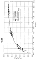
- Vergleich der Schwellenspannungen von n-Kanal MOSFETs nach Stand der Technik und nach vier verschiedenen erfindungsgemäßen Ausführungen für verschiedene Transistor-Kanallängen.
Fig. 1 zeigt ein nach herkömmlichen Verfahren zur Herstellung
von hochintegrierten CMOS-Schaltungen (z.B. im 0.4 µm Prozeß)
bereitgestelltes Substrat 1 aus leicht p-dotiertem Silizium
mit zwei nebeneinanderliegende Gebieten 3 und 5, wobei das
Gebiet 3 durch eine n-Implantation mit Phosphor und das Gebiet
5 durch eine p-Implantation mit Bor erzeugt worden ist.
Das n-implantierte Gebiet 3 wird im folgenden mit n-Wanne und
das p-implantierte Gebiet 5 mit p-Wanne bezeichnet. Durch eine
anschließende Wärmebehandlung diffundieren die Dotierungsatome
der n-Wanne und der p-Wanne in das Substrat 1, so
dass die n- und p-Wannen tiefer in das Substrat hineinreichen
als die anschließenden Implantationen für die noch aufzubringenden
Transistoren.
Auf die Substratoberfläche ist ferner eine Siliziumoxidschicht
7 aufgewachsen, auf der wiederum eine erste Polysiliziumschicht
9 und eine erste Siliziumnitridschicht 11 aufgebracht
ist, die beide auf photolithographischem Wege mit einer
ersten Maske 13 strukturiert worden sind. Die Schichten 9
und 11 definieren die Position zweier Feldeffekttransistoren
dadurch, dass sie bei der folgenden Oxidation den Transistorbereich
abdecken, so dass sich das Feldoxid 20 nur neben den
zu erzeugenden Transistoren bilden kann (Fig.2). Anstelle der
hier gezeigten sogenannten LOCOS-Isolation kann auch eine sogenannte
STI-Isolation (shallow trench isolation) verwendet
werden.
Fig. 3 zeigt das Substrat 1, nachdem eine dünne Streuoxidschicht
30 auf das Substrat aufgewachsen worden ist und mit
einer Ionenimplantation ein n-Kanal mit Bor-Atomen für den
NMOSFET in der p-Wanne 5 durchgeführt worden ist (Kanaldotierung
nicht sichtbar). Die Implantation geht nicht durch das
Feldoxid 20 hindurch, das somit als Implantationsmaske wirkt.
Auch der offene Bereich in der n-Wanne 3 erhält die n-Implantation.
Diese wird jedoch durch eine der folgenden Implantationen
wieder kompensiert. Danach wird mittels einer zweiten
Maske 34 der p-Wannenbereich 5 mit einem Photoresist 32 abgedeckt.
Es folgt eine Ionenimplantation mit Bor für die erforderliche
Kanaldotierung für einen p-Kanal MOS-Transistor in
der n-Wanne (Kanaldotierung nicht sichtbar).
Nach dem Entfernen der Streuoxidschicht 30 wird erst eine Gateoxidschicht
für das Gateoxid 40 auf das Substrat gewachsen,
dann eine dotierte Polysiliziumschicht für die Gate-Elektrode
42 abgeschieden und eine isolierende Schicht , beispielsweise
eine TEOS-Oxidschicht, für die Gate-Abdeckung 44 aufgetragen.
Anschließend werden mit einer dritten Maske 46 die TEOS-Oxidschicht
und die Polysiliziumschicht strukturiert, so dass ein
Gateoxid 40 sowie eine Gate-Elektrode 42 im Sinne des zweiten
und dritten Verfahrensschritts des erfindungsgemäßen Verfahrens
erzeugt werden (Fig. 4).
Anschließend werden an den Rändern der Gate-Elektroden 42 und Gate-Abdeckung 44 die ersten Siliziumoxid-Spacer 50 erzeugt. Die ersten Siliziumoxid-Spacer 50 sorgen für einen minimalen Abstand zwischen Gate-Kante und Source- bzw. Drain-Implantation und verhindern so übergroße elektrische Felder an den Seiten des Gates. Anschließend wird ein Streuoxid aufgebracht und das Gebiet um die n-Wanne 3 mit einer vierten Maske 54 mittels eines Photoresists 56 selektiv abgedeckt. Das offene Gebiet definiert die n-Kanal Transistorregion. Nun können die LDD-Gebiete 52 mittels Phosphor- oder Arsenimplantation im Gebiet der p-Wanne 5 erzeugt werden. Bevorzugtes Dotierungsmaterial ist Phosphor, das mit einer niedrigen Energie und einer geringen Dosis in das Substrat eingebracht wird (Fig. 5).
Anschließend werden an den Rändern der Gate-Elektroden 42 und Gate-Abdeckung 44 die ersten Siliziumoxid-Spacer 50 erzeugt. Die ersten Siliziumoxid-Spacer 50 sorgen für einen minimalen Abstand zwischen Gate-Kante und Source- bzw. Drain-Implantation und verhindern so übergroße elektrische Felder an den Seiten des Gates. Anschließend wird ein Streuoxid aufgebracht und das Gebiet um die n-Wanne 3 mit einer vierten Maske 54 mittels eines Photoresists 56 selektiv abgedeckt. Das offene Gebiet definiert die n-Kanal Transistorregion. Nun können die LDD-Gebiete 52 mittels Phosphor- oder Arsenimplantation im Gebiet der p-Wanne 5 erzeugt werden. Bevorzugtes Dotierungsmaterial ist Phosphor, das mit einer niedrigen Energie und einer geringen Dosis in das Substrat eingebracht wird (Fig. 5).
Anschließend werden zweite Siliziumoxid-Spacer 60 erzeugt, so
dass sich diese an den ersten Siliziumoxid-Spacern 50 anschließen.
Wiederum wird die Region über der n-Wanne 3 mittels
der vierten Maske 54 abgedeckt. Nun folgen die zwei Implantationsschritte,
welche das Source-Gebiet 59 und das
Drain-Gebiet 58 definieren (Fig. 6). Der erste und zweite
Implantationsschritt werden direkt hintereinander und bevorzugt
beide mit Arsen durchgeführt. Der erste Implantationsschritt
wird mit einer niedrigeren Energie als der zweite Implantationsschritt
durchgeführt. Der zweite Implantationsschritt
führt zu einer Implantation 64, die aufgrund der höheren
Energie tiefer im Substrat als die Implantation 62
liegt. Beide Konzentrationsprofile überlagert ergeben eine
zum Substratinneren hin weich abfallende Flanke. Die zur Substratoberfläche
hin abfallende Flanke bleibt unverändert, so
dass der Schichtwiderstand an der Oberfläche von Drain und
Source durch den zweiten Implantationschritt nicht verändert
wird und das statische Transistorverhalten, z.B. Schwellenspannungen
und Kennlinien, erhalten bleibt. Dementsprechend
kommt es zu einer Reduzierung der Übergangskapazität Cj, ohne
dass das statische Verhalten der Transistoren verändert wurde.
Nachfolgend werden die entsprechenden Implantationen zur Erzeugung
des p-Kanal-MOSFETs durchgeführt. Zum Schutz der p-Wannenregion
5 wird ein Photoresist 78 verwendet. Dann folgt
der erste Implantationsschritt mit BF2. Anschließend folgt
der zweite Implantationsschritt mit BF2 bei einer höheren Energie
und einer geringeren Dosis, der zu einer zweiten p-Implantation
74 führt. Aufgrund der höheren Energie des zweiten
Implantationsschrittes reicht die zweite Implantation
tiefer in das Substrat (Fig. 7).
Wie im Falle des n-Kanal MOSFET kann auch hier die Reihenfolge
des ersten und zweiten Implantationsschrittes vertauscht
werden. Es sei bemerkt, dass der p-Kanal MOSFET im
Gegensatz zum n-Kanal MOSFET nicht mit einer LDD-Implantation
ausgestattet ist. Nach der Implantation wird der Photoresist
78 abgeätzt und eine Temperung zur Aktivierung der implantierten
Boratome durchgeführt.
Zum Anschluß der so hergestellten Feldeffekttransistoren wird
nun beispielsweise Titan abgeschieden und getempert, so dass
sich ein selbst-alignierendes Silicide (Salicide) 80 über den
Drain/Source Regionen bilden kann. Der übrige Teil der Titanschicht
wird durch einen Titan-Ätzschritt beseitigt. Schließlich
folgt ein weiterer Temperungsschritt für eine optimale
Barrierenschichtbildung über der Source/Drain-Region. Damit
sind Source- und Drainregionen des P-Kanal Feldeffekttransistors
90 und N-Kanal-Feldeffekttransistor 92 kontaktiert. Es
können jedoch auch andere Kontaktierungsverfahren verwendet
werden. Der weitere Verlauf zur Herstellung einer integrierten
Schaltung mit den erfindungsgemäßen Feldeffekttransistoren
erfolgt mit Methoden nach dem Stand der Technik.
Fig. 9 bis Fig. 13 zeigen die simulierten Dotierungsprofile
im Source/Drain-Bereich für eine 0.2 Technologie. Dabei zeigt
Fig.9 eine Ausführung ohne zweiten Implantationsschritt, die
somit zum Stand der Technik gehört. Die Figuren 10 bis 13
zeigen vier erfindungsgemäße Ausführungen mit verschiedenen
zweiten Implantationsschritten.
Fig. 9 zeigt drei Dotierungsprofile im Source/Drain-Gebiet
eines n-Kanal-Feldeffekttransistors nach Stand der Technik.
Das tiefste Dotierungsprofil ist dabei eine relativ flache
Bor-Dotierung mit einer Konzentration von etwa 1*1017 cm-3 bis
1*1018 cm-3. Diese Implantation repräsentiert die p-Wanne des
Transistors und reicht bis in eine Tiefe von etwa 200 nm.
In die p-Wanne sind zwei flache Implantationen eingefügt worden:
a) eine schwache Dotierung mit Phosphor mit einer Energie
von 15 keV und einer Dosis von 2*1013 cm-2, welche die
LDD-Region (Lightly-Doped-Drain) definiert. Ihr Maximum liegt
in einer Tiefe von etwa 30 nm mit einem Dotierungsprofilmaximum
von etwa 1*1019 cm-3. Diese Implantation dient im wesentlichen
dazu die Feldstärkenspitzen in der Randregion Draingebiets
zu reduzieren. b) Eine starke Dotierung mit Arsen mit
einer Energie von 30 keV und einer Dosis von 6*1014 cm-2, welche
die Drain und/oder Source definiert. Ihr Maximum liegt in
einer Tiefe von etwa 35 nm mit einem Maximum des Dotierungsprofils
von etwa 3*1020 cm-2. Durch die Bildung eines Spacers
an den Seitenwänden der Gateelektrode sind diese beiden Implantationen
zueinander lateral versetzt angeordnet. Die
Phosphor-Implantation spielt für die folgenden Erläuterungen
keine Rolle. Daher diese Implantation in den Figuren 10 bis
13 nicht mehr gezeigt.
Der pn-Übergang zwischen Drain/Source und Wanne liegt in einer
Tiefe von 70 nm bei einer Dotierungskonzentration von etwa
1*1018 cm-3. Die relativ hohe Netto-Dotierungskonzentration
in der in der Nähe des pn-Übergangs sorgt für eine kleine
Verarmungszone, die eine große Kapazität Cj und damit größere
Verzögerungszeiten erzeugt. Die Kapazität Cj beträgt in diesem
Fall 1.143 fF/µm2, und die Überlappungskapazität, Covl,
beträgt 0.198 fF/µm (siehe Tabelle 1).
Fig. 10 zeigt zwei Dotierungsprofile im Source/Drain-Gebiet
eines n-Kanal-Feldeffekttransistors entsprechend einer ersten
Ausführungsform der Erfindung. Die Bor-Dotierung für die p-Wanne
und der ersten Implantationsschritt entsprechen dem,
was im Zusammenhang mit Fig. 9 beschrieben wurden. Der zweite
Implantationsschritt ist mit einer zweiten Energie von 90
keV, die größer ist als die erste Energie, und einer zweiten
Dosis von 5*1012 cm-2, die kleiner ist als die erste Dosis,
erzeugt worden. Die größere zweite Energie führt dazu, dass
das überlagerte Arsen-Dotierungsprofil zur Substratseite hin
schwächer abfällt. Das führt dazu, dass a) der pn-Übergang
weicher ist, da die Dotierungsflanken schwächer abfallen und
b) der pn-Übergang in größerer Tiefe, d.h. in etwa 80 nm Tiefe
liegt. Insbesondere die schwächer abfallende Dotierungsflanke
trägt dazu bei, dass die Verarmungszonentiefe im
pn-Übergangsbereich größer als in Fig. 9 ist. Das wiederum
reduziert die pn-Übergangskapazität von 1.143 fF/µm2 auf
1.105 fF/µm2, während die Überlappungskapazität, Covl, sich
mit 0.200 fF/µm nur unwesentlich verändert (siehe Tabelle 1).
Fig. 11 zeigt die Implantationsprofile nach einer weiteren
Ausführung der Erfindung, bei welcher die zweite Implantation
mit einer größeren Dosis, d.h. 1*1013 cm-2, durchgeführt worden
ist. Dies führt dazu, dass der pn-Übergang in einer Tiefe
von 95 nm liegt und die Dotierungsflanke nochmals schwächer
zum Substrat hin abfällt. Die pn-Übergangskapazität ist daher
nur 1.081 fF/µm2, während die Überlappungskapazität, Covl,
sich mit 0.201 fF/µm nur unwesentlich verändert.
Fig. 12 zeigt die Implantationsprofile nach einer weiteren
Ausführung der Erfindung, bei welcher die zweite Implantation
mit einer Energie von 120 keV durchgeführt worden ist. Die
höhere Energie führt dazu, dass der pn-Übergang in einer Tiefe
von 115 nm liegt und die Dotierungsflanke einen relativ
weichen Abfall zum Substrat hin aufweist. Die daraus folgende
größere Verarmungstiefe führt zu einer Reduzierung der pn-Übergangskapazität
auf nur 0.980 fF/µm2. Das sind 14% weniger
als der gleiche Transistor ohne zweiten Implantationsschritt,
während die Überlappungskapazität, Covl, sich mit 0.209 fF/µm
nur unwesentlich verändert.
Fig. 13 zeigt die Implantationsprofile nach einer weiteren
Ausführung der Erfindung, bei welcher der zweite Implantationsschritt
mit einer Dosis von 5*1012 cm-2 durchgeführt worden
ist. Der pn-Übergang liegt in diesem Fall in einer Tiefe von
80 nm. Dies führt zu einer Reduzierung der pn-Übergangskapazität
gegenüber Fig.9 auf 1.042 fF/µm2, während die Überlappungskapazität,
Covl, sich mit 0.206 fF/µm nur unwesentlich
verändert.
Fig. 14 zeigt eine Untersuchung der Schwellenspannungen von
n-Kanal Feldeffekttransistoren, die nach dem Stand der Technik
mit Implantationsparametern wie in Fig. 9 und nach erfindungsgemäßen
Ausführungen mit Implantationsparametern wie in
Fig. 10 bis Fig. 13 hergestellt worden sind. Diese Untersuchungen
wurden mit verschiedenen effektiven Transistor-Kanallängen,
Leff, zwischen 150 nm und 350 nm durchgeführt. Die
Untersuchung zeigt, dass der Abfall der Schwellenspannung bei
sehr kurzer effektiver Kanallängen weitestgehend unabhängig
davon ist, ob und mit welchen Energien und Dosis' der zweite
Implantationsschritt durchgeführt worden ist. Dies ist ein
wichtiger Nachweis für Kompatibilität des zweiten Implantationsschrittes
mit herkömmlichen Verfahren, so dass das erfindungsgemäße
Verfahren ohne großen Aufwand in ein bestehendes
Verfahren zur Herstellung von Feldeffekttransistoren verwandt
werden kann.
Tabelle 1 vergleicht die Veränderungen der Kapazitäten des
pn-Übergangs der beschriebenen, erfindungsgemäßen n-Kanal
MOSFETs, wobei die Tabelle auch Werte von erfindungsgemäßen
Ausführungen mit p-Kanal Feldeffekttransistoren (p-Kanal MOSFETs)
enthält.
| (Energie und Dosis für die zweite Implantation) | ||||||
| Substrat | Implant. | Energie (keV) | Dosis (cm-2) | Cj (fF/µm2) | Covl (fF/µm) | |
| NMOS | Bor | As | 0 | 0 | 1.143 | 0.198 |
| NMOS | Bor | As | 90 | 5*1012 | 1.105 | 0.200 |
| NMOS | Bor | As | 90 | 1*1013 | 1.081 | 0.201 |
| NMOS | Bor | As | 120 | 1*1013 | 0.980 | 0.209 |
| NMOS | Bor | As | 120 | 5*1012 | 1.042 | 0.206 |
| PMOS | P | BF2 | 0 | 0 | 1.427 | 0.263 |
| PMOS | P | BF2 | 60 | 5*1012 | 1.361 | 0.266 |
| PMOS | P | BF2 | 60 | 1*1013 | 1.304 | 0.281 |
| PMOS | P | BF2 | 80 | 1*1013 | 1.161 | 0.279 |
| PMOS | P | BF2 | 80 | 5*1012 | 1.289 | 0.276 |
- 1
- Halbleitersubstrat
- 3
- n-Wanne
- 5
- p-Wanne
- 7
- Siliziumoxid
- 9
- Polysiliziumschicht
- 11
- Siliziumnitridschicht
- 13
- Maske
- 20
- Feldoxid
- 30
- Streuoxid
- 32
- Photoresist
- 34
- Maske
- 40
- Gateoxid
- 42
- Gateelektrode
- 44
- TEOS-Oxid
- 46
- Maske
- 50
- Spacer
- 52
- LDD-Gebiet
- 54
- Maske
- 56
- Photoresist
- 58
- Drain-Gebiet
- 59
- Source-Gebiet
- 60
- Spacer
- 62
- Implatation
- 64
- Implantation
- 72
- Implantation
- 74
- Implantation
- 76
- Maske
- 78
- Photoresist
- 80
- Salicide
- 90
- p-FET
- 92
- n-FET
Claims (6)
- Verfahren zur Herstellung eines Feldeffekttransistors mit den Schritten:a) ein Substrat, das eine Oberflächenschicht aus einem Material eines ersten Leitungstyps aufweist, wird bereitgestellt;b) ein Gateoxid wird erzeugt;c) eine Gate-Elektrode wird aufgebracht;d) ein erster Implantationsschritt zur Erzeugung der Source/Drain-Gebiete wird mit einem Dotierungsmaterial des zweiten Leitungstyps, mit einer ersten Energie und einer ersten Dosis durchgeführt; unde) ein zweiter Implantationsschritt wird mit einem Dotierungsmaterial des zweiten Leitungstyps, mit einer zweiten Energie und einer zweiten Dosis durchgeführt, wobei die zweite Energie größer als die erste Energie und die zweite Dosis kleiner als die erste Dosis ist, so dass die Kapazität des pn-Übergangs vom Source/Drain-Gebiet zu dem Substrat verringert wird.
- Verfahren nach Anspruch 1,
dadurch gekennzeichnet, dass
die Kapazität des pn-Übergangs vom Source/Drain-Gebiet zu dem Substrat um mindestens 3%, bevorzugt mindestens 5%, verringert wird. - Verfahren nach Anspruch 1 oder 2,
dadurch gekennzeichnet, dass
die Maskierung von Drain und/oder Source für den ersten und den zweiten Implantationsschritt gleich ist. - Verfahren nach einem der Ansprüche 1 bis 3,
dadurch gekennzeichnet, dass
die Dotierungsmaterialien des ersten Implantationsschritts und des zweiten Implantationsschritts gleich sind. - Verfahren nach einem der Ansprüche 1 bis 4,
dadurch gekennzeichnet, dass
das Verfahren für die Herstellung von integrierten Schaltungen mit CMOS-Feldeffekttransistoren verwandt wird. - Verfahren nach Anspruch 5,
dadurch gekennzeichnet, dass
die integrierten Schaltungen Embedded DRAM oder DRAMs sind.
Applications Claiming Priority (2)
| Application Number | Priority Date | Filing Date | Title |
|---|---|---|---|
| DE10029659 | 2000-06-16 | ||
| DE10029659A DE10029659A1 (de) | 2000-06-16 | 2000-06-16 | Verfahren zur Herstellung eines Feldeffekttransistors |
Publications (1)
| Publication Number | Publication Date |
|---|---|
| EP1164634A2 true EP1164634A2 (de) | 2001-12-19 |
Family
ID=7645938
Family Applications (1)
| Application Number | Title | Priority Date | Filing Date |
|---|---|---|---|
| EP01114016A Withdrawn EP1164634A2 (de) | 2000-06-16 | 2001-06-08 | Verfahren zur Herstellung eines Feldeffekttransistors |
Country Status (5)
| Country | Link |
|---|---|
| US (1) | US20020039819A1 (de) |
| EP (1) | EP1164634A2 (de) |
| JP (1) | JP2002050639A (de) |
| KR (1) | KR20010113510A (de) |
| DE (1) | DE10029659A1 (de) |
Families Citing this family (4)
| Publication number | Priority date | Publication date | Assignee | Title |
|---|---|---|---|---|
| FR2794898B1 (fr) | 1999-06-11 | 2001-09-14 | France Telecom | Dispositif semi-conducteur a tension de seuil compensee et procede de fabrication |
| JP4122167B2 (ja) * | 2002-03-19 | 2008-07-23 | 富士通株式会社 | 半導体装置及びその製造方法 |
| JP2007298190A (ja) * | 2006-04-27 | 2007-11-15 | Noritz Corp | 燃焼装置 |
| DE102013104019B4 (de) * | 2012-10-15 | 2015-02-12 | Taiwan Semiconductor Mfg. Co., Ltd. | Verfahren und Struktur zur Steigerung der Leistungsfähigkeit und der Minderung der NBTI (Negative Bias Temperature Instability) eines MOSFET |
Family Cites Families (3)
| Publication number | Priority date | Publication date | Assignee | Title |
|---|---|---|---|---|
| US5028556A (en) * | 1990-02-16 | 1991-07-02 | Hughes Aircraft Company | Process for fabricating radiation hard high voltage devices |
| JPH0653232A (ja) * | 1992-08-03 | 1994-02-25 | Mitsubishi Electric Corp | 半導体装置およびその製造方法 |
| US5952693A (en) * | 1997-09-05 | 1999-09-14 | Advanced Micro Devices, Inc. | CMOS semiconductor device comprising graded junctions with reduced junction capacitance |
-
2000
- 2000-06-16 DE DE10029659A patent/DE10029659A1/de not_active Ceased
-
2001
- 2001-06-08 EP EP01114016A patent/EP1164634A2/de not_active Withdrawn
- 2001-06-15 KR KR1020010033917A patent/KR20010113510A/ko not_active Ceased
- 2001-06-18 US US09/883,821 patent/US20020039819A1/en not_active Abandoned
- 2001-06-18 JP JP2001183760A patent/JP2002050639A/ja active Pending
Also Published As
| Publication number | Publication date |
|---|---|
| US20020039819A1 (en) | 2002-04-04 |
| KR20010113510A (ko) | 2001-12-28 |
| DE10029659A1 (de) | 2002-01-03 |
| JP2002050639A (ja) | 2002-02-15 |
Similar Documents
| Publication | Publication Date | Title |
|---|---|---|
| DE69615458T2 (de) | Dünnfilmtransistor über einem isolierten Halbleitersubstrat und Verfahren zur Herstellung | |
| DE69522139T2 (de) | Verfahren zur Herstellung einer CMOS Vorrichtung | |
| DE10297679B4 (de) | Dotierverfahren für vollständig verarmte SOI-Strukturen | |
| DE60213889T2 (de) | Halbleiteranordnung | |
| DE69525188T2 (de) | Hoch- und Niederspannungs-CMOS-Bauteil und Herstellungsverfahren | |
| DE68926985T2 (de) | Verfahren zum Herstellen einer Halbleiteranordnung mit einem Siliziumkörper, in dem durch Ionenimplantationen Halbleitergebiete gebildet werden | |
| DE69129430T2 (de) | Verfahren zum Herstellen von MOS-Anordnungen in VLSI-Strukturen | |
| DE69432918T2 (de) | Verfahren zum Herstellen eines CMOS-Bauteil mit Hoch- und Niedrigspannungstransistoren | |
| DE68928326T2 (de) | Eingeschlossener transistor mit eingegrabenem kanal | |
| DE19642538A1 (de) | Halbleitereinrichtung und Herstellungsverfahren derselben | |
| DE69524050T2 (de) | Gegenimplantationsverfahren bei der herstellung einer halbleitervorrichtung mit selbstausrichtenden ''anti-punchthrough''-gebieten | |
| DE102005022129B4 (de) | Feldeffekttransistor und Verfahren zum Herstellen eines Feldeffekttransistors | |
| DE69836941T2 (de) | Herstellungsverfahren für MOS-Struktur mit asymetrisch-dotiertem Kanal | |
| DE102004018153B4 (de) | Hochvolt-Sperrschicht-Feldeffekttransistor mit retrograder Gatewanne und Verfahren zu dessen Herstellung | |
| DE69736971T2 (de) | Herstellungsverfahren einer integrierten leistungsschaltungsanordnung | |
| DE19612950C1 (de) | Schaltungsstruktur mit mindestens einem MOS-Transistor und Verfahren zu deren Herstellung | |
| DE4112044A1 (de) | Halbleitereinrichtung mit wenigstens zwei feldeffekttransistoren und herstellungsverfahren fuer diese | |
| DE10245608A1 (de) | Halbleiterelement mit verbesserten Halo-Strukturen und Verfahren zur Herstellung der Halo-Strukturen eines Halbleiterelements | |
| DE102006019936B4 (de) | Halbleiterbauelement mit unterschiedlich verspannten Ätzstoppschichten in Verbindung mit PN-Übergängen unterschiedlicher Gestaltung in unterschiedlichen Bauteilgebieten und Verfahren zur Herstellung des Halbleiterbauelements | |
| DE69519016T2 (de) | Hochspannungs-ldd-mosfet mit erhöhter durchbruchspannung und herstellungsverfahren | |
| EP1164634A2 (de) | Verfahren zur Herstellung eines Feldeffekttransistors | |
| DE102004063144A1 (de) | Halbleiter-Bauelement und Herstellungsverfahren dafür | |
| DE19952742C2 (de) | Halbleiterspeicher-Bauelement, insbesondere ein SRAM, und Verfahren zu seiner Herstellung | |
| WO2007033692A1 (de) | Hochvolttransistor und verfahren zu seiner herstellung | |
| DE102004014928B4 (de) | Hochvolttransistor und Verfahren zu seiner Herstellung |
Legal Events
| Date | Code | Title | Description |
|---|---|---|---|
| PUAI | Public reference made under article 153(3) epc to a published international application that has entered the european phase |
Free format text: ORIGINAL CODE: 0009012 |
|
| AK | Designated contracting states |
Kind code of ref document: A2 Designated state(s): AT BE CH CY DE DK ES FI FR GB GR IE IT LI LU MC NL PT SE TR |
|
| AX | Request for extension of the european patent |
Free format text: AL;LT;LV;MK;RO;SI |
|
| STAA | Information on the status of an ep patent application or granted ep patent |
Free format text: STATUS: THE APPLICATION IS DEEMED TO BE WITHDRAWN |
|
| 18D | Application deemed to be withdrawn |
Effective date: 20031231 |