EP1162832A2 - Verfahren und Vorrichtung zur Korrektur der Nicht-Uniformität von abgetasteten Digitalbildern - Google Patents
Verfahren und Vorrichtung zur Korrektur der Nicht-Uniformität von abgetasteten Digitalbildern Download PDFInfo
- Publication number
- EP1162832A2 EP1162832A2 EP01201950A EP01201950A EP1162832A2 EP 1162832 A2 EP1162832 A2 EP 1162832A2 EP 01201950 A EP01201950 A EP 01201950A EP 01201950 A EP01201950 A EP 01201950A EP 1162832 A2 EP1162832 A2 EP 1162832A2
- Authority
- EP
- European Patent Office
- Prior art keywords
- uniformity
- pixel
- correction
- raster scan
- pixel regions
- Prior art date
- Legal status (The legal status is an assumption and is not a legal conclusion. Google has not performed a legal analysis and makes no representation as to the accuracy of the status listed.)
- Withdrawn
Links
Images


Classifications
-
- H—ELECTRICITY
- H04—ELECTRIC COMMUNICATION TECHNIQUE
- H04N—PICTORIAL COMMUNICATION, e.g. TELEVISION
- H04N3/00—Scanning details of television systems; Combination thereof with generation of supply voltages
- H04N3/36—Scanning of motion picture films, e.g. for telecine
-
- H—ELECTRICITY
- H04—ELECTRIC COMMUNICATION TECHNIQUE
- H04N—PICTORIAL COMMUNICATION, e.g. TELEVISION
- H04N1/00—Scanning, transmission or reproduction of documents or the like, e.g. facsimile transmission; Details thereof
- H04N1/40—Picture signal circuits
- H04N1/401—Compensating positionally unequal response of the pick-up or reproducing head
- H04N1/4015—Compensating positionally unequal response of the pick-up or reproducing head of the reproducing head
-
- H—ELECTRICITY
- H04—ELECTRIC COMMUNICATION TECHNIQUE
- H04N—PICTORIAL COMMUNICATION, e.g. TELEVISION
- H04N25/00—Circuitry of solid-state image sensors [SSIS]; Control thereof
- H04N25/60—Noise processing, e.g. detecting, correcting, reducing or removing noise
- H04N25/67—Noise processing, e.g. detecting, correcting, reducing or removing noise applied to fixed-pattern noise, e.g. non-uniformity of response
- H04N25/671—Noise processing, e.g. detecting, correcting, reducing or removing noise applied to fixed-pattern noise, e.g. non-uniformity of response for non-uniformity detection or correction
-
- H—ELECTRICITY
- H04—ELECTRIC COMMUNICATION TECHNIQUE
- H04N—PICTORIAL COMMUNICATION, e.g. TELEVISION
- H04N5/00—Details of television systems
- H04N5/222—Studio circuitry; Studio devices; Studio equipment
- H04N5/253—Picture signal generating by scanning motion picture films or slide opaques, e.g. for telecine
Definitions
- the present invention relates to raster scan recording of motion picture film in general, and to correcting system-introduced scan line non-uniformities in particular.
- raster scan motion picture recording involves for each frame, exposing moving film to a focused, oscillating writing beam at discrete locations ("pixels") along a series of scan lines that are perpendicular to the direction of film travel.
- pixels discrete locations
- three primary color (e.g., red, blue and green, or yellow, cyan and magenta) writing beams are converged at each pixel location, with the relative beam intensities, controlled by light modulators, determining the perceived color and density of the pixel on the recording medium.
- Figure 1 is an exaggerated example of an image having horizontal non-uniformity. Undulatory vertical stripe regions of noticeably different light intensities characterize horizontal non-uniformity.
- a raster scan film recorder having significant horizontal non-uniformity reproduces similar undesirable artifacts in all scan lines of the images produced.
- the present invention provides, in raster scan film recording, a method of correcting system-generated image non-uniformities.
- the method at least includes the steps of: establishing at least one correction axis for correcting non-uniformity in pixels substantially aligned with the correction axis; correcting endemic non-uniformity of pixel regions along the correction axis, the pixel regions at least including one image pixel, based upon the position of the pixel regions along the correction axis; and correcting endemic non-uniformity of the pixel regions along the correction axis, based upon the intensity of the pixel regions.
- the present invention also provides an apparatus for correcting system-generated image non-uniformities in raster scan film recording.
- the apparatus at least includes a position-based non-uniformity corrector adapted to correct endemic non-uniformity of pixel regions along at least one established correction axis, the pixel regions at least including one image pixel, based upon the position of the pixel regions along the correction axis.
- the apparatus also at least includes an intensity-based non-uniformity corrector adapted to correct endemic non-uniformity of the pixel regions along the correction axis, based upon the intensity of the pixel regions.
- the present-inventive non-uniformity correction method and apparatus for the correction of horizontal line non-uniformity and the like novelly provides for non-uniformity-corrected pixel data, taking into account both the position of the pixel on the scan line, and the intensity data of the incoming pixel. This results in an image code that is not only corrected for the horizontal position along the scan lines, but also for the signal level of each pixel or pixel group.
- the present invention is implemented via one of the film calibration and line non-uniformity correction circuits 200 or 300.
- a film calibration table 202 under direction of system control (not shown) is responsible for transforming data from incoming pixels to a form compatible with the light modulators (also not shown).
- the film-calibrated data is then corrected for line non-uniformity by a line non-uniformity corrector 206.
- a digital-to-analog converter 210 then converts the corrected pixel data, before outputting (at 212) it to the light modulators.
- the system 300 performs the same function as the system 200, but with the line non-uniformity correction occurring before film calibration. Whether the system 200 or the 300 is used to correct line non-uniformities according to the present invention, is a matter of design choice.
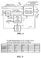
- Figure 4 shows a schematic block diagram of the present-inventive line non-uniformity corrector 206.
- digital pixel data received via a digital pixel data bus 402 is applied to a look up table 404.
- the output of the look up table 404 via a corrected digital pixel data output bus 412 is presented to the digital-to-analog converter 210 for later presentation to the light modulators.
- the pixel number in the scan line output by a pixel counter 408 via a pixel number bus is combined with the data value from the digital pixel data bus 402.
- a reference pixel clock signal introduced via line 406 synchronizes the operation of the line non-uniformity corrector 206.
- An image processor and controller bus interface 416 controls the overall operation of the corrector.
- the image processor and controller bus interface 416 At the beginning of a scan line, triggered by a line start signal at input 414, the image processor and controller bus interface 416 resets the pixel counter 408 to begin counting the pixel positions along a scan line. The pixel counter is incremented each time a pixel clock signal is received. The image processor and controller bus interface 416 also triggers the look up table 404 to read out the appropriate corrected digital pixel data for each pixel location.
- the pixel clock signal also synchronizes other operations of the raster scan film recording process, it is output via line 420 from the line non-uniformity corrector.
- a pixel clock delay line 418 introduces a delay to compensate for the latency associated with acquiring data from the look up table 404, so that the corrected digital pixel data is output simultaneously with the pixel clock signal.
- Figure 5 details a sample line non-uniformity look up table for correcting the pixel data of one writing beam color.
- the look up table 404 contains either three look up tables such as the example in Figure 5, or a large combined look up table with the values for three colors. From Figure 5, and in accordance with the present invention, there is a pixel data entry for every horizontal pixel position, and for every pixel intensity level possible.
- corrected pixel data can be stored not for each pixel, but rather for each predefined group of pixels.
- the group can be chosen based upon the assumption that line non-uniformities do not drastically change from pixel to pixel. For example, if the pixel group contains 8 pixels, then only 6,291,456 entries are required for a comprehensive line non-uniformity look up table ⁇ a reduction of more than 44 million entries.
- the present invention is not limited to correction of non-uniformities along the scan lines, but may also be used to correct vertical non-uniformities.
- the present invention can also be used to correct both horizontal and vertical non-uniformities by storing an entry for every pixel in the entire image, or at least an entry for every grouping of pixels throughout the entire image.
- look up table and line non-uniformity corrector of the present invention can be implemented and numerous ways, using any combination of the following: software, hardware (including stand-alone systems, as well as networked systems), and firmware.
Landscapes
- Engineering & Computer Science (AREA)
- Multimedia (AREA)
- Signal Processing (AREA)
- Facsimile Image Signal Circuits (AREA)
- Facsimile Scanning Arrangements (AREA)
Applications Claiming Priority (4)
| Application Number | Priority Date | Filing Date | Title |
|---|---|---|---|
| US20964500P | 2000-06-06 | 2000-06-06 | |
| US209645P | 2000-06-06 | ||
| US758823 | 2001-01-11 | ||
| US09/758,823 US20020126199A1 (en) | 2000-06-06 | 2001-01-11 | Method and apparatus for correcting non-uniformity in digital images created on a raster scan film recorder |
Publications (2)
| Publication Number | Publication Date |
|---|---|
| EP1162832A2 true EP1162832A2 (de) | 2001-12-12 |
| EP1162832A3 EP1162832A3 (de) | 2006-05-17 |
Family
ID=26904343
Family Applications (1)
| Application Number | Title | Priority Date | Filing Date |
|---|---|---|---|
| EP01201950A Withdrawn EP1162832A3 (de) | 2000-06-06 | 2001-05-25 | Verfahren und Vorrichtung zur Korrektur der Nicht-Uniformität von abgetasteten Digitalbildern |
Country Status (2)
| Country | Link |
|---|---|
| US (1) | US20020126199A1 (de) |
| EP (1) | EP1162832A3 (de) |
Families Citing this family (1)
| Publication number | Priority date | Publication date | Assignee | Title |
|---|---|---|---|---|
| US6917758B1 (en) * | 2003-12-19 | 2005-07-12 | Eastman Kodak Company | Method of image compensation for watermarked film |
Family Cites Families (4)
| Publication number | Priority date | Publication date | Assignee | Title |
|---|---|---|---|---|
| US4751523A (en) * | 1986-06-30 | 1988-06-14 | Xerox Corporation | Laser scanner power compensation circuit |
| EP0486311B1 (de) * | 1990-11-15 | 2001-10-10 | Canon Kabushiki Kaisha | Farbbildverarbeitungsgerät und -verfahren |
| US5359431A (en) * | 1992-06-05 | 1994-10-25 | Eastman Kodak Company | Classification to change exposure within a cell of different pixels |
| US5493322A (en) * | 1993-04-01 | 1996-02-20 | Eastman Kodak Company | Electrophotographic image forming apparatus with non-uniformity correction of recording elements |
-
2001
- 2001-01-11 US US09/758,823 patent/US20020126199A1/en not_active Abandoned
- 2001-05-25 EP EP01201950A patent/EP1162832A3/de not_active Withdrawn
Also Published As
| Publication number | Publication date |
|---|---|
| EP1162832A3 (de) | 2006-05-17 |
| US20020126199A1 (en) | 2002-09-12 |
Similar Documents
| Publication | Publication Date | Title |
|---|---|---|
| US6814448B2 (en) | Image projection and display device | |
| KR100188218B1 (ko) | 투사형 화상표시시스템의 비대칭화면 보정위치제어 방법 | |
| JP4136040B2 (ja) | ロード/リセット・シーケンスを自動的に供給する方法 | |
| US20080136763A1 (en) | Image processing apparatus, image processing method, display apparatus, and projection display apparatus | |
| EP1137255B1 (de) | Korrekturverfahren und -vorrichtung für Bildsignale die durch einen Bildsensor mit mehreren Ausgangskanälen erzeugt wurden | |
| GB2473393A (en) | Projector and method for projecting an image | |
| EP1251461A2 (de) | Verfahren zum Kompensieren des Lichtabfalls eines digitalen Bildes bei minimaler Änderung des Lichtgleichgewichts | |
| JPS6184161A (ja) | カラ−印刷用デ−タを発生させる方法および装置 | |
| US5153732A (en) | Electronic still camera which reduces the influence of smear and dark current | |
| JPS643393B2 (de) | ||
| US7460275B2 (en) | Odd/even error diffusion filter | |
| EP1162832A2 (de) | Verfahren und Vorrichtung zur Korrektur der Nicht-Uniformität von abgetasteten Digitalbildern | |
| EP0420152B1 (de) | Verfahren und Vorrichtung zur Beseitigung von Falschbildern | |
| JP2002108298A (ja) | デジタル信号処理回路およびその処理方法、並びに表示装置、液晶表示装置および液晶プロジェクタ | |
| US8508672B2 (en) | System and method for improving video image sharpness | |
| US5303056A (en) | Dynamic gain correction for CRT printing | |
| JP2001197332A (ja) | 画像再生システムの欠陥を判定し且つ少なくとも部分的に補正する方法及び該方法を実施するための装置 | |
| JP2000180779A (ja) | プロジェクタ装置 | |
| JP2002218186A (ja) | 撮像装置及び画像信号の調整方法 | |
| US5748341A (en) | Method of and apparatus for determining whether an original is present in a readout region | |
| WO1991010315A1 (en) | Electronic film editing | |
| JP3276026B2 (ja) | 画像読み取り装置の画像データ調整方法 | |
| JP3557833B2 (ja) | 映像表示装置 | |
| JPS6163177A (ja) | デイジタルコンバ−ゼンス装置 | |
| WO2025220471A1 (ja) | 投写型映像表示装置 |
Legal Events
| Date | Code | Title | Description |
|---|---|---|---|
| PUAI | Public reference made under article 153(3) epc to a published international application that has entered the european phase |
Free format text: ORIGINAL CODE: 0009012 |
|
| AK | Designated contracting states |
Kind code of ref document: A2 Designated state(s): AT BE CH CY DE DK ES FI FR GB GR IE IT LI LU MC NL PT SE TR |
|
| AX | Request for extension of the european patent |
Free format text: AL;LT;LV;MK;RO;SI |
|
| PUAL | Search report despatched |
Free format text: ORIGINAL CODE: 0009013 |
|
| AK | Designated contracting states |
Kind code of ref document: A3 Designated state(s): AT BE CH CY DE DK ES FI FR GB GR IE IT LI LU MC NL PT SE TR |
|
| AX | Request for extension of the european patent |
Extension state: AL LT LV MK RO SI |
|
| AKX | Designation fees paid | ||
| REG | Reference to a national code |
Ref country code: DE Ref legal event code: 8566 |
|
| STAA | Information on the status of an ep patent application or granted ep patent |
Free format text: STATUS: THE APPLICATION IS DEEMED TO BE WITHDRAWN |
|
| 18D | Application deemed to be withdrawn |
Effective date: 20061118 |