EP1160909A2 - Dual mode band-pass filter - Google Patents
Dual mode band-pass filter Download PDFInfo
- Publication number
- EP1160909A2 EP1160909A2 EP01111070A EP01111070A EP1160909A2 EP 1160909 A2 EP1160909 A2 EP 1160909A2 EP 01111070 A EP01111070 A EP 01111070A EP 01111070 A EP01111070 A EP 01111070A EP 1160909 A2 EP1160909 A2 EP 1160909A2
- Authority
- EP
- European Patent Office
- Prior art keywords
- pass filter
- dual mode
- dielectric body
- metal film
- mode band
- Prior art date
- Legal status (The legal status is an assumption and is not a legal conclusion. Google has not performed a legal analysis and makes no representation as to the accuracy of the status listed.)
- Granted
Links
Images

Classifications
-
- H—ELECTRICITY
- H01—ELECTRIC ELEMENTS
- H01P—WAVEGUIDES; RESONATORS, LINES, OR OTHER DEVICES OF THE WAVEGUIDE TYPE
- H01P7/00—Resonators of the waveguide type
- H01P7/08—Strip line resonators
- H01P7/082—Microstripline resonators
-
- H—ELECTRICITY
- H01—ELECTRIC ELEMENTS
- H01P—WAVEGUIDES; RESONATORS, LINES, OR OTHER DEVICES OF THE WAVEGUIDE TYPE
- H01P7/00—Resonators of the waveguide type
- H01P7/08—Strip line resonators
- H01P7/084—Triplate line resonators
Definitions
- the present invention relates to a dual mode band-pass filter used, for example, as a band filter in a communication apparatus operating in a band that ranges from the microwave band to the millimeter wave band.
- the present invention relates to a dual mode band-pass filter having an improved dielectric body.
- FIGs. 5 and 6 are schematic diagrams showing conventional dual mode band-pass filters.
- a circular conductive film 201 is provided on a dielectric body (not shown in the drawing).
- An input-output coupling circuit 202 and an input-output coupling circuit 203 are coupled with the conductive film 201 and are arranged to be perpendicular to each other.
- An open-top stub 204 is arranged to be at a central angle of 45° with respect to the input-output coupling circuit 203.
- a substantially square conductive film 211 is provided on a dielectric body.
- Input-output coupling circuits 212 and 213 are coupled with the conductive film 211 and are arranged to be perpendicular to each other.
- a chamfered section 211a being provided, two resonant modes have different resonant frequencies, and the two resonant modes are combined so that the band-pass filter 210 functions as a dual mode band-pass filter.
- dual mode filters using ring-shaped conductive films instead of circular conductive films are also known, as disclosed in Japanese Unexamined Patent Application Publication Nos. 9-139612 and 9-162610. That is, in such a dual mode filter, a ring transmission line is used, and in a manner similar to that in the dual mode band-pass filter shown in FIG. 5, input-output coupling circuits are arranged to be perpendicular to each other, and also an open-top stub is provided on a portion of the ring transmission line.
- Japanese Unexamined Patent Application Publication No. 6-112701 also discloses a dual mode filter using a similar ring transmission line.
- the dielectric body for example, a BAS body containing BaO, Al 2 O 5 , and SiO 2 as main constituents, or a body composed of a synthetic resin is used.
- the band-pass filter by forming one conductive film pattern, a double band-pass filter can be constructed, and thus the band-pass filter can be miniaturized.
- the dielectric loss of the dielectric body i.e., the Q value of the dielectric, need not be taken into account.
- the Q value of a dielectric decreases as the frequency decreases. That is, as the frequency increases, the dielectric loss increases.
- a dielectric body made of the BAS material has a Q value of approximately 300 at 10 GHz, and the dielectric loss is greatly increased at the frequency band of 10 GHz or more.
- the insertion loss is high in the high-frequency range.
- preferred embodiments of the present invention provide a dual mode band-pass filter that is miniaturized, has greatly increased design versatility, and a greatly reduced insertion loss at the high-frequency range.
- a dual mode band-pass filter includes a dielectric body having first and second main surfaces, a metal film partially provided on the first main surface of the dielectric body or at a predetermined level in the dielectric body, the metal film being provided with an opening, a protrusion, or a cut-out arranged to combine two resonant modes, at least one ground electrode disposed on the second main surface or in the interior of the dielectric body so as to be opposed to the metal film with a portion of the dielectric body therebetween, and a pair of input-output coupling circuits being coupled with different portions of the metal film.
- the dielectric body is preferably made of a dielectric ceramic containing a ceramic and a glass as main constituents, is capable of being fired simultaneously with any one of Cu, Ag, and Au, and has a Q value of more than approximately 300 at about 10 GHz.
- the shape of the metal film is not particularly limited, it is possible to increase design versatility, and it is also possible to easily provide dual mode band-pass filters having various bandwidths.
- the metal film and the ground electrodes are made of Cu, Ag, or Au, the dielectric body can be fired simultaneously with the metal film and the ground electrodes, and it is possible to produce a band-pass filter efficiently using a known integrated ceramic firing technique.
- the Q value is more than approximately 300 at about 10 GHz, it is possible to construct a dual mode band-pass filter in which the insertion loss is small.
- the dielectric body includes (A) MgO-MgAl 2 O 4 -based ceramic powder and (B) glass powder containing about 13% to about 50% by weight SiO 2 , about 3% to about 60% by weight B 2 O 3 , and about 0% to about 20% by weight Al 2 O 3 .
- the Q value is approximately 400 or more at about 10 GHz, and thus it is possible to further decrease the insertion loss.
- the glass powder contains at least one alkaline-earth metal oxide selected from the group consisting of BaO, SrO, CaO, and MgO in an amount of about 10% to about 40% by weight of the total glass powder.
- the alkaline-earth metal described above decreases the melting temperature during the formation of glass and also acts as a crystal constituent in crystallized glass. If the content of the alkaline-earth metal oxide is less than about 10% by weight, the melting temperature may be increased. If the content exceeds about 40% by weight, the amount of crystal precipitation increases and the strength of the body may be decreased.
- the glass powder preferably contains at least one alkali metal oxide selected from the group consisting of Li 2 O, K 2 O, and Na 2 O in an amount of about 10% by weight or less of the total glass powder, and more preferably, in an amount of about 2% to about 5% by weight.
- the alkali metal oxide decreases the melting temperature during the formation of glass. Consequently, the cost of formulating glass powder can be reduced and also it is possible to prevent the Q value from decreasing. If the content of the alkali metal oxide exceeds approximately 10% by weight, the Q value may be decreased.
- the dielectric body contains about 15% by weight or less ZnO, and more preferably, about 10% by weight or less.
- the zinc oxides decrease the firing temperature. Due to the zinc oxides contained, a dense dielectric body can be obtained. If the content of the zinc oxides as ZnO exceeds about 15% by weight, it may not be possible to obtain a dense sintered compact.
- the zinc oxides may be provided as glass components.
- the dielectric body contains about 3% by weight or less CuO, more preferably, about 2% by weight or less.
- the copper oxides decrease the firing temperature. Due to the copper oxides being provided, a dielectric body having a high Q value can be obtained. If the content of the copper oxides exceeds about 3% by weight, the Q value may be decreased.
- the weight ratio of the ceramic powder to the glass powder is approximately 20:80 to 80:20, and more preferably, approximately 40:60 to approximately 60:40. Consequently, it is possible to obtain a denser dielectric body, and it is possible to prevent the Q value from decreasing by the use of the glass powder. If the ratio of the ceramic powder exceeds the above range, the density of the sintered compact may be decreased, and if the ratio of the glass powder exceeds the above range, the Q value may be decreased.
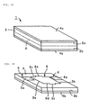
- FIGs. 1A and 1B are perspective views of a dual mode band-pass filter according to a first preferred embodiment of the present invention, showing the appearance and the structure of a resonator provided within a dielectric body, respectively.
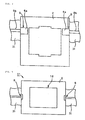
- FIG. 2 is a schematic plan view which shows the key portion of the band-pass filter.
- a dual mode band-pass filter 1 includes a dielectric body 2 that preferably has a substantially rectangular plate.
- the dielectric body 2 is preferably made of a material containing a ceramic and a glass as main constituents, capable of being fired simultaneously with Cu, Ag, or Au, having a Q value of more than about 300 at approximately 10 GHz.
- a substantially rectangular metal film 3 is preferably disposed in the dielectric body 2 at a predetermined level, as shown in FIG. 1B.
- the metal film 3 is provided to define a resonator.
- the level of the metal film 3 corresponds to the level indicated by a broken line A in FIG. 1A.
- Protrusions 3e and 3f are disposed on longer sides 3c and 3d of the metal film 3, respectively.
- the protrusions 3e and 3f are arranged to combine two resonant modes occurring in the metal film 3 which will be described below.
- Input-output coupling circuits 5 and 6 are arranged at the short sides 3a and 3b of the metal film 3, respectively, with gaps being provided therebetween.
- the input-output coupling circuits 5 and 6 include input-output capacitance-forming patterns 5a and 6a which are capacitively coupled with the metal film 3.
- the input-output capacitance-forming patterns 5a and 6a are connected to strip lines 5b and 6b as external lines through side electrodes disposed on the sides of the dielectric body 2 and via-hole electrodes disposed in the dielectric body 2.
- the strip lines 5b and 6b are arranged on a dielectric mother body 21 which is separate from the dielectric body 2.
- a ground electrode 4a is arranged substantially over the entire upper surface of the dielectric body 2, and a ground electrode 4b is arranged substantially over the entire lower surface of the dielectric body 2. That is, the ground electrodes 4a and 4b are opposed to each other with the metal film 3 and the dielectric body 2 therebetween.
- the dual mode band-pass filter 1 preferably has a triplate structure in which the ground electrodes 4a and 4b are disposed on and under the metal film 3 with the dielectric body 2 therebetween.
- the metal film 3 and the input-output coupling circuits 5 and 6 may be disposed on the upper surface of the dielectric body 2.
- the ground electrode 4a is not provided, and only the ground electrode 4b is provided. That is, the metal film 3 may be disposed either on an upper surface 2a, as the first main surface of the dielectric body 2, or in the dielectric body 2 at a predetermined level. The metal film 3 is partially formed at such a level on or in the dielectric body.
- ground electrodes 4a and 4b may be provided in the dielectric body 2.
- the dual mode band-pass filter 1 when an input voltage is applied from the input-output coupling circuits 5 and 6, in the metal film 3, a resonant mode propagating in the direction of the longer sides 3c and 3d, i.e., in the direction connecting between coupling points of the input-output coupling circuits 5 and 6 with the metal film 3, and a resonant mode propagating in a direction that is substantially perpendicular to the above propagating direction, i.e., in the extending direction of the shorter sides 3a and 3b, occur.
- the two resonant modes have different resonant frequencies
- the protrusions 3e and 3f are arranged so as to combine the two resonant modes.
- the characteristics as the dual mode band-pass filter are obtained by combining the two resonant modes occurring in the metal film 3, i.e., the resonant mode propagating in the direction connecting between the coupling points of the input-output coupling circuits 5 and 6 with the metal film 3 and the resonant mode propagating in the direction that is substantially to the above-described direction. Therefore, the shape of the metal film 3 is not limited to being substantially rectangular, and the metal film 3 of any given shape, such as a substantially rhombic metal film or a substantially elliptic metal film, may be used, thus increasing design versatility.
- the metal film 3 may be isotropic in shape, and for example, a substantially circular or a substantially square metal film may be used.
- a substantially circular or a substantially square metal film may be used.
- the other feature of the dual mode band-pass filter 1 is that the dielectric body 2 is constructed using the predetermined dielectric ceramic described above. That is, the dielectric body 2 preferably includes a dielectric ceramic containing a ceramic and a glass as main constituents, and capable of being fired simultaneously with any one of Cu, Ag, and Au. Therefore, when the metal film 3 and the input-output capacitance-forming patterns 5a and 6a preferably include Cu, Ag, or Au, it is possible to efficiently and easily form the dielectric body 2 simultaneously with the metal film 3 and the input-output capacitance-forming patterns 5a and 6a by firing using a known integrated firing technique.
- ground electrodes 4a and 4b using Cu, Ag, or Au, it is possible to form the ground electrodes 4a and 4b by baking them simultaneously with the dielectric body 2.
- the dielectric ceramic preferably has a Q value of more than approximately 300 at about 10 GHz, the dielectric loss occurring when used at a frequency band of about 10 GHz or more is low, and therefore, the insertion loss of the dual mode band-pass filter can be decreased.
- a resonator 11 including a metal film 13 which does not have protrusions As shown in FIG. 3, in the resonator 11, only a resonant mode in the direction of longer sides of a dual mode band-pass filter can be selected.
- the insertion loss (IL) of the dual mode band-pass filter is evaluated indirectly.
- the resonant frequency is a frequency of the resonant mode excited in the metal film 13
- the bandwidth is a bandwidth of the resonant mode of the resonator 11 at the point in which the amount of attenuation is decreased from the peak value by about 3 dB
- the loaded Q value is a Q value determined by both the loss of the resonator (unloaded Q) and the loss of the external circuit.
- -IL is the peak value of the resonant mode S 21 . Therefore, by measuring the resonant frequency of the resonant mode of the resonator, the bandwidth, and the insertion loss (IL), the unloaded Q can be determined.
- a resonator 11 was manufactured in which the dielectric body 2 included a dielectric ceramic having a relative dielectric constant of about 7.0 and a dielectric Q value of approximately 3,000 at about 10 GHz.
- a resonator 11 was manufactured to include a conventional BAS body with a relative dielectric constant of 6.4 and a dielectric Q value of 300 was used.
- the resonators 11 in the example and the comparative example had the same structures and sizes with respect to the individual sections.
- the resonant frequency of the resonant mode occurring in the metal film 13 was approximately 30 GHz.
- the unloaded Q value was 85
- the unloaded Q value was 235.
- the unloaded Q value was increased by about three times.
- a dual mode band-pass filter in accordance with preferred embodiments described above was manufactured in which protrusions 3e and 3f were provided so as to combine two resonant modes.
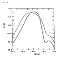
- FIG. 4 shows the frequency characteristics with respect to the dual mode band-pass filter in this example and, for comparison, a band-pass filter that was manufactured in the same manner as that of the example apart from the fact that the dielectric body was a BAS body.
- the solid line represents the results of the example and the broken line represents the results of the comparative example.
- the peak value of the resonant mode S21 is increased, and in terms of insertion loss, the band pass filter in the comparative example exhibits 2.63 dB while the dual mode band-pass filter in the example exhibits 2.08 dB, and thus it is obvious that the insertion loss is greatly decreased in preferred embodiments of the present invention.
- the protrusions 3e and 3f are provided in order to combine two resonant modes in preferred embodiments described above, instead of the protrusions 3e and 3f, openings may be provided in the metal film 3, or alternatively, cut-outs may be provided on the periphery of the metal film 3. That is, by forming the protrusions 3e and 3f, openings, cut-outs, or other similar formations, so that the resonance electric field or the resonance current during the resonance of one of two resonant modes propagating in the shorter side direction and in the longer side direction of the substantially rectangular metal film 3 is controlled, the two resonant modes can be combined. Accordingly, in the dual mode band-pass filter in preferred embodiments of the present invention, the element for combining the two resonant modes is not particularly limited, and various ways, such as protrusions, openings, and cut-outs, may be used.
- the insertion loss of the dual mode band-pass filter is effectively decreased.
- the dielectric ceramic will be described more specifically.
- the dielectric ceramic has the Q value of approximately 300 or more at about 10 GHz or more.
- Wet mixing was performed for 16 hours, followed by drying. The dried mixture was calcined at 1,400°C for 2 hours and then was pulverized.
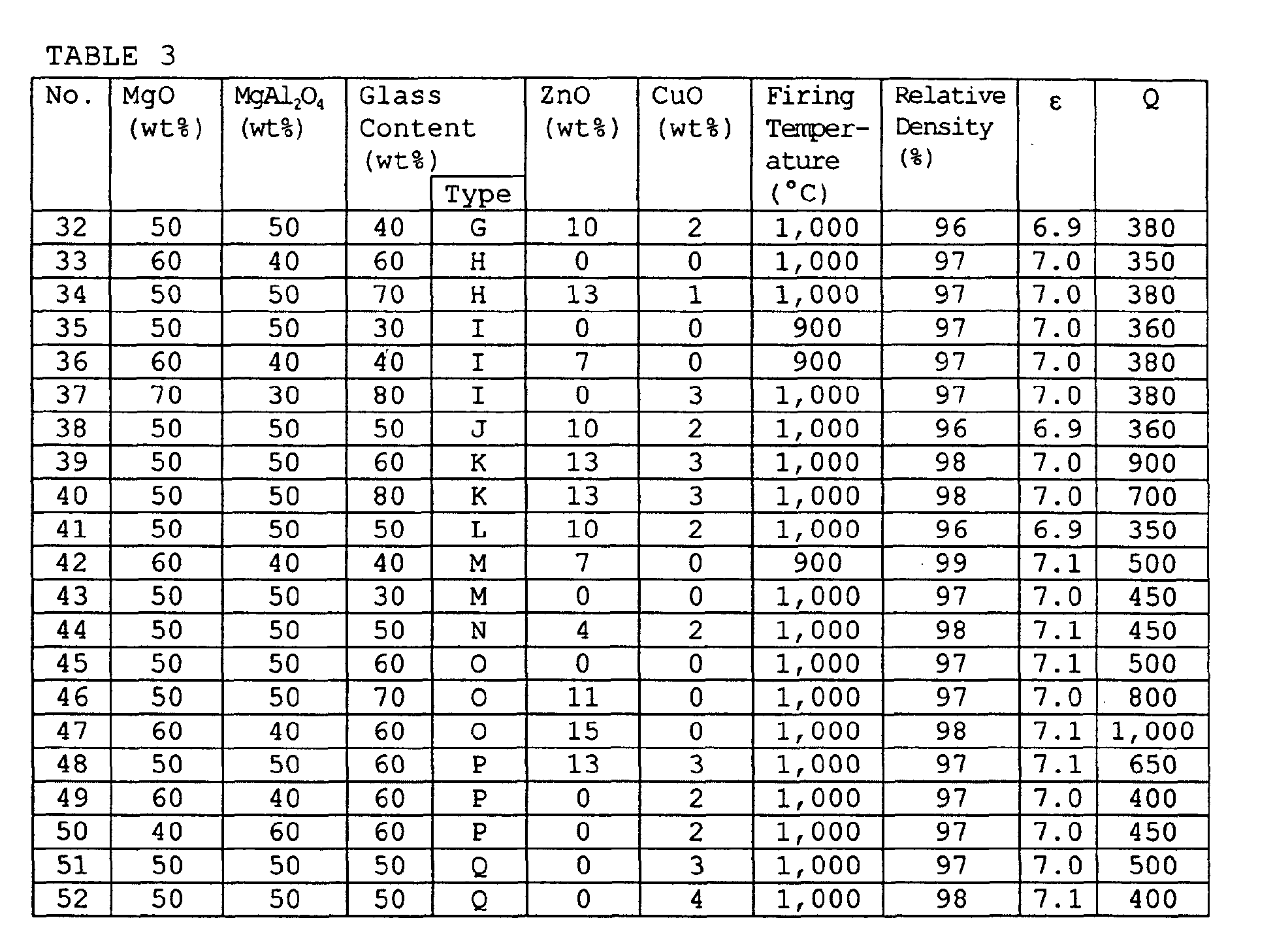
- glass powder having compositions shown in Table 1 below, approximately 20% to approximately 80% by weight of the raw material calcined as described above, and ZnO and CuO were formulated according to the ratios shown in Tables 2 and 3, an appropriate amount of binder was added thereto, and granulation was performed.
- Each of the mixtures under Nos. 1 to 52 in Tables 2 and 3 was molded at a pressure of 200 MPa to produce a columnar green compact with a diameter of about 12 mm and a thickness of about 7 mm.
- the green compacts were fired in air at 900 to 1,000°C for 2 hours, and the columnar insulating ceramics under Nos. 1 to 52 in Tables 2 and 3 were produced.
- the flexural strength was evaluated by the 3-point bending test according to JIS R1601. In the sample Nos. 2 to 7, 9 to 29, 39 to 40, and 42 to 52, the relative density was about 98% or more, and a high flexural strength of about 200 MPa was exhibited.
- any one of dielectric ceramics under Sample Nos. 1 to 52 has a higher Q value at about 10 GHz in comparison with the BAS material, and the Q value exceeds approximately 300.
- the Q value can be increased to about 400 or more, and thus it is possible to provide a dual mode band-pass filter in which the insertion loss is further decreased.
Landscapes
- Control Of Motors That Do Not Use Commutators (AREA)
Abstract
Description
| SiO2 (wt%) | B2O3 (wt%) | Al2O3 (wt%) | MgO (wt%) | BaO (wt%) | SrO (wt%) | CaO (wt%) | Li2O (wt%) | |
| A | 22 | 43 | 8 | 22 | - | - | - | 2 |
| B | 20 | 41 | 6 | 28 | - | - | - | 3 |
| | 13 | 60 | 10 | 12 | - | - | - | 5 |
| D | 50 | 25 | 3 | 17 | - | - | - | 5 |
| E | 45 | 3 | 20 | 25 | - | - | - | 7 |
| F | 42 | 13 | 5 | - | - | - | 40 | - |
| G | 12 | 60 | 10 | 13 | - | - | - | 5 |
| H | 51 | 25 | 3 | 16 | - | - | - | 5 |
| I | 13 | 61 | 10 | 11 | - | - | - | 5 |
| J | 45 | 3 | 21 | 25 | - | - | - | 6 |
| K | 33 | 33 | - | - | - | - | 24 | 10 |
| L | 45 | 2 | 20 | 25 | - | - | - | 8 |
| M | 35 | 36 | 20 | - | 5 | 4 | - | - |
| N | 19 | 40 | - | 22 | - | - | 19 | - |
| O | 23 | 52 | 6 | 17 | - | - | - | 2 |
| P | 33 | 33 | - | - | - | - | 23 | 11 |
| Q | 22 | 35 | 12 | 22 | - | - | - | 9 |

Claims (19)
- A dual mode band-pass filter (1) comprising:a dielectric body (2) having first and second main surfaces (2a and 2b);a metal film (3) partially disposed on the first main surface (2a) of the dielectric body (2) or at a certain level in the dielectric body (2), the metal film (3) having one of an opening, a protrusion (3e,3f), and a cut-out arranged to combine two resonant modes;a ground electrode (4a,4b) disposed on the second main surface (2b) or in the interior of the dielectric body (2) so as to be opposed to the metal film (3) via a portion of the dielectric body (2) therebetween; anda pair of input-output coupling circuits (5,6) being coupled with different portions (3a,3b) of the metal film (3);wherein the dielectric body (2) includes a dielectric ceramic containing a ceramic and a glass as main constituents, and is capable of being fired simultaneously with any one of Cu, Ag, and Au, and having a Q value of more than approximately 300 at about 10 GHz.
- A dual mode band-pass filter (1) according to Claim 1, further comprising a plurality of protrusions (3e,3f) disposed on longer sides (3c,3d) of the metal film (3).
- A dual mode band-pass filter (1) according to Claim 2, wherein the plurality of protrusions (3e,3f) are arranged to combine two resonant modes.
- A dual mode band-pass filter (1) according to one of Claims 1 to 3, wherein the input-output coupling circuits (5,6) are arranged at shorter sides (3a,3b) of the metal film (3).
- A dual mode band-pass filter (1) according to one of Claims 1 to 4, further comprising capacitance-forming patterns (5a,6a) capacitively coupled with the metal film (3).
- A dual mode band-pass filter (1) according to one of Claims 1 to 5, wherein the metal film (3) and the input-output coupling circuits (5,6) are disposed on the upper surface of the dielectric body (2).
- A dual mode band-pass filter (1) comprising: a dielectric body having first and second main surfaces; a metal film disposed on the first main surface of the dielectric body or at a certain level in the dielectric body, the metal film having one of at least a pair of openings, at least a pair of protrusions, and at least a pair of cut-outs arranged to combine two resonant modes; a ground electrode arranged opposite to the metal film via a portion of the dielectric body therebetween, and a pair of input-output coupling circuits being coupled with different portions of the metal film;
wherein the dielectric body includes a dielectric ceramic containing a ceramic and a glass as main constituents, and is capable of being fired simultaneously with any one of Cu, Ag, and Au, and having a Q value of more than approximately 300 at about 10 GHz. - A dual mode band-pass filter (1) according to one of Claims 1 to 7, wherein the dielectric body is made of a sintered material including a Mgo-MgAl2O4-based ceramic powder and a glass powder containing about 13% to about 50% by weight SiO2, about 3% to about 60% by weight B2O3, and about 0% to about 20% by weight Al2O3.
- A dual mode band-pass filter (1) according to Claim 8, wherein the glass powder contains at least one alkaline-earth metal oxide selected from the group consisting of BaO, SrO, CaO, and MgO in an amount of about 10% to about 40% by weight of the total glass powder.
- A dual mode band-pass filter (1) according to Claim 8 or 9, wherein the glass powder contains at least on alkali metal oxide selected from the group consisting of Li2O, K2O, and Na2O in an amount of about 10% by weight or less of the total glass powder.
- A dual mode band-pass filter (1) according to one of Claims 8 to 10, wherein the dielectric body contains about 15% by weight or less ZnO.
- A dual mode band-pass filter (1) according to one of Claims 8 to 11, wherein the dielectric body contains about 3% by weight or less CuO.
- A dual mode band-pass filter (1) according to one of Claims 8 to 12, wherein the MgO-MgAl2O4, where x and y satisfy the relationship 10 ≤ x ≤ 90 and 10 ≤ y ≤ 90, respectively, and x + y = 100.
- A dual mode band-pass filter (1) according to one of Claims 8 to 13,
wherein the weight ratio of the ceramic powder to the glass powder is approximately 20:80 to approximately 80:20. - A dual mode band-pass filter (1) according to one of Claims 1 to 14, wherein the dielectric body is substantially rectangular.
- A dual mode band-pass filter (1) according to one of Claims 1 to 15, wherein the dual mode band-pass filter (1) has a triplate structure in which ground electrodes (4a,4b) are disposed on and under the metal film (3) with the dielectric body (2) disposed therebetween.
- A dual mode band-pass filter (1) according to one of Claims 1 to 17, wherein the metal film (3) has a shape that is one of substantially rectangular, substantially rhombic, substantially elliptic, substantially circular and substantially square.
- A dual mode band-pass filter (1) according to Claim 2, wherein the glass powder contains at least one alkaline-earth metal oxide selected from the group consisting of BaO, SrO, CaO, and MgO in an amount of about 10% to about 40% by weight of the total glass powder.
- A dual mode band-pass filter (1) according to Claim 18, wherein the dielectric body contains about 3% by weight or less CuO.
Applications Claiming Priority (2)
| Application Number | Priority Date | Filing Date | Title |
|---|---|---|---|
| JP2000158658A JP2001339203A (en) | 2000-05-29 | 2000-05-29 | Dual-mode band-pass filter |
| JP2000158658 | 2000-05-29 |
Publications (3)
| Publication Number | Publication Date |
|---|---|
| EP1160909A2 true EP1160909A2 (en) | 2001-12-05 |
| EP1160909A3 EP1160909A3 (en) | 2003-05-07 |
| EP1160909B1 EP1160909B1 (en) | 2009-03-25 |
Family
ID=18663092
Family Applications (1)
| Application Number | Title | Priority Date | Filing Date |
|---|---|---|---|
| EP01111070A Expired - Lifetime EP1160909B1 (en) | 2000-05-29 | 2001-05-08 | Dual mode band-pass filter |
Country Status (4)
| Country | Link |
|---|---|
| US (1) | US6563403B2 (en) |
| EP (1) | EP1160909B1 (en) |
| JP (1) | JP2001339203A (en) |
| DE (1) | DE60138067D1 (en) |
Cited By (2)
| Publication number | Priority date | Publication date | Assignee | Title |
|---|---|---|---|---|
| CN105489979A (en) * | 2014-09-20 | 2016-04-13 | 南京理工大学 | Multimode resonator-based tri-bandpass filter |
| CN111463527A (en) * | 2020-03-05 | 2020-07-28 | 东北大学秦皇岛分校 | Dual-band bandpass filter and design method based on unequal length cross resonator |
Families Citing this family (11)
| Publication number | Priority date | Publication date | Assignee | Title |
|---|---|---|---|---|
| US6825740B2 (en) * | 2002-02-08 | 2004-11-30 | Tdk Corporation | TEM dual-mode rectangular dielectric waveguide bandpass filter |
| US6825742B1 (en) | 2002-12-30 | 2004-11-30 | Raytheon Company | Apparatus and methods for split-feed coupled-ring resonator-pair elliptic-function filters |
| JP2004297764A (en) * | 2003-03-07 | 2004-10-21 | Murata Mfg Co Ltd | Bandpass filter |
| JP2004304761A (en) * | 2003-03-18 | 2004-10-28 | Murata Mfg Co Ltd | Chip type resonance parts |
| JP4066931B2 (en) * | 2003-11-06 | 2008-03-26 | 大同特殊鋼株式会社 | Method of manufacturing bandpass filter for GHz band |
| EP1909354A1 (en) * | 2006-10-05 | 2008-04-09 | Fujikura Ltd. | Reflection-type bandpass filter |
| JP2008098701A (en) * | 2006-10-05 | 2008-04-24 | Fujikura Ltd | Reflective bandpass filter |
| JP2008098702A (en) * | 2006-10-05 | 2008-04-24 | Fujikura Ltd | Reflective bandpass filter |
| EP1909352B1 (en) * | 2006-10-05 | 2013-05-15 | Fujikura Ltd. | Reflection-type bandpass filter |
| JP2008098705A (en) * | 2006-10-05 | 2008-04-24 | Fujikura Ltd | Reflective bandpass filter |
| CN103943935B (en) * | 2014-04-18 | 2016-09-28 | 苏州金牛精密机械有限公司 | A kind of radio-frequency filter printing fixture |
Family Cites Families (15)
| Publication number | Priority date | Publication date | Assignee | Title |
|---|---|---|---|---|
| US5136268A (en) * | 1991-04-19 | 1992-08-04 | Space Systems/Loral, Inc. | Miniature dual mode planar filters |
| US5172084A (en) * | 1991-12-18 | 1992-12-15 | Space Systems/Loral, Inc. | Miniature planar filters based on dual mode resonators of circular symmetry |
| JP2906863B2 (en) | 1992-09-28 | 1999-06-21 | 松下電器産業株式会社 | Stripline dual mode filter |
| US5805034A (en) * | 1995-03-17 | 1998-09-08 | Lucent Technologies Inc. | Microstrip patch filters |
| JP3304724B2 (en) | 1995-11-16 | 2002-07-22 | 松下電器産業株式会社 | Dual mode filter |
| JPH09162610A (en) | 1995-12-14 | 1997-06-20 | Matsushita Electric Ind Co Ltd | Dual mode resonator |
| KR100203515B1 (en) * | 1996-06-11 | 1999-06-15 | 김병규 | Ceramic dielectric composition for high frequency |
| US5939958A (en) * | 1997-02-18 | 1999-08-17 | The United States Of America As Represented By The Secretary Of The Navy | Microstrip dual mode elliptic filter with modal coupling through patch spacing |
| JPH10330165A (en) * | 1997-05-30 | 1998-12-15 | Kyocera Corp | High frequency dielectric porcelain |
| JPH11228222A (en) * | 1997-12-11 | 1999-08-24 | Murata Mfg Co Ltd | Dielectric ceramic composition and ceramic electronic part using the same |
| JPH11310455A (en) * | 1998-02-27 | 1999-11-09 | Murata Mfg Co Ltd | Dielectric porcelain composition and ceramic electronic part using the same |
| US6258462B1 (en) * | 1998-04-13 | 2001-07-10 | Matsushita Electric Industrial Co., Ltd. | Dielectric ceramic composition and device for communication apparatus using the same |
| JP3860336B2 (en) * | 1998-04-28 | 2006-12-20 | 日本特殊陶業株式会社 | Glass ceramic composite |
| US6348424B1 (en) * | 1998-11-11 | 2002-02-19 | Nec Corporation | Low-temperature calcined glass ceramic and a manufacturing process therefor |
| JP3680684B2 (en) * | 2000-03-06 | 2005-08-10 | 株式会社村田製作所 | Insulator porcelain, ceramic multilayer substrate, ceramic electronic component and multilayer ceramic electronic component |
-
2000
- 2000-05-29 JP JP2000158658A patent/JP2001339203A/en active Pending
-
2001
- 2001-05-08 EP EP01111070A patent/EP1160909B1/en not_active Expired - Lifetime
- 2001-05-08 DE DE60138067T patent/DE60138067D1/en not_active Expired - Lifetime
- 2001-05-29 US US09/867,250 patent/US6563403B2/en not_active Expired - Fee Related
Cited By (3)
| Publication number | Priority date | Publication date | Assignee | Title |
|---|---|---|---|---|
| CN105489979A (en) * | 2014-09-20 | 2016-04-13 | 南京理工大学 | Multimode resonator-based tri-bandpass filter |
| CN105489979B (en) * | 2014-09-20 | 2018-07-31 | 南京理工大学 | Three band-pass filters based on multimode resonator |
| CN111463527A (en) * | 2020-03-05 | 2020-07-28 | 东北大学秦皇岛分校 | Dual-band bandpass filter and design method based on unequal length cross resonator |
Also Published As
| Publication number | Publication date |
|---|---|
| US20020053960A1 (en) | 2002-05-09 |
| DE60138067D1 (en) | 2009-05-07 |
| EP1160909A3 (en) | 2003-05-07 |
| EP1160909B1 (en) | 2009-03-25 |
| US6563403B2 (en) | 2003-05-13 |
| JP2001339203A (en) | 2001-12-07 |
Similar Documents
| Publication | Publication Date | Title |
|---|---|---|
| KR100434422B1 (en) | High frequency ceramic compact, use thereof and method of producing the same | |
| US6563403B2 (en) | Dual mode band-pass filter | |
| EP1043288B1 (en) | High-frequency dielectric ceramic composition, dielectric resonator, dielectric filter, dielectric duplexer, and communication apparatus | |
| EP1170269A2 (en) | High frequency dielectric ceramic compact, dielectric resonator, dielectric filter, dielectric duplexer, and communication apparatus | |
| KR100521278B1 (en) | High-frequency dielectric ceramic member, dielectric resonator, dielectric filter, dielectric duplexer, and communication device | |
| KR100406123B1 (en) | High Frequency Dielectric Ceramic Composition, Dielectric Resonator, Dielectric Filter, Dielectric Duplexer, and Communication System | |
| EP1172345B1 (en) | Dielectric ceramic for high frequency, dielectric resonator, dielectric filter, dielectric duplexer and communication unit | |
| JPH05275903A (en) | Lamination type dielectric filter | |
| JP4839496B2 (en) | High frequency dielectric ceramic composition, dielectric resonator, dielectric filter, dielectric duplexer, and communication device | |
| US6844284B2 (en) | Dielectric porcelain composition | |
| JP4513076B2 (en) | High frequency dielectric ceramic composition, dielectric resonator, dielectric filter, dielectric duplexer, and communication device | |
| US6940371B2 (en) | High frequency dielectric ceramic composition, dielectric resonator, dielectric filter, dielectric duplexer, and communication device | |
| JPH05152804A (en) | Dielectric filter and adjustment method of its frequency characteristic | |
| JP3454535B2 (en) | Multilayer dielectric filter | |
| JP3376933B2 (en) | High frequency dielectric ceramic composition and dielectric resonator | |
| JP3979433B2 (en) | High frequency dielectric ceramic composition, dielectric resonator, dielectric filter, dielectric duplexer, and communication device | |
| JP4493225B2 (en) | Multilayer dielectric filter | |
| JP4895417B2 (en) | High frequency electronic substrate | |
| JP2001285024A (en) | High frequency filter | |
| JP3575336B2 (en) | High frequency dielectric ceramic composition, dielectric resonator, dielectric filter, dielectric duplexer, and communication device | |
| JP2004051385A (en) | Dielectric porcelain composition and dielectric resonator | |
| JPH1146048A (en) | High frequency wiring board | |
| JP2002145668A (en) | Dielectric ceramic composition for high frequency wave, dielectric resonator, dielectric filter, dielectric duplexer and communication equipment | |
| JP2004123466A (en) | Dielectric porcelain for high-frequency use, dielectric resonator, dielectric filter, dielectric duplexer and communication instrument | |
| JPH1149563A (en) | High frequency wiring board |
Legal Events
| Date | Code | Title | Description |
|---|---|---|---|
| PUAI | Public reference made under article 153(3) epc to a published international application that has entered the european phase |
Free format text: ORIGINAL CODE: 0009012 |
|
| 17P | Request for examination filed |
Effective date: 20010508 |
|
| AK | Designated contracting states |
Kind code of ref document: A2 Designated state(s): AT BE CH CY DE DK ES FI FR GB GR IE IT LI LU MC NL PT SE TR |
|
| AX | Request for extension of the european patent |
Free format text: AL;LT;LV;MK;RO;SI |
|
| PUAL | Search report despatched |
Free format text: ORIGINAL CODE: 0009013 |
|
| AK | Designated contracting states |
Designated state(s): AT BE CH CY DE DK ES FI FR GB GR IE IT LI LU MC NL PT SE TR |
|
| AX | Request for extension of the european patent |
Extension state: AL LT LV MK RO SI |
|
| AKX | Designation fees paid |
Designated state(s): DE FR GB |
|
| RAP1 | Party data changed (applicant data changed or rights of an application transferred) |
Owner name: MURATA MANUFACTURING CO., LTD. |
|
| 17Q | First examination report despatched |
Effective date: 20071011 |
|
| GRAP | Despatch of communication of intention to grant a patent |
Free format text: ORIGINAL CODE: EPIDOSNIGR1 |
|
| GRAS | Grant fee paid |
Free format text: ORIGINAL CODE: EPIDOSNIGR3 |
|
| GRAA | (expected) grant |
Free format text: ORIGINAL CODE: 0009210 |
|
| AK | Designated contracting states |
Kind code of ref document: B1 Designated state(s): DE FR GB |
|
| REG | Reference to a national code |
Ref country code: GB Ref legal event code: FG4D |
|
| REF | Corresponds to: |
Ref document number: 60138067 Country of ref document: DE Date of ref document: 20090507 Kind code of ref document: P |
|
| PLBE | No opposition filed within time limit |
Free format text: ORIGINAL CODE: 0009261 |
|
| STAA | Information on the status of an ep patent application or granted ep patent |
Free format text: STATUS: NO OPPOSITION FILED WITHIN TIME LIMIT |
|
| GBPC | Gb: european patent ceased through non-payment of renewal fee |
Effective date: 20090625 |
|
| REG | Reference to a national code |
Ref country code: FR Ref legal event code: ST Effective date: 20100129 |
|
| 26N | No opposition filed |
Effective date: 20091229 |
|
| PG25 | Lapsed in a contracting state [announced via postgrant information from national office to epo] |
Ref country code: FR Free format text: LAPSE BECAUSE OF NON-PAYMENT OF DUE FEES Effective date: 20090602 |
|
| PG25 | Lapsed in a contracting state [announced via postgrant information from national office to epo] |
Ref country code: GB Free format text: LAPSE BECAUSE OF NON-PAYMENT OF DUE FEES Effective date: 20090625 |
|
| PGFP | Annual fee paid to national office [announced via postgrant information from national office to epo] |
Ref country code: DE Payment date: 20200520 Year of fee payment: 20 |
|
| REG | Reference to a national code |
Ref country code: DE Ref legal event code: R071 Ref document number: 60138067 Country of ref document: DE |