EP1160866A2 - Power wiring structure and semiconductor device - Google Patents
Power wiring structure and semiconductor device Download PDFInfo
- Publication number
- EP1160866A2 EP1160866A2 EP01112178A EP01112178A EP1160866A2 EP 1160866 A2 EP1160866 A2 EP 1160866A2 EP 01112178 A EP01112178 A EP 01112178A EP 01112178 A EP01112178 A EP 01112178A EP 1160866 A2 EP1160866 A2 EP 1160866A2
- Authority
- EP
- European Patent Office
- Prior art keywords
- power
- line
- wiring structure
- power line
- semiconductor device
- Prior art date
- Legal status (The legal status is an assumption and is not a legal conclusion. Google has not performed a legal analysis and makes no representation as to the accuracy of the status listed.)
- Granted
Links
Images





Classifications
-
- H—ELECTRICITY
- H10—SEMICONDUCTOR DEVICES; ELECTRIC SOLID-STATE DEVICES NOT OTHERWISE PROVIDED FOR
- H10W—GENERIC PACKAGES, INTERCONNECTIONS, CONNECTORS OR OTHER CONSTRUCTIONAL DETAILS OF DEVICES COVERED BY CLASS H10
- H10W72/00—Interconnections or connectors in packages
-
- H—ELECTRICITY
- H10—SEMICONDUCTOR DEVICES; ELECTRIC SOLID-STATE DEVICES NOT OTHERWISE PROVIDED FOR
- H10W—GENERIC PACKAGES, INTERCONNECTIONS, CONNECTORS OR OTHER CONSTRUCTIONAL DETAILS OF DEVICES COVERED BY CLASS H10
- H10W44/00—Electrical arrangements for controlling or matching impedance
- H10W44/501—Inductive arrangements
-
- H—ELECTRICITY
- H10—SEMICONDUCTOR DEVICES; ELECTRIC SOLID-STATE DEVICES NOT OTHERWISE PROVIDED FOR
- H10W—GENERIC PACKAGES, INTERCONNECTIONS, CONNECTORS OR OTHER CONSTRUCTIONAL DETAILS OF DEVICES COVERED BY CLASS H10
- H10W70/00—Package substrates; Interposers; Redistribution layers [RDL]
- H10W70/60—Insulating or insulated package substrates; Interposers; Redistribution layers
- H10W70/62—Insulating or insulated package substrates; Interposers; Redistribution layers characterised by their interconnections
- H10W70/65—Shapes or dispositions of interconnections
- H10W70/658—Shapes or dispositions of interconnections for devices provided for in groups H10D8/00 - H10D48/00
-
- H—ELECTRICITY
- H10—SEMICONDUCTOR DEVICES; ELECTRIC SOLID-STATE DEVICES NOT OTHERWISE PROVIDED FOR
- H10W—GENERIC PACKAGES, INTERCONNECTIONS, CONNECTORS OR OTHER CONSTRUCTIONAL DETAILS OF DEVICES COVERED BY CLASS H10
- H10W90/00—Package configurations
-
- H—ELECTRICITY
- H10—SEMICONDUCTOR DEVICES; ELECTRIC SOLID-STATE DEVICES NOT OTHERWISE PROVIDED FOR
- H10W—GENERIC PACKAGES, INTERCONNECTIONS, CONNECTORS OR OTHER CONSTRUCTIONAL DETAILS OF DEVICES COVERED BY CLASS H10
- H10W44/00—Electrical arrangements for controlling or matching impedance
- H10W44/20—Electrical arrangements for controlling or matching impedance at high-frequency [HF] or radio frequency [RF]
- H10W44/203—Electrical connections
- H10W44/206—Wires
-
- H—ELECTRICITY
- H10—SEMICONDUCTOR DEVICES; ELECTRIC SOLID-STATE DEVICES NOT OTHERWISE PROVIDED FOR
- H10W—GENERIC PACKAGES, INTERCONNECTIONS, CONNECTORS OR OTHER CONSTRUCTIONAL DETAILS OF DEVICES COVERED BY CLASS H10
- H10W72/00—Interconnections or connectors in packages
- H10W72/071—Connecting or disconnecting
- H10W72/075—Connecting or disconnecting of bond wires
- H10W72/07551—Connecting or disconnecting of bond wires characterised by changes in properties of the bond wires during the connecting
- H10W72/07554—Connecting or disconnecting of bond wires characterised by changes in properties of the bond wires during the connecting changes in dispositions
-
- H—ELECTRICITY
- H10—SEMICONDUCTOR DEVICES; ELECTRIC SOLID-STATE DEVICES NOT OTHERWISE PROVIDED FOR
- H10W—GENERIC PACKAGES, INTERCONNECTIONS, CONNECTORS OR OTHER CONSTRUCTIONAL DETAILS OF DEVICES COVERED BY CLASS H10
- H10W72/00—Interconnections or connectors in packages
- H10W72/50—Bond wires
- H10W72/541—Dispositions of bond wires
- H10W72/547—Dispositions of multiple bond wires
-
- H—ELECTRICITY
- H10—SEMICONDUCTOR DEVICES; ELECTRIC SOLID-STATE DEVICES NOT OTHERWISE PROVIDED FOR
- H10W—GENERIC PACKAGES, INTERCONNECTIONS, CONNECTORS OR OTHER CONSTRUCTIONAL DETAILS OF DEVICES COVERED BY CLASS H10
- H10W72/00—Interconnections or connectors in packages
- H10W72/851—Dispositions of multiple connectors or interconnections
- H10W72/874—On different surfaces
- H10W72/884—Die-attach connectors and bond wires
-
- H—ELECTRICITY
- H10—SEMICONDUCTOR DEVICES; ELECTRIC SOLID-STATE DEVICES NOT OTHERWISE PROVIDED FOR
- H10W—GENERIC PACKAGES, INTERCONNECTIONS, CONNECTORS OR OTHER CONSTRUCTIONAL DETAILS OF DEVICES COVERED BY CLASS H10
- H10W90/00—Package configurations
- H10W90/20—Configurations of stacked chips
- H10W90/24—Configurations of stacked chips at least one of the stacked chips being laterally offset from a neighbouring stacked chip, e.g. chip stacks having a staircase shape
-
- H—ELECTRICITY
- H10—SEMICONDUCTOR DEVICES; ELECTRIC SOLID-STATE DEVICES NOT OTHERWISE PROVIDED FOR
- H10W—GENERIC PACKAGES, INTERCONNECTIONS, CONNECTORS OR OTHER CONSTRUCTIONAL DETAILS OF DEVICES COVERED BY CLASS H10
- H10W90/00—Package configurations
- H10W90/701—Package configurations characterised by the relative positions of pads or connectors relative to package parts
- H10W90/731—Package configurations characterised by the relative positions of pads or connectors relative to package parts of die-attach connectors
- H10W90/732—Package configurations characterised by the relative positions of pads or connectors relative to package parts of die-attach connectors between stacked chips
Definitions
- the present invention relates to a low-inductance wiring structure with semiconductor switching elements, applicable to a power inverter.
- Japanese Unexamined Patent Publication No. 6-38507 discloses a technique of layering a high-potential power bus P and a low-potential power bus N to form a two-layer electrode structure capable of reducing inductance.
- the two-layer electrode structure involving power buses P and N is applicable to an inverter module having an integrated inverter circuit, to reduce inductance. In practice, however, the two-layer structure does not always pass opposite currents of the same value because the buses P and N in the two-layer structure must supply a current to load through an output line U. In a real inverter module, a current forms a loop as shown in Fig. 1.
- the inverter module 1 of Fig. 1 involves two phases U and V. In each of U- and V-phase circuits, buses P and N are arranged to face each other with an insulator interposing between them.
- This configuration forms a current path indicated with a thick black lines and a looped current path indicated with a large dotted arrow mark depicted by C.
- opposite currents to cancel magnetic fields flow only in dotted circle areas A and B outside the inverter module 1.
- magnetic fields do not cancel each other. Consequently, the example of Fig. 1 is insufficient to provide the effect of reducing wiring inductance.
- An object of the present invention is to provide a power wiring structure of low inductance.
- Another object of the present invention is to provide a semiconductor device employing such a power wiring structure.
- an aspect of the present invention provides a power wiring structure employing two switching elements connected in series and complementarily turned on and off, power lines extending from a power source to one ends of the switching elements, and an output line extending from a node between the switching elements to load.
- the power lines include a high-potential power line P and a low-potential power line N.
- the output line is an output line U.
- the lines P, N, and U are each a wide electrode with the width thereof being greater than the thickness thereof. These lines are layered one upon another in order of P, U, and N with an insulator interposed between adjacent ones of the layered lines, to form a three-layer wide electrode structure.
- the two switching elements that are connected in series and are complementarily turned on and off correspond to, for example, an inverter circuit, an H-bridge circuit employing two inverters connected in parallel with each other, and a three-phase inverter circuit employing three inverter circuits connected in parallel with one another.
- Another aspect of the present invention employs the three-layer wide electrode structure mentioned above and arranges wiring such as bonding wires in an inverter module in such a way as to cancel magnetic fields generated by currents flowing through the wiring, thereby effectively reducing the inductance of the wiring in the inverter module.
- the wiring structures are capable of effectively reducing wiring inductance. Even at high-speed switching, the wiring structures cause no surge voltage that may break switching elements. The wiring structures, therefore, need no snubber, to thereby reduce the size and cost of apparatuses to which the wiring structures are applied.
- the wiring structures ensure high-speed switching, suppress switching loss, minimize the heating of elements, and improve efficiency.
- the wiring structures When applied to the internal wiring of inverter modules, the wiring structures effectively reduce the inductance of the internal wiring.
- Figures 2A to 2C show a power wiring structure according to an embodiment of the present invention, in which Fig. 2A is a circuit diagram, Fig. 2B a perspective view, and Fig. 2C a view showing connections in the wiring structure.
- the wiring structure is applied to a single-phase inverter containing two switching elements connected in series.
- the wiring structure covers the inverter module 1, load 2, a power source 3, the switching elements 4 and 5, and smoothing capacitors 6 and 7.
- the switching elements 4 and 5 are transistors.
- the switching elements may be thyristors , or any other switching devices .
- Each of the switching elements 4 and 5 is connected to a free wheeling diode in parallel.
- wires for connecting the components 2 to 7 are depicted with inductance symbols (coils).
- the wires include a high-potential bus P, a low-potential bus N, and an output line U.
- the buses P and N and line U are layered one upon another in order of P, U, and N, to form a three-layer structure wherein each interlayer is interposed by a thin insulator layer G.
- Each of the lines P, N, and U is a wide electrode with the width thereof being greater than the thickness thereof . Namely, the thickness d and width W of each electrode layer have the relationship of d/W ⁇ 1. Between adjacent ones of the layers, an insulator G is interposed.
- the embodiment maintains the multilayer structure as close to connections or terminals of the structure as possible, as shown in Fig. 2C.
- the switching elements 4 and 5 are oppositely turned on and off. For example, if the switching element 4 is ON, the switching element 5 is OFF. If the switching element 4 is ON, a current flows through a path indicated with a thick black line in Fig. 2A that routes through a positive terminal of the power source 3, the switching element 4, the load 2, the smoothing capacitor 7, and a negative terminal of the power source 3 in this order. In each of dotted circle areas A, B, C, D on the current path, the multilayer structure of the embodiment passes opposite currents to cancel magnetic fields produced around the electrode layers.
- the switching element 4 If the switching element 4 is OFF, the switching element 5 is ON to pass a current through a path routing through the positive terminal of the power source 3, the smoothing capacitor 6, the load 2, the switching element 5, and the negative terminal of the power source 3.
- the multilayer structure along the current path passes opposite currents to cancel magnetic fields generated around the electrode layers. This arrangement greatly reduces inductance as well as electromagnetic waves.
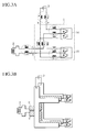
- Figures 3A and 3B show a power wiring structure for an inverter module with U- and V-phases according to another embodiment of the present invention, in which Fig. 3A is a circuit diagram and Fig. 3B a view showing connections in the wiring structure.
- the inverter module 1 has switching blocks 14 and 15 each including two switching elements each containing a transistor and a diode connected in parallel with each other.
- U- and V-phase lines are wide electrodes sandwiched between buses P and N that are also wide electrodes.
- the embodiment of Fig. 3A passes opposite currents through each part of the wiring structure, to cancel magnetic fields, thereby greatly reducing inductance.
- the number of electrode layers in the wiring structure may be three or more.
- the above embodiment connects single-phase inverters each employing the three-layer wide electrode structure in parallel with one another to form a multilayer inverter module.
- the present invention is also applicable to internal electrodes directly connected to switching elements. In this case, electrodes are formed into the multilayer wide electrode structure of Fig. 2B phase by phase, to reduce inductance and electromagnetic waves.
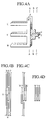
- Figures 4A-4D shows a power wiring structure according to still another embodiment of the present invention, in which Fig. 4A is a perspective view, Fig. 4B a sectional view taken along a line A-A of Fig. 4A, Fig. 4C a sectional view taken along a line B-B of Fig. 4A, and Fig. 4D a sectional view taken along a line C-C of Fig. 4A.
- This embodiment relates to, in particular, output leads of the wiring structure.
- Figs. 4A-4D The wiring structure of Figs. 4A-4D is applicable to an inverter with U-, V-, and W-phases.
- U- , V-, and W-phase output lines are each sandwiched between power buses P and N with an insulator layer being interposed between the adjacent bus and output line.
- the U-, V-, and W-phase output lines are arranged side by side.
- the U- and W-phase output lines are bent and gathered on and under the V-phase output line.
- Fig. 4D the U-, V-, and W-phase output lines are laid one upon another to form output leads.
- the thickness of the three-layer wide electrode structure is substantially equal to the thickness of three electrode plates, where the thickness also includes that of the interposed thin insulator layers.
- This three-layer structure is simple and is easy to fabricate.
- the U- , V- , and W-phase output lines stacked one upon another as shown in Figs. 4C and 4D are insulated from one another.
- Fig. 5A is a perspective view
- Fig. 5B a sectional view taken along a line A-A of Fig. 5A
- Fig. 5C a sectional view taken along a line B-B of Fig. 5A.
- Fig. 5B U- and W-phase output lines on each side of a V-phase output line are laid on and under the V-phase output line between buses P and N with an insulating layer being interposed between adjacent ones of the lines.
- the layered U-, V-, and W-phase output lines are taken out from between the buses P and N.
- This configuration forms no discrete output line, and therefore, surely reduces the inductance of the output lines.
- this arrangement stacks the U-, V-, and W-phase output lines one upon another between the buses P and N, to pass opposing currents between the buses P and N and the output lines at a position where the output lines are taken out from between the buses P and N, thereby effectively reducing the inductance of the buses P and N at the position.
- FIG. 6A is a perspective view
- Fig. 6B a circuit diagram. This embodiment corresponds to the single-phase inverter embodiment of Fig. 2.
- an insulating substrate 20, a switching transistor 21, a free wheeling diode 22, and a conductive film 23 for connecting a signal line for the gate of the transistor 21 form a switching element (corresponding to the switching element 4 of Fig. 2A) on an upper arm.
- an insulating substrate 24, a transistor 25, a free wheeling diode 26, and a conductive film 27 form a switching element (corresponding to the switching element 5 of Fig. 2A) on a lower arm.
- the switching elements on the upper and lower arms are arranged on each side of a three-layer wide electrode structure 29.
- the transistors 21 and 25 and free wheeling diodes 22 and 26 are formed on conductive films 28, respectively, with bottom electrodes of these elements 21, 25, 22, and 26 connected to the conductive films , respectively.
- Top electrodes of the elements 21, 25, 22 and 26 are connected to the electrode structure 29 through bonding wires 30.
- the conductive films 28 are connected to the electrode structure 29 through bonding wires 30.
- the high-potential side i.e. the bottom electrode of the upper arm is connected to an electrode P of the electrode structure 29 through the bonding wires
- the low-potential side i.e. the top electrode of the upper arm is connected to an electrode U of the electrode structure 29
- the high-potential side of the lower arm is connected to the electrode U
- the low-potential side of the lower arm is connected to an electrode N of the electrode structure 29.
- the conductive films for the transistor and free wheeling diode on each insulating substrate (20, 24) must be separated from each other and must separately be connected to the electrode structure 29 through bonding wires.
- the transistor 21 and free wheeling diode 22 of the upper arm face the free wheeling diode 26 and transistor 25 of the lower arm with the electrode structure 29 interposing between them.
- Input and output currents flowing through the transistors and free wheeling diodes are oppositely oriented to reduce inductance.
- the transistors and free wheeling diodes of the upper and lower arms are opposed to each other, so that, as soon as one transistor turns off, transient induced current circulates through the opposite free wheeling diode. This arrangement shortens wire lengths to reduce inductance.
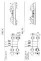
- Figures 7A to 7D show current flows during the operation of the inverter module of Figs. 6A and 6B.
- a left half is a circuit diagram and a right half a sectional view.
- Figure 7A shows a state that the transistor 21 of the upper arm is ON
- Fig. 7B a state that the transistor 21 is OFF to pass transient induced current through the free wheeling diode 26 of the lower arm
- Fig. 7C a state that the transistor 25 of the lower arm is ON
- Fig. 7D a state that the transistor 25 is OFF to pass transient current through the free wheeling diode 22 of the upper arm.
- Figures 8A and 8B are sectional views showing different arrangements of the transistors and free wheeling diodes of the inverter module of Fig. 6A.
- the free wheeling diodes 22 and 26 are arranged close to the three-layer wide electrode structure 29 on each side of the electrode structure 29, and the transistors 21 and 25 are arranged on the outer sides of the free wheeling diodes 22 and 26, respectively.
- the free wheeling diodes and transistors are arranged on each side of the electrode structure 29 along a line that is orthogonal to the longitudinal axis of the electrode structure 29.
- a metal film 32 on an insulating substrate 31 serves for both the transistor 21 and free wheeling diode 22, and a metal film 33 on the insulating substrate 31 serves for both the transistor 25 and free wheeling diode 26, to share bonding wires to the electrode structure 29.
- the transistors and free wheeling diodes on the upper and lower arms face each other, to reduce inductance like the embodiment of Figs. 6A and 6B.
- the three-layer wide electrode structure 29 is inclined to equalize the heights of connection points between the upper and lower arms. This arrangement equalizes wiring lengths between the upper and lower arms to equalize inductance between them. This equalizes surge voltages between the upper and lower arms and balances electric characteristics between them.
- the transistors and free wheeling diodes are roughly depicted. They may be arranged like Fig. 8A or Fig. 6A.
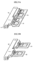
- Figures 9A and 9B are perspective views showing other arrangements of the upper and lower arms of Fig. 6A.
- the upper and lower arms are arranged side by side on one side of the three-layer wide electrode structure 29.
- the transistors and free wheeling diodes are arranged substantially in parallel with the length of the electrode structure 29, like Fig. 6A.
- the free wheeling diodes and transistors are arranged along lines that are orthogonal to the length of the electrode structure 29, like Fig. 8A.
- Figs. 9A and 9B collectively arrange the semiconductor elements, to make the fabrication thereof easier.
- the embodiment of Fig. 9A shortens transistor wiring, to reduce inductance.
- the embodiment of Fig. 9B shares bonding wires for conductive films on each substrate, to make the fabrication of the inverter module easier.
- any one of the embodiments may employ a common insulating substrate for upper and lower arms.
Landscapes
- Inverter Devices (AREA)
- Power Conversion In General (AREA)
- Semiconductor Integrated Circuits (AREA)
Abstract
Description
Claims (11)
- A power wiring structure comprising a circuit containing a first power line, a second power line, and an output line to load, the first power line being connected to a high-potential power source, the second power line being connected to a low-potential power source, the circuit being connected to first and second switching elements that are connected in series and are complementarily turned on and off, a node between the first and second switching elements being connected to the output line, wherein:the first power line, second power line, and output line are each a wide electrode with the width thereof greater than the thickness thereof; andthe first power line, second power line, and output line are layered one upon another in a thickness direction in order of the first power line, output line, and second power line with an insulator interposed between adjacent ones of the layered lines.
- The power wiring structure of claim 1, wherein:
the output line includes a plurality of lines of different phases, output ends of these lines being collected and layered one upon another between the first and second power lines. - A semiconductor device comprising:a power wiring structure including a first power line, a second power line, and an output line, these lines being each a wide electrode with the width thereof greater than the thickness thereof and being layered one upon another in order of the first power line, output line, and second power line with an insulator interposed between adjacent ones of the layered lines;a first conductive layer selectively formed on a first insulating substrate;a first semiconductor chip formed on the first conductive layer; having a bottom electrode electrically connected to the first conductive layer;a second conductive layer selectively formed on a second insulating substrate;a second semiconductor chip formed on the second conductive layer, having a bottom electrode electrically connected to the second conductive layer;means for electrically connecting the first conductive layer to the first power line;means for electrically connecting a top electrode of the first semiconductor chip to the output line;means for electrically connecting a top electrode of the second semiconductor chip to the second power line; andmeans for electrically connecting the second conductive layer to the output line.
- The semiconductor device of claim 3, wherein:
the first and second insulating substrates are arranged on each side of the power wiring structure. - The semiconductor device of claim 3, wherein:the first and second insulating substrates are arranged on each side of the power wiring structure; andthe power wiring structure is inclined to substantially equalize the heights of wiring connection points between the first and second insulating substrates.
- The semiconductor device of claim 3, wherein:
the first and second insulating substrates are arranged side by side on one side of the power wiring structure along the length of the power wiring structure. - The semiconductor device of any one of claims 3 to 6, wherein:each of the semiconductor chips includes a switching element and a free wheeling diode;the switching element and free wheeling diode are arranged side by side along the length of the power wiring structure; andthe conductive layer for each semiconductor chip is separated into two, one for a bottom electrode of the switching element and another for a bottom electrode of the free wheeling diode.
- The semiconductor device of any one of claims 3 to 6, wherein:each of the semiconductor chips includes a switching element and a free wheeling diode; andthe switching element and free wheeling diode are arranged along a line that is orthogonal to the length of the power wiring structure.
- The semiconductor device of any one of claims 3 to 8, wherein the electrically connecting means are bonding wires.
- The semiconductor device of claim 9, wherein the bonding wires connected to the bottom electrode of any one of the semiconductor chips and the bonding wires connected to the top of the semiconductor chip extend in the same direction.
- The semiconductor device of any one of claims 3 to 10, wherein the first and second insulating substrates are integrated into a common substrate.
Applications Claiming Priority (2)
| Application Number | Priority Date | Filing Date | Title |
|---|---|---|---|
| JP2000154704 | 2000-05-25 | ||
| JP2000154704A JP3692906B2 (en) | 2000-05-25 | 2000-05-25 | Power wiring structure and semiconductor device |
Publications (3)
| Publication Number | Publication Date |
|---|---|
| EP1160866A2 true EP1160866A2 (en) | 2001-12-05 |
| EP1160866A3 EP1160866A3 (en) | 2004-12-22 |
| EP1160866B1 EP1160866B1 (en) | 2007-03-07 |
Family
ID=18659761
Family Applications (1)
| Application Number | Title | Priority Date | Filing Date |
|---|---|---|---|
| EP01112178A Expired - Lifetime EP1160866B1 (en) | 2000-05-25 | 2001-05-17 | Semiconductor device with power wiring structure |
Country Status (4)
| Country | Link |
|---|---|
| US (1) | US6501167B2 (en) |
| EP (1) | EP1160866B1 (en) |
| JP (1) | JP3692906B2 (en) |
| DE (1) | DE60127027T2 (en) |
Cited By (5)
| Publication number | Priority date | Publication date | Assignee | Title |
|---|---|---|---|---|
| EP1434268A3 (en) * | 2002-12-26 | 2004-08-25 | Yamaha Hatsudoki Kabushiki Kaisha | Electronic substrate, power module and motor driver |
| WO2008137288A1 (en) * | 2007-04-19 | 2008-11-13 | Marvell World Trade Ltd. | Semiconductor packaging with internal wiring bus |
| EP2897275A3 (en) * | 2014-01-17 | 2016-01-27 | Kabushiki Kaisha Toyota Jidoshokki | Semiconductor device |
| WO2017058354A1 (en) * | 2015-09-30 | 2017-04-06 | General Electric Company | Low profile, low inductance power switching module and method of forming thereof |
| WO2018052683A1 (en) * | 2016-09-19 | 2018-03-22 | General Electric Company | Electronic module assembly having low loop inductance |
Families Citing this family (35)
| Publication number | Priority date | Publication date | Assignee | Title |
|---|---|---|---|---|
| JP4066644B2 (en) * | 2001-11-26 | 2008-03-26 | 株式会社豊田自動織機 | Semiconductor device and wiring method of semiconductor device |
| JP4583122B2 (en) * | 2004-09-28 | 2010-11-17 | 三菱電機株式会社 | Semiconductor device and manufacturing method thereof |
| JP4660214B2 (en) * | 2005-01-26 | 2011-03-30 | 日本インター株式会社 | Power semiconductor device |
| JP4532303B2 (en) * | 2005-02-08 | 2010-08-25 | トヨタ自動車株式会社 | Semiconductor module |
| JP4603956B2 (en) | 2005-08-26 | 2010-12-22 | 日立オートモティブシステムズ株式会社 | Power converter |
| JP4735209B2 (en) * | 2005-11-28 | 2011-07-27 | 株式会社日立製作所 | Power converter |
| JP2007220976A (en) * | 2006-02-17 | 2007-08-30 | Toyota Motor Corp | Semiconductor module and drive device for hybrid vehicle including the same |
| DE102006027481C5 (en) * | 2006-06-14 | 2012-11-08 | Semikron Elektronik Gmbh & Co. Kg | Power semiconductor module with mutually electrically insulated connection elements |
| JPWO2008001413A1 (en) * | 2006-06-23 | 2009-11-19 | 三菱電機株式会社 | Power converter |
| JP4434181B2 (en) | 2006-07-21 | 2010-03-17 | 株式会社日立製作所 | Power converter |
| US8110835B2 (en) * | 2007-04-19 | 2012-02-07 | Luminus Devices, Inc. | Switching device integrated with light emitting device |
| US8362703B2 (en) * | 2007-12-20 | 2013-01-29 | Luminus Devices, Inc. | Light-emitting devices |
| SI2340560T1 (en) | 2008-01-25 | 2014-02-28 | Letrika Lab D.O.O. | Power switching module |
| JP5444619B2 (en) * | 2008-02-07 | 2014-03-19 | 株式会社ジェイテクト | Multi-layer circuit board and motor drive circuit board |
| JP4572247B2 (en) * | 2008-06-02 | 2010-11-04 | 本田技研工業株式会社 | Hybrid vehicle |
| US7952856B2 (en) | 2008-06-02 | 2011-05-31 | Honda Motor Co., Ltd. | Power control unit and hybrid vehicle comprising same |
| CN102812629A (en) * | 2010-03-29 | 2012-12-05 | 本田技研工业株式会社 | Motor drive circuit module |
| JP5341824B2 (en) * | 2010-06-14 | 2013-11-13 | 日立オートモティブシステムズ株式会社 | Semiconductor device |
| US10234545B2 (en) | 2010-12-01 | 2019-03-19 | Microsoft Technology Licensing, Llc | Light source module |
| JP5601376B2 (en) * | 2010-12-01 | 2014-10-08 | 株式会社安川電機 | Power converter |
| US8888331B2 (en) | 2011-05-09 | 2014-11-18 | Microsoft Corporation | Low inductance light source module |
| US8882310B2 (en) | 2012-12-10 | 2014-11-11 | Microsoft Corporation | Laser die light source module with low inductance |
| JP6048955B2 (en) * | 2012-12-12 | 2016-12-21 | ニチコン株式会社 | Power supply for electromagnet |
| CN103354414B (en) * | 2013-06-17 | 2016-02-24 | 许继电气股份有限公司 | A kind of parallel IGBT power unit |
| CN105308846B (en) * | 2013-06-17 | 2018-01-09 | 三菱电机株式会社 | power conversion device |
| US9941255B2 (en) | 2014-02-11 | 2018-04-10 | Mitsubishi Electric Corporation | Power semiconductor module |
| JP6269296B2 (en) * | 2014-04-25 | 2018-01-31 | 株式会社デンソー | Semiconductor module |
| CN105428346B (en) * | 2015-11-02 | 2017-12-26 | 许继电气股份有限公司 | A kind of multistage H bridges series valve section of compression joint type IGBT compositions |
| US10257932B2 (en) | 2016-02-16 | 2019-04-09 | Microsoft Technology Licensing, Llc. | Laser diode chip on printed circuit board |
| JP6686663B2 (en) * | 2016-04-19 | 2020-04-22 | 株式会社デンソー | Power converter |
| DE102016224631B4 (en) * | 2016-12-09 | 2020-06-04 | Fraunhofer-Gesellschaft zur Förderung der angewandten Forschung e.V. | Electrically conductive connection between at least two electrical components on a carrier equipped with electronic and / or electrical components, which is formed with a bonding wire |
| US11033977B2 (en) * | 2017-04-21 | 2021-06-15 | Illinois Tool Works Inc. | Welding type power supply with output rectifier and phase shift double forward converter |
| US12279993B2 (en) | 2020-07-31 | 2025-04-22 | Illinois Tool Works Inc. | Smart welding helmet modules with adaptable helmet devices |
| US12433792B2 (en) | 2020-12-14 | 2025-10-07 | Illinois Tool Works Inc. | Smart welding helmets with arc time tracking verification and lens maintenance detection |
| CN120850935B (en) * | 2025-09-17 | 2025-12-23 | 光梓信息科技(上海)有限公司 | Chip power supply wiring planning method, electronic equipment, medium and device |
Family Cites Families (10)
| Publication number | Priority date | Publication date | Assignee | Title |
|---|---|---|---|---|
| JPH0783633B2 (en) * | 1989-01-12 | 1995-09-06 | 池田電機株式会社 | Pulse width modulation type single-phase motor inverter |
| DE3937045A1 (en) * | 1989-11-07 | 1991-05-08 | Abb Ixys Semiconductor Gmbh | PERFORMANCE SEMICONDUCTOR MODULE |
| US5172310A (en) * | 1991-07-10 | 1992-12-15 | U.S. Windpower, Inc. | Low impedance bus for power electronics |
| EP0660496B1 (en) * | 1993-12-23 | 1998-09-30 | Asea Brown Boveri AG | Converter device with low-inductive commutation loop |
| US5499186A (en) * | 1994-01-07 | 1996-03-12 | Hughes Aircraft Company | Three-phase power converter with fail soft characteristics |
| DE4413163A1 (en) * | 1994-04-15 | 1995-10-19 | Philips Patentverwaltung | Circuit arrangement with an inverter |
| JP3206717B2 (en) * | 1996-04-02 | 2001-09-10 | 富士電機株式会社 | Power semiconductor module |
| US5808240A (en) * | 1996-05-24 | 1998-09-15 | Otis Elevator Company | Low-inductance planar bus arrangement |
| JP2000036308A (en) * | 1998-07-16 | 2000-02-02 | Toyota Motor Corp | Fuel cell system |
| JP3501685B2 (en) * | 1999-06-04 | 2004-03-02 | 三菱電機株式会社 | Power converter |
-
2000
- 2000-05-25 JP JP2000154704A patent/JP3692906B2/en not_active Expired - Fee Related
-
2001
- 2001-05-16 US US09/855,605 patent/US6501167B2/en not_active Expired - Fee Related
- 2001-05-17 DE DE60127027T patent/DE60127027T2/en not_active Expired - Lifetime
- 2001-05-17 EP EP01112178A patent/EP1160866B1/en not_active Expired - Lifetime
Cited By (12)
| Publication number | Priority date | Publication date | Assignee | Title |
|---|---|---|---|---|
| EP1434268A3 (en) * | 2002-12-26 | 2004-08-25 | Yamaha Hatsudoki Kabushiki Kaisha | Electronic substrate, power module and motor driver |
| US7119437B2 (en) | 2002-12-26 | 2006-10-10 | Yamaha Hatsudoki Kabushiki Kaisha | Electronic substrate, power module and motor driver |
| CN100390971C (en) * | 2002-12-26 | 2008-05-28 | 雅马哈发动机株式会社 | Electronic substrates, power modules, and motor drives |
| WO2008137288A1 (en) * | 2007-04-19 | 2008-11-13 | Marvell World Trade Ltd. | Semiconductor packaging with internal wiring bus |
| US7911053B2 (en) | 2007-04-19 | 2011-03-22 | Marvell World Trade Ltd. | Semiconductor packaging with internal wiring bus |
| US8518742B1 (en) | 2007-04-19 | 2013-08-27 | Marvell World Trade Ltd. | Semiconductor packaging with internal wiring bus |
| EP2897275A3 (en) * | 2014-01-17 | 2016-01-27 | Kabushiki Kaisha Toyota Jidoshokki | Semiconductor device |
| US9543281B2 (en) | 2014-01-17 | 2017-01-10 | Kabushiki Kaisha Toyota Jidoshokki | Semiconductor device having a substrate and input and output electrode units |
| WO2017058354A1 (en) * | 2015-09-30 | 2017-04-06 | General Electric Company | Low profile, low inductance power switching module and method of forming thereof |
| US9893646B2 (en) | 2015-09-30 | 2018-02-13 | General Electric Company | System for a low profile, low inductance power switching module |
| WO2018052683A1 (en) * | 2016-09-19 | 2018-03-22 | General Electric Company | Electronic module assembly having low loop inductance |
| US10021802B2 (en) | 2016-09-19 | 2018-07-10 | General Electric Company | Electronic module assembly having low loop inductance |
Also Published As
| Publication number | Publication date |
|---|---|
| US6501167B2 (en) | 2002-12-31 |
| DE60127027T2 (en) | 2007-06-28 |
| US20010045639A1 (en) | 2001-11-29 |
| EP1160866B1 (en) | 2007-03-07 |
| JP2001332688A (en) | 2001-11-30 |
| DE60127027D1 (en) | 2007-04-19 |
| JP3692906B2 (en) | 2005-09-07 |
| EP1160866A3 (en) | 2004-12-22 |
Similar Documents
| Publication | Publication Date | Title |
|---|---|---|
| US6501167B2 (en) | Low inductance power wiring structure and semiconductor device | |
| JP6188902B2 (en) | Power semiconductor module and power conversion device | |
| US9116532B2 (en) | Power semiconductor device module | |
| CN103051312B (en) | Low impedance gate control method and equipment | |
| CN206271705U (en) | Power electric switch device including multiple potential surfaces | |
| US10283488B2 (en) | Semiconductor module | |
| CN111480231B (en) | power conversion device | |
| JP4220731B2 (en) | Power semiconductor device | |
| JP3896940B2 (en) | Semiconductor device | |
| WO2023042482A1 (en) | Power semiconductor module and power conversion device | |
| US7279963B2 (en) | Low inductance semiconductor device having half-bridge configuration | |
| JP3793700B2 (en) | Power converter | |
| JP6761908B2 (en) | Power converter | |
| EP0527033B1 (en) | Semiconductor module | |
| US20250157937A1 (en) | Power conversion device | |
| CN114144965A (en) | Circuit arrangement | |
| JP7716346B2 (en) | Semiconductor device and inverter equipped with the semiconductor device | |
| JP4246040B2 (en) | Semiconductor device package | |
| JP2005252305A (en) | Power semiconductor device | |
| CN216213447U (en) | Power module package | |
| CN214480328U (en) | Intelligent power module and intelligent power module structure adopting same | |
| WO2024069455A1 (en) | Systems and methods for power module for inverter for electric vehicle | |
| JP7694817B2 (en) | Semiconductor Device | |
| WO2025211108A1 (en) | Power conversion device | |
| WO2025070761A1 (en) | Power conversion device |
Legal Events
| Date | Code | Title | Description |
|---|---|---|---|
| PUAI | Public reference made under article 153(3) epc to a published international application that has entered the european phase |
Free format text: ORIGINAL CODE: 0009012 |
|
| 17P | Request for examination filed |
Effective date: 20010517 |
|
| AK | Designated contracting states |
Kind code of ref document: A2 Designated state(s): AT BE CH CY DE DK ES FI FR GB GR IE IT LI LU MC NL PT SE TR |
|
| AX | Request for extension of the european patent |
Free format text: AL;LT;LV;MK;RO;SI |
|
| PUAL | Search report despatched |
Free format text: ORIGINAL CODE: 0009013 |
|
| AK | Designated contracting states |
Kind code of ref document: A3 Designated state(s): AT BE CH CY DE DK ES FI FR GB GR IE IT LI LU MC NL PT SE TR |
|
| AX | Request for extension of the european patent |
Extension state: AL LT LV MK RO SI |
|
| RIC1 | Information provided on ipc code assigned before grant |
Ipc: 7H 02M 7/00 B Ipc: 7H 02G 5/00 B Ipc: 7H 01L 25/07 A |
|
| 17Q | First examination report despatched |
Effective date: 20050307 |
|
| AKX | Designation fees paid |
Designated state(s): DE FR GB |
|
| RTI1 | Title (correction) |
Free format text: SEMICONDUCTOR DEVICE WITH POWER WIRING STRUCTURE |
|
| GRAP | Despatch of communication of intention to grant a patent |
Free format text: ORIGINAL CODE: EPIDOSNIGR1 |
|
| GRAS | Grant fee paid |
Free format text: ORIGINAL CODE: EPIDOSNIGR3 |
|
| GRAA | (expected) grant |
Free format text: ORIGINAL CODE: 0009210 |
|
| AK | Designated contracting states |
Kind code of ref document: B1 Designated state(s): DE FR GB |
|
| REG | Reference to a national code |
Ref country code: GB Ref legal event code: FG4D |
|
| REF | Corresponds to: |
Ref document number: 60127027 Country of ref document: DE Date of ref document: 20070419 Kind code of ref document: P |
|
| PLBE | No opposition filed within time limit |
Free format text: ORIGINAL CODE: 0009261 |
|
| STAA | Information on the status of an ep patent application or granted ep patent |
Free format text: STATUS: NO OPPOSITION FILED WITHIN TIME LIMIT |
|
| 26N | No opposition filed |
Effective date: 20071210 |
|
| PGFP | Annual fee paid to national office [announced via postgrant information from national office to epo] |
Ref country code: FR Payment date: 20110523 Year of fee payment: 11 |
|
| PGFP | Annual fee paid to national office [announced via postgrant information from national office to epo] |
Ref country code: GB Payment date: 20110511 Year of fee payment: 11 |
|
| PGFP | Annual fee paid to national office [announced via postgrant information from national office to epo] |
Ref country code: DE Payment date: 20110511 Year of fee payment: 11 |
|
| GBPC | Gb: european patent ceased through non-payment of renewal fee |
Effective date: 20120517 |
|
| REG | Reference to a national code |
Ref country code: FR Ref legal event code: ST Effective date: 20130131 |
|
| REG | Reference to a national code |
Ref country code: DE Ref legal event code: R119 Ref document number: 60127027 Country of ref document: DE Effective date: 20121201 |
|
| PG25 | Lapsed in a contracting state [announced via postgrant information from national office to epo] |
Ref country code: GB Free format text: LAPSE BECAUSE OF NON-PAYMENT OF DUE FEES Effective date: 20120517 Ref country code: FR Free format text: LAPSE BECAUSE OF NON-PAYMENT OF DUE FEES Effective date: 20120531 |
|
| PG25 | Lapsed in a contracting state [announced via postgrant information from national office to epo] |
Ref country code: DE Free format text: LAPSE BECAUSE OF NON-PAYMENT OF DUE FEES Effective date: 20121201 |