EP1158703A2 - Signal input cutoff detector, optical receiver and signal input cutoff detecting method - Google Patents
Signal input cutoff detector, optical receiver and signal input cutoff detecting method Download PDFInfo
- Publication number
- EP1158703A2 EP1158703A2 EP01250186A EP01250186A EP1158703A2 EP 1158703 A2 EP1158703 A2 EP 1158703A2 EP 01250186 A EP01250186 A EP 01250186A EP 01250186 A EP01250186 A EP 01250186A EP 1158703 A2 EP1158703 A2 EP 1158703A2
- Authority
- EP
- European Patent Office
- Prior art keywords
- signal
- detector
- alarm
- autocorrelation
- data signal
- Prior art date
- Legal status (The legal status is an assumption and is not a legal conclusion. Google has not performed a legal analysis and makes no representation as to the accuracy of the status listed.)
- Withdrawn
Links
- 238000000034 method Methods 0.000 title claims description 17
- 230000003287 optical effect Effects 0.000 title description 6
- 238000001514 detection method Methods 0.000 claims description 23
- 230000001360 synchronised effect Effects 0.000 claims description 21
- 230000003111 delayed effect Effects 0.000 claims description 8
- 238000012545 processing Methods 0.000 claims description 7
- 238000012544 monitoring process Methods 0.000 claims description 6
- 230000001934 delay Effects 0.000 claims description 5
- 230000005856 abnormality Effects 0.000 abstract description 17
- 238000006243 chemical reaction Methods 0.000 abstract 1
- 238000010276 construction Methods 0.000 description 12
- 238000010586 diagram Methods 0.000 description 12
- 230000005540 biological transmission Effects 0.000 description 10
- 230000006866 deterioration Effects 0.000 description 3
- 230000002159 abnormal effect Effects 0.000 description 2
- 238000004891 communication Methods 0.000 description 2
- 238000007796 conventional method Methods 0.000 description 2
- 230000003247 decreasing effect Effects 0.000 description 2
- 230000000694 effects Effects 0.000 description 2
- 238000007792 addition Methods 0.000 description 1
- 230000002708 enhancing effect Effects 0.000 description 1
- 230000010354 integration Effects 0.000 description 1
- 239000013307 optical fiber Substances 0.000 description 1
- 230000002269 spontaneous effect Effects 0.000 description 1
Images





Classifications
-
- H—ELECTRICITY
- H04—ELECTRIC COMMUNICATION TECHNIQUE
- H04B—TRANSMISSION
- H04B10/00—Transmission systems employing electromagnetic waves other than radio-waves, e.g. infrared, visible or ultraviolet light, or employing corpuscular radiation, e.g. quantum communication
- H04B10/60—Receivers
- H04B10/66—Non-coherent receivers, e.g. using direct detection
- H04B10/69—Electrical arrangements in the receiver
- H04B10/697—Arrangements for reducing noise and distortion
Definitions
- the present invention relates to a photo receiver and a photo receiving method, and more particularly, to a signal cutoff detector and a signal cutoff detecting method.
- a photo receiver is conventionally provided with a function of detecting a signal being cut off.
- Structure of a conventional signal cutoff detection circuit is shown in Fig. 12.
- the signal cutoff detection circuit of Fig. 12 includes a photo detector 10, a preamplifier 11, an amplifier or limiter amplifier 12 with an automatic gain control (AGC) function, a band-pass filter 13, an amplifier 14, a limiter amplifier 15, a peak value detection circuit 16, a delay element 17, a discrimination circuit 18 and a comparator 19.
- AGC automatic gain control
- a light signal applied to the photo receiver is converted into an electric signal by the photo detector 10 and then amplified into a signal of a predetermined level by the preamplifier 11 and the AGC amplifier or limiter amplifier 12.
- the output of the AGC amplifier or limiter amplifier 12 is branched into two, one of which is applied to a data input terminal of the discrimination circuit 18.
- the other signal is input to the band-pass filter 13, in which a clock component contained in the data signal is extracted.
- the extracted clock signal is input to the discrimination circuit 18, in which it is used as an identification clock of a data signal.
- the delay difference between a clock signal and a data signal is compensated for by the delay element 17.
- the peak value detection circuit 16 determines whether a clock signal exists or not based on whether the detected level reaches a predetermined level. When the determination is made that no clock signal exists, it can be known that no appropriate light signal is input to the photo receiver or that some abnormality occurs in the photo receiver.
- An object of the present invention is to provide a signal input cutoff detector having a function of reliably detecting signal cutoff in a wave-length division multiplexing (WDM) transmission system and a transmission system including an optical relay amplifier.
- WDM wave-length division multiplexing
- a signal input cutoff detector comprises
- the signal input cutoff detector further comprises an alarm processor which generates a third alarm signal according to generation conditions of the first alarm signal and second alarm signal.
- the signal cutoff detector includes
- the autocorrelation detector including a delay element which delays the data signal by a predetermined delay time to output a delayed data signal, an exclusive OR circuit which calculates an exclusive OR of the data signal and the delayed data signal to output an exclusive OR signal, and a first integrator which calculates a mean value of the exclusive OR signal.
- the delay time may be half a time length of one bit of the data signal.
- the signal cutoff detector includes an autocorrelation detector which calculates an autocorrelation of the data signal to output an autocorrelation signal, and a first comparator which compares the autocorrelation signal with at least one predetermined reference voltage and when the autocorrelation signal is larger, outputs the first alarm signal, the at least one predetermined reference voltage including a first reference voltage having a value between the mean value obtained when the data signal is large enough and zero, and a second reference voltage higher than the mean value obtained when the data signal is large enough.
- the signal cutoff detector further includes a hysteresis amplifier provided at an input part of the signal cutoff detector.
- the out-of-synchronization detector includes a second comparator which compares a VCO control signal which controls a voltage controlled oscillator (VCO) to have a frequency and a phase synchronized with the data signal and a predetermined reference voltage and when the VCO control signal is larger, outputs the second alarm signal.
- VCO voltage controlled oscillator
- a photo receiver comprises
- the signal input cutoff detector further including an alarm processor which generates a third alarm signal according to generation conditions of the first alarm signal and second alarm signal.
- the signal cutoff detector including an autocorrelation detector which calculates an autocorrelation of the data signal to output an autocorrelation signal, and a first comparator which compares the autocorrelation signal with at least one predetermined reference voltage and when the autocorrelation signal is larger, outputs the first alarm signal.
- the autocorrelation detector may include a delay element which delays the data signal by a predetermined delay time to output a delayed data signal, an exclusive OR circuit which calculates an exclusive OR of the data signal and the delayed data signal to output an exclusive OR signal, and a first integrator which calculates a mean value of the exclusive OR signal, which delay time may preferably be half a time length of one bit of the data signal.
- the at least one predetermined reference voltage includes a first reference voltage having a value between the mean value obtained when the data signal is large enough and zero, and a second reference voltage higher than the mean value obtained when the data signal is large enough.
- the signal cutoff detector further includes a hysteresis amplifier provided at an input part of the signal cutoff detector.
- the out-of-synchronization detector including a second comparator which compares a VCO control signal which controls a voltage controlled oscillator (VCO) to have a frequency and a phase synchronized with the data signal and a predetermined reference voltage and when the VCO control signal is larger, outputs the second alarm signal.
- VCO voltage controlled oscillator
- a signal input cutoff detecting method comprising the steps of:
- the signal input cutoff detecting method further comprises alarm processing step of generating a third alarm signal according to generation conditions of the first alarm signal and second alarm signal.
- the signal input cutoff detection step includes
- the at least one predetermined reference voltage includes
- the out-of-synchronization detection step includes second comparison step of comparing a VCO control signal which controls a voltage controlled oscillator (VCO) to have a frequency and a phase synchronized with the data signal and a predetermined reference voltage and when the VCO control signal is larger, outputting the second alarm signal.
- VCO voltage controlled oscillator
- a photo receiving method comprises
- the photo receiving method further comprises alarm processing step of generating a third alarm signal according to generation conditions of the first alarm signal and second alarm signal.
- the signal input cutoff detection step includes
- the at least one predetermined reference voltage may include
- the out-of-synchronization detection step includes second comparison step of comparing a VCO control signal which controls a voltage controlled oscillator (VCO) to have a frequency and a phase synchronized with the data signal and a predetermined reference voltage and when the VCO control signal is larger, outputting the second alarm.
- VCO voltage controlled oscillator
- the present invention is provided with a signal cutoff detector for detecting the level of an input data signal and when the level is lower than a predetermined value, generating a first alarm signal and an out-of-synchronization detector for generating a second alarm signal when a VCO control signal from a frequency phase-locked loop exceeds a predetermined value, that is, when the signal is out of synchronization.
- the signal input cutoff detector of the present embodiment includes a signal cutoff detector 101, an out-of-synchronization detector 102 and an alarm processor 103.
- the signal cutoff detector 101 determines whether an applied signal has a predetermined autocorrelation or not and, if not, outputs a signal indicating that an abnormality occurs.
- the out-of-synchronization detector 102 determines that out-of-synchronization occurs to output a signal indicating that an abnormality occurs.
- the alarm processor 103 receives output signals of the signal cutoff detector 101 and the out-of-synchronization detector 102 to output a signal indicating that an abnormality occurs taking the output signals of the signal cutoff detector 101 and the out-of-synchronization detector 102 into consideration.
- the alarm processor determines that an abnormality occurs at the present photo receiver to output a signal indicative of occurrence of an abnormality.
- the signal cutoff detector 101 is structured to include an autocorrelation detector 201 and a comparator 202.
- the out-of-synchronization detector 102 is structured to include a comparator 203.
- One example of the structure of the autocorrelation detector 201 is shown in Fig. 3.
- the autocorrelation detector 201 of Fig. 3 is structured to include a delay element 301, an exclusive-OR circuit 302 and an integrator 303. A delay time by the delay element 301 is set to be half the length of one bit of a data signal in the present embodiment.
- the autocorrelation detector 201 branches the data signal into two and delays one of them by a predetermined time by the delay element 301 to obtain an exclusive OR with the other, which exclusive OR is integrated for a predetermined time at the integrator 302 at the subsequent stage and a mean value of the integration is output.
- the output of the autocorrelation detector 201 is compared with a predetermined reference voltage at the comparator 202 to determine normality/abnormality.
- a predetermined reference voltage at the comparator 202 to determine normality/abnormality.
- Vref1 and Vref2 two reference voltages for detecting both abnormalities when the output of the autocorrelation detector 201 is larger than that a normal voltage (VS) and when the same is smaller than the normal voltage (VS).
- Vref1 and Vref2 two reference voltages
- the out-of-synchronization detector compares, at the comparator 203, a VCO control signal from a frequency phase-locked loop for synchronizing frequencies and phases of a data signal and a VCO with a predetermined reference voltage and when the signal is larger than the reference voltage, determines that out-of-synchronization, that is, an abnormality occurs, to output a signal to that effect (a logical signal which attains a logical high level in a case of abnormality).
- the VCO control signal is a control signal for synchronizing a frequency and a phase of a VCO with those of a data signal, it corresponds to a phase error or a frequency error between the VCO and the data. Monitoring the signal therefore enables the degree of phase error or frequency error to be found.
- Fig. 4 Relation between power of an input light signal and the output of the autocorrelation detector 201 is shown in Fig. 4.
- the signal cutoff detector 101 is allowed to generate an alarm at the light input levels P0 (light input is cut off) to P4 (alarm threshold value Vref2).
- the detector is naturally allowed to generate an alarm. However, since the detector will not generate an alarm unless the light input level goes below P4 (alarm threshold value Vref2), it is not allowed to generate an alarm over all the regions P0 to P6 in which a predetermined transmission path quality can not be ensured because of deterioration of an S/N of the data signal.
- the out-of-synchronization detector 102 is allowed to generate an alarm over the light input levels P0 to P6 in which a predetermined transmission quality can not be ensured because of deterioration of an S/N of the data signal, when the signal itself fails to exist due to a failure of an electric circuit, the VCO control signal cannot be detected, disabling generation of an alarm.
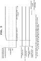
- Fig. 5 shows the light input level andthe output of the autocorrelation detector 201 at the time only of a noise derived from ASE when a light data signal is cut off or at the time of CW reception in keep alive.
- VN level half
- the out-of-synchronization detector 102 is also allowed to reliably generate an alarm when light is applied because it contains only a noise component.
- the detector is not allowed to generate an alarm.
- the gain of an AGC amplifier or a limiter amplifier for supplying a data signal to a signal cutoff detector or a frequency phase-locked loop for reproducing a clock is large enough, a fixed amplitude can be maintained irrespective of variation of a light input level and even at the cutoff of light input, a fixed amplitude can be maintained by amplifying a thermal noise generated from a preamplifier or the like.
- the gain of an AGC amplifier or a limiter amplifier is set to be low to some extent giving preference to stable operation of the amplifier in many cases.
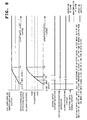
- the AGC amplifier or the limiter amplifier cannot maintain a predetermined amplitude as can be seen from Fig. 7.
- the output of the autocorrelation detector therefore starts decreasing with P4 as a peak, so that from P1 to P3, an alarm can not be generated.
- the detector again generates an alarm.
- the out-of-synchronization detector lacks a data amplitude necessary for stably operating the frequency phase-lock loop to be unable to operate stably. Therefore, there is a shortcoming that between the light input levels P1 and P2, a region is generated where an alarm cannot be reliably generated. Also at the time of a noise derived from ASE when a light data signal is cut off or at the reception of CW in keep alive, a region where an alarm cannot be reliably generated is generated between the light input levels P1 and P2 as shown in Fig. 8.
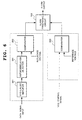
- the signal input cutoff detector of the first embodiment is newly provided with a hysteresis amplifier 501.
- the hysteresis amplifier 501 is an amplifier whose input and output relation has hysteresis characteristics.
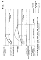
- the hysteresis amplifier 501 By setting the hysteresis amplifier 501 to have an appropriate hysteresis width, effects of noise power when applied light signal power is small can be reduced. In other words, when a superposed noise is less than the hysteresis width, the output of the hysteresis amplifier 501 remains unchanged, so that noise applied to the autocorrelation detector 201 as a random pattern independent of a data signal will be reduced. Furthermore, since a mean value of a signal component draws near to zero with the decrease of a light input level, the output of the autocorrelation detector 201 will be decreased monotonously with the light input level as shown in Fig. 9. Therefore, at the comparator 202, it is only necessary to set one reference voltage (Vref1) at the time of determination of normality/abnormality.
- Vref1 reference voltage
- the out-of-synchronization detector Since the out-of-synchronization detector has its operation unstable when the light input is below P2 similarly to the first embodiment, reliable generation of an alarm over all the regions of the light input levels P0 to P4 needs use of both the signal cutoff detector 101 and the out-of-synchronization detector 102. It is clearly understood that at this time, the reference voltage (Vref1) is set such that an alarm generation region of the signal cutoff detector 101 and an alarm generation region of the out-of-synchronization detector 102 overlap with each other.
- the signal cutoff detector 101 and the out-of-synchronization detector 102 should be both used to reliably generate an alarm as shown in Fig. 10.
- the present embodiment enables abnormality occurring places to be grasped to some extent by monitoring outputs of the above-described two circuits in combination. Table therefor is shown in Fig. 11.
- the output of the signal input detector 101 causes generation of an alarm and the output of the out-of-synchronization detector 102 is unstable, for example, it can be seen that input to the photo receiver is cut off.
- Fig. 13 is an example of a structure of a photo receiver using the signal input cutoff detector of the present invention.
- the photo receiver is structured to include a photo detector 10 and a preamplifier 11 for converting a light input signal into an electric signal, an AGC amplifier or limiter amplifier 12 for amplifying an output of the preamplifier 11 to have a predetermined amplitude, a frequency phase-locked loop 20 which contains a VCO and generates a clock synchronized with an output of the AGC amplifier or limiter amplifier 12 (data signal), a discrimination circuit 18 for discriminating the data signal by the clock, a signal cutoff detector 101 for detecting the data signal existing or not, an out-of-synchronization detector 102 responsive to a VCO control signal of the frequency phase-locked loop 20 for detecting out-of-synchronization, and an alarm processing circuit for processing an alarm from the signal cutoff detector 101 and an alarm from the out-of-synchronization detector 102.
- the signal input cutoff detector As described in the foregoing, being provided with a signal cutoff detector and an out-of-synchronization detector to combine alarm outputs of both the detectors, the signal input cutoff detector according to the present invention enables reliable generation of an alarm against a possible failure at a photo receiver, thereby grasping abnormality occurring places to some extent.
Landscapes
- Physics & Mathematics (AREA)
- Electromagnetism (AREA)
- Engineering & Computer Science (AREA)
- Computer Networks & Wireless Communication (AREA)
- Signal Processing (AREA)
- Synchronisation In Digital Transmission Systems (AREA)
- Optical Communication System (AREA)
- Manipulation Of Pulses (AREA)
- Dc Digital Transmission (AREA)
Abstract
Description
the at least one predetermined reference voltage including a first reference voltage having a value between the mean value obtained when the data signal is large enough and zero, and a second reference voltage higher than the mean value obtained when the data signal is large enough.
which delay time may preferably be half a time length of one bit of the data signal.
alarm processing step of generating a third alarm signal according to generation conditions of the first alarm signal and second alarm signal.
second comparison step of comparing a VCO control signal which controls a voltage controlled oscillator (VCO) to have a frequency and a phase synchronized with the data signal and a predetermined reference voltage and when the VCO control signal is larger, outputting the second alarm signal.
alarm processing step of generating a third alarm signal according to generation conditions of the first alarm signal and second alarm signal.
second comparison step of comparing a VCO control signal which controls a voltage controlled oscillator (VCO) to have a frequency and a phase synchronized with the data signal and a predetermined reference voltage and when the VCO control signal is larger, outputting the second alarm.
outputs a signal indicating that an abnormality occurs.
Claims (26)
- A signal input cutoff detector comprising:a signal cutoff detector (101) which detects a level of a data signal converted from a light input signal into an electric signal and when the level is below a predetermined value, generates a first alarm signal; andan out-of-synchronization (102) detector which monitors a VCO control signal which controls a voltage controlled oscillator (VCO) to have a frequency and a phase synchronized with said data signal and when a level of the control signal exceeds a predetermined value, generates a second alarm signal.
- The signal input cutoff detector as set forth in claim 1, further comprising an alarm processor (103) which generates a third alarm signal according to generation conditions of said first alarm signal and second alarm signal.
- The signal input cutoff detector as set forth in claim 1 or 2, whereinsaid signal cutoff detector (101) includes an autocorrelation detector (201) which calculates an autocorrelation of said data signal to output an autocorrelation signal, anda first comparator (202) which compares said autocorrelation signal with at least one predetermined reference voltage and when said autocorrelation signal is larger, outputs said first alarm signal.
- The signal output cutoff detector as set forth in any one of claims 1 to 3, whereinsaid autocorrelation detector (201) includes a delay element (301) which delays said data signal by a predetermined delay time to output a delayed data signal,an exclusive OR circuit (302) which calculates an exclusive OR of said data signal and said delayed data signal to output an exclusive OR signal, anda first integrator (303) which calculates a mean value of said exclusive OR signal.
- The signal input cutoff detector as set forth in claim 4, wherein
said delay time is half a time length of one bit of said data signal. - The signal input cutoff detector as set forth in any one of claims 3 to 5, whereinsaid at least one predetermined reference voltage of said first comparator (202) includesa first reference voltage having a value between said mean value obtained when said data signal is large enough and zero, anda second reference voltage higher than said mean value obtained when said data signal is large enough.
- The signal output cutoff detector as set forth in any one of claims 1 to 6, wherein
said signal cutoff detector (101) further includes
a hysteresis amplifier (501) provided at an input part of said signal cutoff detector. - The signal input cutoff detector as set forth in any one of claims 1 to 7, wherein
said out-of-synchronization detector (102) includes
a second comparator (203) which compares a VCO control signal which controls a voltage controlled oscillator (VCO) to have a frequency and a phase synchronized with said data signal and a predetermined reference voltage and when the VCO control signal is larger, outputs said second alarm signal. - A photo receiver comprising:a photo detector (10) which converts a light input signal into an electric signal,an amplifier (12) which amplifies said electric signal to have a predetermined amplitude,a frequency phase-locked loop (20) which contains a VCO and generates a clock synchronized with an output of said amplifier and a discrimination circuit for discriminating an output of said amplifier by said clock, anda signal input cutoff detector, whereinsaid signal input cutoff detector includesa signal cutoff detector (101) which detects a level of a data signal converted from a light input signal into an electric signal and when the level is below a predetermined value, generates a first alarm signal, andan out-of-synchronization detector (102) which monitors a VCO control signal which controls a voltage controlled oscillator (VCO) to have a frequency and a phase synchronized with said data signal and when a level of the control signal exceeds a predetermined value, generates a second alarm signal.
- The photo receiver as set forth in claim 9, wherein
said signal input cutoff detector further includes
an alarm processor (103) which generates a third alarm signal according to generation conditions of said first alarm signal and second alarm signal. - The photo receiver as set forth in claim 9 or 10, wherein
said signal cutoff detector (101) includesan autocorrelation detector (201) which calculates an autocorrelation of said data signal to output an autocorrelation signal, anda first comparator (202) which compares said autocorrelation signal with at least one predetermined reference voltage and when said autocorrelation signal is larger, outputs said first alarm signal. - The photo receiver as set forth in any one of claims 9 to 11, wherein
said autocorrelation detector (201) includesa delay element (301) which delays said data signal by a predetermined delay time to output a delayed data signal,an exclusive OR circuit (302) which calculates an exclusive OR of said data signal and said delayed data signal to output an exclusive OR signal, anda first integrator (303) which calculates a mean value of said exclusive OR signal. - The photo receiver as set forth in claim 12, wherein
said delay time is half a time length of one bit of said data signal. - The photo receiver as set forth in any one of claims 11 to 13, whereinsaid at least one predetermined reference voltage of said first comparator (202) includesa first reference voltage having a value between said mean value obtained when said data signal is large enough and zero, anda second reference voltage higher than said mean value obtained when said data signal is large enough.
- The photo receiver as set forth in any one of claims 9 to 14, wherein
said signal cutoff detector (101) further includes
a hysteresis amplifier (501) provided at an input part of said signal cutoff detector. - The photo receiver as set forth in any one of claims 9 to 15, wherein
said out-of-synchronization detector (102) includes
a second comparator (203) which compares a VCO control signal which controls a voltage controlled oscillator (VCO) to have a frequency and a phase synchronized with said data signal and a predetermined reference voltage and when the VCO control signal is larger, outputs said second alarm signal. - A signal output cutoff detecting method comprising the steps of:detecting a level of a data signal converted from a light input signal into an electric signal and when the level is below a predetermined value, generating a first alarm signal, andmonitoring a VCO control signal which controls a voltage controlled oscillator (VCO) to have a frequency and a phase synchronized with said data signal andwhen a level of the control signal exceeds a predetermined value, generating a second alarm signal.
- The signal input cutoff detecting method as set forth in claim 17, further comprising
an alarm processing step of generating a third alarm signal according to generation conditions of said first alarm signal and second alarm signal. - The signal input cutoff detecting method as set forth in claim 17 or 18, wherein
said signal input cutoff detection step includes:an autocorrelation input cutoff detection step of calculating an autocorrelation of said data signal to output an autocorrelation signal, anda first comparison step of comparing said autocorrelation signal with at least one predetermined reference voltage and when said autocorrelation signal is larger, outputting said first alarm signal. - The signal input cutoff detecting method as set forth in claim 19, wherein
said at least one predetermined reference voltage of said first comparison step includes:a first reference voltage having a value between said mean value obtained when said data signal is large enough and zero, anda second reference voltage higher than said mean value obtained when said data signal is large enough. - The signal input cutoff detecting method as set forth in any one of claims 17 to 20, wherein
said out-of-synchronization detection step includes
a second comparison step of comparing a VCO control signal which controls a voltage controlled oscillator (VCO) to have a frequency and a phase synchronized with said data signal and a predetermined reference voltage and when the VCO control signal is larger, outputting said second alarm signal. - A photo receiving method comprising:a step of converting a light input signal into an electric signal and amplifying the converted signal to have a predetermined amplitude,a step of, with a VCO contained, generating a clock synchronized with a data signal amplified to said predetermined amplitude,a step of discriminating a data signal amplified to said predetermined amplitude by said clock,a signal input cutoff detection step of detecting a level of a data signal converted from a light input signal into an electric signal and when the level is below a predetermined value, generating a first alarm signal, andan out-of-synchronization detection step of monitoring a VCO control signal which controls a voltage controlled oscillator (VCO) to have a frequency and a phase synchronized with said data signal and when a level of the control signal exceeds a predetermined value, generating a second alarm signal.
- The photo receiving method as set forth in claim 22, further comprising
an alarm processing step of generating a third alarm signal according to generation conditions of said first alarm signal and second alarm signal. - The photo receiving method as set forth in claims 22 or 23, wherein
said signal input cutoff detection step includes:autocorrelation detection step of calculating an autocorrelation of said data signal to output an autocorrelation signal, andfirst comparison step of comparing said autocorrelation signal with at least one predetermined reference voltage and when said autocorrelation signal is larger, outputting said first alarm signal. - The photo receiving method as set forth in claim 24, wherein
said at least one predetermined reference voltage of said first comparison step includesa first reference voltage having a value between said mean value obtained when said data signal is large enough and zero, anda second reference voltage higher than said mean value obtained when said data signal is large enough. - The photo receiving method as set forth in any one of claims 22 to 25, wherein
said out-of-synchronization detection step includes
a second comparison step of comparing a VCO control signal which controls a voltage controlled oscillator (VCO) to have a frequency and a phase synchronized with said data signal and a predetermined reference voltage and when the VCO control signal is larger, outputting said second alarm signal.
Applications Claiming Priority (2)
| Application Number | Priority Date | Filing Date | Title |
|---|---|---|---|
| JP2000155797A JP3541781B2 (en) | 2000-05-26 | 2000-05-26 | Signal input disconnection detector, optical receiver, and signal input disconnection detection method |
| JP2000155797 | 2000-05-26 |
Publications (2)
| Publication Number | Publication Date |
|---|---|
| EP1158703A2 true EP1158703A2 (en) | 2001-11-28 |
| EP1158703A3 EP1158703A3 (en) | 2003-10-29 |
Family
ID=18660678
Family Applications (1)
| Application Number | Title | Priority Date | Filing Date |
|---|---|---|---|
| EP01250186A Withdrawn EP1158703A3 (en) | 2000-05-26 | 2001-05-26 | Signal input cutoff detector, optical receiver and signal input cutoff detecting method |
Country Status (4)
| Country | Link |
|---|---|
| US (1) | US6570148B2 (en) |
| EP (1) | EP1158703A3 (en) |
| JP (1) | JP3541781B2 (en) |
| CA (1) | CA2348731A1 (en) |
Cited By (3)
| Publication number | Priority date | Publication date | Assignee | Title |
|---|---|---|---|---|
| US7302188B2 (en) | 2002-01-30 | 2007-11-27 | Mitsubishi Denki Kabushiki Kaisha | Disperse equalizer and disperse equalizing method |
| CN101610403B (en) * | 2009-07-21 | 2011-01-12 | 陈苏南 | Remote monitoring and controlling type optical receiver |
| EP2662745A4 (en) * | 2011-07-06 | 2015-01-14 | Mitsubishi Electric Corp | SIGNAL PROCESSING DEVICE |
Families Citing this family (7)
| Publication number | Priority date | Publication date | Assignee | Title |
|---|---|---|---|---|
| JP2003158493A (en) * | 2001-11-21 | 2003-05-30 | Mitsubishi Electric Corp | Optical blockage detection apparatus, optical receiver, optical transmitter, and optical blockage detection method |
| US6919741B2 (en) * | 2003-09-08 | 2005-07-19 | Asia Optical Co., Ltd | Clock down sensor |
| JP2007189294A (en) * | 2006-01-11 | 2007-07-26 | Nec Corp | System, circuit and method for signal detection, and program |
| JP2008153718A (en) * | 2006-12-14 | 2008-07-03 | Meidensha Corp | Clock signal stop decision circuit |
| RU2360659C1 (en) * | 2007-12-21 | 2009-07-10 | Руслан Борисович Айдаров | Mechanotherapeutic apparatus used in treatment and prevention of spinal disorders |
| JP5386760B2 (en) * | 2009-10-21 | 2014-01-15 | 住友電工デバイス・イノベーション株式会社 | Optical receiver module and input disconnection signal output method |
| JP2021097272A (en) * | 2019-12-13 | 2021-06-24 | 株式会社リコー | Data processing apparatus, image reading device, image forming apparatus, and data processing method |
Family Cites Families (7)
| Publication number | Priority date | Publication date | Assignee | Title |
|---|---|---|---|---|
| FR2475826A1 (en) * | 1980-02-12 | 1981-08-14 | Lignes Telegraph Telephon | ALARM TRIGGER DEVICE FOR TRANSMISSION LEVEL INSUFFICIENCY, FOR A RECEIVER MODULE OF AN OPTICAL FIBER TRANSMISSION SYSTEM |
| JPS62126731A (en) * | 1985-11-27 | 1987-06-09 | Nec Corp | Clock recovery circuit |
| US4893002A (en) * | 1986-12-22 | 1990-01-09 | Ag Communications Systems Corporation | Loss of optical input circuit |
| JPH0795156A (en) * | 1993-09-20 | 1995-04-07 | Fujitsu Ltd | Optical input break detection circuit |
| JP2976874B2 (en) * | 1996-03-08 | 1999-11-10 | 日本電気株式会社 | Optical receiver |
| US6178025B1 (en) * | 1997-12-03 | 2001-01-23 | Nortel Networks Limited | Optical network loss-of-signal detection |
| JP2000165323A (en) * | 1998-11-30 | 2000-06-16 | Nec Corp | Optical output-interrupt detection circuit |
-
2000
- 2000-05-26 JP JP2000155797A patent/JP3541781B2/en not_active Expired - Fee Related
-
2001
- 2001-05-25 US US09/864,306 patent/US6570148B2/en not_active Expired - Fee Related
- 2001-05-25 CA CA002348731A patent/CA2348731A1/en not_active Abandoned
- 2001-05-26 EP EP01250186A patent/EP1158703A3/en not_active Withdrawn
Cited By (3)
| Publication number | Priority date | Publication date | Assignee | Title |
|---|---|---|---|---|
| US7302188B2 (en) | 2002-01-30 | 2007-11-27 | Mitsubishi Denki Kabushiki Kaisha | Disperse equalizer and disperse equalizing method |
| CN101610403B (en) * | 2009-07-21 | 2011-01-12 | 陈苏南 | Remote monitoring and controlling type optical receiver |
| EP2662745A4 (en) * | 2011-07-06 | 2015-01-14 | Mitsubishi Electric Corp | SIGNAL PROCESSING DEVICE |
Also Published As
| Publication number | Publication date |
|---|---|
| JP2001339347A (en) | 2001-12-07 |
| US6570148B2 (en) | 2003-05-27 |
| CA2348731A1 (en) | 2001-11-26 |
| JP3541781B2 (en) | 2004-07-14 |
| EP1158703A3 (en) | 2003-10-29 |
| US20010048067A1 (en) | 2001-12-06 |
Similar Documents
| Publication | Publication Date | Title |
|---|---|---|
| US5703711A (en) | In-line optical amplifier | |
| US6684033B1 (en) | Bit rate detection circuit and algorithm for optical networks | |
| US6498670B2 (en) | Optical receiving apparatus and method | |
| JP4528827B2 (en) | Light input break detector | |
| US7881608B2 (en) | Methods and apparatuses for measuring jitter in a transceiver module | |
| EP0910192A2 (en) | Clock extraction circuit | |
| US6570148B2 (en) | Signal input cutoff detector, photo receiver and signal input cutoff detecting method | |
| US7212748B2 (en) | Frequency detection circuit, optical receiver and optical transmission system using the same | |
| JP4900481B2 (en) | Wavelength division multiplexing apparatus and optical signal input interruption detection method | |
| US5805319A (en) | Circuit for discriminating the presence of extraordinariness in an output signal | |
| US8798459B2 (en) | Optical receiver and method of detecting loss of optical signal of the optical receiver | |
| US6795657B1 (en) | Circuit and method for monitoring optical signal level | |
| JPH10209975A (en) | Optical receiver | |
| US20020080456A1 (en) | Input interruption detecting circuit of optical receiver | |
| JP2007181048A (en) | Signal light processing equipment | |
| US9203522B2 (en) | Phase lock loop control for digital communication systems | |
| JPH10229365A (en) | Optical input interruption detection system | |
| JP4375373B2 (en) | Frequency detection circuit, optical receiver using the same, and optical transmission system | |
| JPH10209967A (en) | Optical amplifier alarm circuit | |
| KR100273645B1 (en) | Apparatus for detecting loss of signal in optical reciever | |
| JP2003179654A (en) | Reception quality monitoring circuit | |
| JPH04135343A (en) | Light receiving system | |
| JPH0340540A (en) | Optical signal input disconnection detector for optical signal receiver | |
| JPH06132599A (en) | Optical communication device and optical repeater | |
| JPS612438A (en) | optical receiver circuit |
Legal Events
| Date | Code | Title | Description |
|---|---|---|---|
| PUAI | Public reference made under article 153(3) epc to a published international application that has entered the european phase |
Free format text: ORIGINAL CODE: 0009012 |
|
| AK | Designated contracting states |
Kind code of ref document: A2 Designated state(s): AT BE CH CY DE DK ES FI FR GB GR IE IT LI LU MC NL PT SE TR |
|
| AX | Request for extension of the european patent |
Free format text: AL;LT;LV;MK;RO;SI |
|
| PUAL | Search report despatched |
Free format text: ORIGINAL CODE: 0009013 |
|
| AK | Designated contracting states |
Kind code of ref document: A3 Designated state(s): AT BE CH CY DE DK ES FI FR GB GR IE IT LI LU MC NL PT SE TR |
|
| AX | Request for extension of the european patent |
Extension state: AL LT LV MK RO SI |
|
| 17P | Request for examination filed |
Effective date: 20031111 |
|
| D17P | Request for examination filed (deleted) | ||
| 17Q | First examination report despatched |
Effective date: 20040402 |
|
| AKX | Designation fees paid |
Designated state(s): DE DK FR IT |
|
| D17P | Request for examination filed (deleted) | ||
| STAA | Information on the status of an ep patent application or granted ep patent |
Free format text: STATUS: THE APPLICATION IS DEEMED TO BE WITHDRAWN |
|
| 18D | Application deemed to be withdrawn |
Effective date: 20040430 |