EP1158347A2 - Liquid crystal device and electronic device - Google Patents
Liquid crystal device and electronic device Download PDFInfo
- Publication number
- EP1158347A2 EP1158347A2 EP01304507A EP01304507A EP1158347A2 EP 1158347 A2 EP1158347 A2 EP 1158347A2 EP 01304507 A EP01304507 A EP 01304507A EP 01304507 A EP01304507 A EP 01304507A EP 1158347 A2 EP1158347 A2 EP 1158347A2
- Authority
- EP
- European Patent Office
- Prior art keywords
- liquid crystal
- light emitting
- flexible substrate
- light
- emitting device
- Prior art date
- Legal status (The legal status is an assumption and is not a legal conclusion. Google has not performed a legal analysis and makes no representation as to the accuracy of the status listed.)
- Granted
Links
- 239000004973 liquid crystal related substance Substances 0.000 title claims abstract description 219
- 239000000758 substrate Substances 0.000 claims abstract description 204
- 238000005286 illumination Methods 0.000 abstract description 5
- 230000009467 reduction Effects 0.000 abstract description 5
- 239000010408 film Substances 0.000 description 44
- 229910052751 metal Inorganic materials 0.000 description 28
- 239000002184 metal Substances 0.000 description 28
- 239000011159 matrix material Substances 0.000 description 13
- 238000010276 construction Methods 0.000 description 12
- 230000005684 electric field Effects 0.000 description 11
- 230000006870 function Effects 0.000 description 8
- 239000003990 capacitor Substances 0.000 description 6
- 239000000463 material Substances 0.000 description 6
- 230000003247 decreasing effect Effects 0.000 description 5
- 238000000034 method Methods 0.000 description 5
- 238000000151 deposition Methods 0.000 description 4
- 238000009792 diffusion process Methods 0.000 description 4
- 238000003860 storage Methods 0.000 description 4
- 239000004642 Polyimide Substances 0.000 description 3
- 229910052782 aluminium Inorganic materials 0.000 description 3
- XAGFODPZIPBFFR-UHFFFAOYSA-N aluminium Chemical compound [Al] XAGFODPZIPBFFR-UHFFFAOYSA-N 0.000 description 3
- KRKNYBCHXYNGOX-UHFFFAOYSA-N citric acid Chemical compound OC(=O)CC(O)(C(O)=O)CC(O)=O KRKNYBCHXYNGOX-UHFFFAOYSA-N 0.000 description 3
- 238000013461 design Methods 0.000 description 3
- 230000010365 information processing Effects 0.000 description 3
- 239000012212 insulator Substances 0.000 description 3
- 230000003647 oxidation Effects 0.000 description 3
- 238000007254 oxidation reaction Methods 0.000 description 3
- BPUBBGLMJRNUCC-UHFFFAOYSA-N oxygen(2-);tantalum(5+) Chemical compound [O-2].[O-2].[O-2].[O-2].[O-2].[Ta+5].[Ta+5] BPUBBGLMJRNUCC-UHFFFAOYSA-N 0.000 description 3
- 239000002245 particle Substances 0.000 description 3
- 229920001721 polyimide Polymers 0.000 description 3
- 230000008569 process Effects 0.000 description 3
- 239000010409 thin film Substances 0.000 description 3
- VYZAMTAEIAYCRO-UHFFFAOYSA-N Chromium Chemical compound [Cr] VYZAMTAEIAYCRO-UHFFFAOYSA-N 0.000 description 2
- ZOKXTWBITQBERF-UHFFFAOYSA-N Molybdenum Chemical compound [Mo] ZOKXTWBITQBERF-UHFFFAOYSA-N 0.000 description 2
- 229910001362 Ta alloys Inorganic materials 0.000 description 2
- 229910052804 chromium Inorganic materials 0.000 description 2
- 239000011651 chromium Substances 0.000 description 2
- 239000011248 coating agent Substances 0.000 description 2
- 238000000576 coating method Methods 0.000 description 2
- 230000008021 deposition Effects 0.000 description 2
- 239000000428 dust Substances 0.000 description 2
- 230000005611 electricity Effects 0.000 description 2
- 239000004744 fabric Substances 0.000 description 2
- 239000011521 glass Substances 0.000 description 2
- 238000009499 grossing Methods 0.000 description 2
- 229910052750 molybdenum Inorganic materials 0.000 description 2
- 239000011733 molybdenum Substances 0.000 description 2
- 238000000059 patterning Methods 0.000 description 2
- 238000000206 photolithography Methods 0.000 description 2
- 239000004033 plastic Substances 0.000 description 2
- 239000000243 solution Substances 0.000 description 2
- 230000003068 static effect Effects 0.000 description 2
- 229910052715 tantalum Inorganic materials 0.000 description 2
- GUVRBAGPIYLISA-UHFFFAOYSA-N tantalum atom Chemical compound [Ta] GUVRBAGPIYLISA-UHFFFAOYSA-N 0.000 description 2
- WFKWXMTUELFFGS-UHFFFAOYSA-N tungsten Chemical compound [W] WFKWXMTUELFFGS-UHFFFAOYSA-N 0.000 description 2
- 229910052721 tungsten Inorganic materials 0.000 description 2
- 239000010937 tungsten Substances 0.000 description 2
- 229910052692 Dysprosium Inorganic materials 0.000 description 1
- 239000004593 Epoxy Substances 0.000 description 1
- RTAQQCXQSZGOHL-UHFFFAOYSA-N Titanium Chemical compound [Ti] RTAQQCXQSZGOHL-UHFFFAOYSA-N 0.000 description 1
- 239000000654 additive Substances 0.000 description 1
- 230000000996 additive effect Effects 0.000 description 1
- 239000000853 adhesive Substances 0.000 description 1
- 230000001070 adhesive effect Effects 0.000 description 1
- 239000007864 aqueous solution Substances 0.000 description 1
- 238000005452 bending Methods 0.000 description 1
- 230000015572 biosynthetic process Effects 0.000 description 1
- 230000008859 change Effects 0.000 description 1
- 238000006243 chemical reaction Methods 0.000 description 1
- 239000003086 colorant Substances 0.000 description 1
- 239000004020 conductor Substances 0.000 description 1
- 238000012937 correction Methods 0.000 description 1
- 230000007423 decrease Effects 0.000 description 1
- 230000007547 defect Effects 0.000 description 1
- 238000010586 diagram Methods 0.000 description 1
- KBQHZAAAGSGFKK-UHFFFAOYSA-N dysprosium atom Chemical compound [Dy] KBQHZAAAGSGFKK-UHFFFAOYSA-N 0.000 description 1
- 238000009429 electrical wiring Methods 0.000 description 1
- 238000005530 etching Methods 0.000 description 1
- 238000002474 experimental method Methods 0.000 description 1
- 238000010438 heat treatment Methods 0.000 description 1
- 239000012535 impurity Substances 0.000 description 1
- 238000010348 incorporation Methods 0.000 description 1
- AMGQUBHHOARCQH-UHFFFAOYSA-N indium;oxotin Chemical compound [In].[Sn]=O AMGQUBHHOARCQH-UHFFFAOYSA-N 0.000 description 1
- 238000003780 insertion Methods 0.000 description 1
- 230000037431 insertion Effects 0.000 description 1
- 238000007689 inspection Methods 0.000 description 1
- 229910052746 lanthanum Inorganic materials 0.000 description 1
- FZLIPJUXYLNCLC-UHFFFAOYSA-N lanthanum atom Chemical compound [La] FZLIPJUXYLNCLC-UHFFFAOYSA-N 0.000 description 1
- 238000004519 manufacturing process Methods 0.000 description 1
- 239000000203 mixture Substances 0.000 description 1
- 238000012986 modification Methods 0.000 description 1
- 230000004048 modification Effects 0.000 description 1
- 230000003287 optical effect Effects 0.000 description 1
- 230000001590 oxidative effect Effects 0.000 description 1
- 230000000737 periodic effect Effects 0.000 description 1
- 229920000642 polymer Polymers 0.000 description 1
- 239000010453 quartz Substances 0.000 description 1
- 230000004043 responsiveness Effects 0.000 description 1
- 229910052702 rhenium Inorganic materials 0.000 description 1
- WUAPFZMCVAUBPE-UHFFFAOYSA-N rhenium atom Chemical compound [Re] WUAPFZMCVAUBPE-UHFFFAOYSA-N 0.000 description 1
- 238000007789 sealing Methods 0.000 description 1
- 239000003566 sealing material Substances 0.000 description 1
- VYPSYNLAJGMNEJ-UHFFFAOYSA-N silicon dioxide Inorganic materials O=[Si]=O VYPSYNLAJGMNEJ-UHFFFAOYSA-N 0.000 description 1
- 238000005476 soldering Methods 0.000 description 1
- 238000004544 sputter deposition Methods 0.000 description 1
- 239000000126 substance Substances 0.000 description 1
- 229910001936 tantalum oxide Inorganic materials 0.000 description 1
- 229910052719 titanium Inorganic materials 0.000 description 1
- 239000010936 titanium Substances 0.000 description 1
- 230000000007 visual effect Effects 0.000 description 1
- 229910052727 yttrium Inorganic materials 0.000 description 1
- VWQVUPCCIRVNHF-UHFFFAOYSA-N yttrium atom Chemical compound [Y] VWQVUPCCIRVNHF-UHFFFAOYSA-N 0.000 description 1
Images






Classifications
-
- G—PHYSICS
- G02—OPTICS
- G02F—OPTICAL DEVICES OR ARRANGEMENTS FOR THE CONTROL OF LIGHT BY MODIFICATION OF THE OPTICAL PROPERTIES OF THE MEDIA OF THE ELEMENTS INVOLVED THEREIN; NON-LINEAR OPTICS; FREQUENCY-CHANGING OF LIGHT; OPTICAL LOGIC ELEMENTS; OPTICAL ANALOGUE/DIGITAL CONVERTERS
- G02F1/00—Devices or arrangements for the control of the intensity, colour, phase, polarisation or direction of light arriving from an independent light source, e.g. switching, gating or modulating; Non-linear optics
- G02F1/01—Devices or arrangements for the control of the intensity, colour, phase, polarisation or direction of light arriving from an independent light source, e.g. switching, gating or modulating; Non-linear optics for the control of the intensity, phase, polarisation or colour
- G02F1/13—Devices or arrangements for the control of the intensity, colour, phase, polarisation or direction of light arriving from an independent light source, e.g. switching, gating or modulating; Non-linear optics for the control of the intensity, phase, polarisation or colour based on liquid crystals, e.g. single liquid crystal display cells
- G02F1/133—Constructional arrangements; Operation of liquid crystal cells; Circuit arrangements
-
- G—PHYSICS
- G02—OPTICS
- G02F—OPTICAL DEVICES OR ARRANGEMENTS FOR THE CONTROL OF LIGHT BY MODIFICATION OF THE OPTICAL PROPERTIES OF THE MEDIA OF THE ELEMENTS INVOLVED THEREIN; NON-LINEAR OPTICS; FREQUENCY-CHANGING OF LIGHT; OPTICAL LOGIC ELEMENTS; OPTICAL ANALOGUE/DIGITAL CONVERTERS
- G02F1/00—Devices or arrangements for the control of the intensity, colour, phase, polarisation or direction of light arriving from an independent light source, e.g. switching, gating or modulating; Non-linear optics
- G02F1/01—Devices or arrangements for the control of the intensity, colour, phase, polarisation or direction of light arriving from an independent light source, e.g. switching, gating or modulating; Non-linear optics for the control of the intensity, phase, polarisation or colour
- G02F1/13—Devices or arrangements for the control of the intensity, colour, phase, polarisation or direction of light arriving from an independent light source, e.g. switching, gating or modulating; Non-linear optics for the control of the intensity, phase, polarisation or colour based on liquid crystals, e.g. single liquid crystal display cells
- G02F1/133—Constructional arrangements; Operation of liquid crystal cells; Circuit arrangements
- G02F1/1333—Constructional arrangements; Manufacturing methods
- G02F1/1335—Structural association of cells with optical devices, e.g. polarisers or reflectors
- G02F1/1336—Illuminating devices
- G02F1/133615—Edge-illuminating devices, i.e. illuminating from the side
-
- G—PHYSICS
- G02—OPTICS
- G02F—OPTICAL DEVICES OR ARRANGEMENTS FOR THE CONTROL OF LIGHT BY MODIFICATION OF THE OPTICAL PROPERTIES OF THE MEDIA OF THE ELEMENTS INVOLVED THEREIN; NON-LINEAR OPTICS; FREQUENCY-CHANGING OF LIGHT; OPTICAL LOGIC ELEMENTS; OPTICAL ANALOGUE/DIGITAL CONVERTERS
- G02F1/00—Devices or arrangements for the control of the intensity, colour, phase, polarisation or direction of light arriving from an independent light source, e.g. switching, gating or modulating; Non-linear optics
- G02F1/01—Devices or arrangements for the control of the intensity, colour, phase, polarisation or direction of light arriving from an independent light source, e.g. switching, gating or modulating; Non-linear optics for the control of the intensity, phase, polarisation or colour
- G02F1/13—Devices or arrangements for the control of the intensity, colour, phase, polarisation or direction of light arriving from an independent light source, e.g. switching, gating or modulating; Non-linear optics for the control of the intensity, phase, polarisation or colour based on liquid crystals, e.g. single liquid crystal display cells
- G02F1/133—Constructional arrangements; Operation of liquid crystal cells; Circuit arrangements
- G02F1/1333—Constructional arrangements; Manufacturing methods
- G02F1/1345—Conductors connecting electrodes to cell terminals
- G02F1/13452—Conductors connecting driver circuitry and terminals of panels
-
- G—PHYSICS
- G02—OPTICS
- G02F—OPTICAL DEVICES OR ARRANGEMENTS FOR THE CONTROL OF LIGHT BY MODIFICATION OF THE OPTICAL PROPERTIES OF THE MEDIA OF THE ELEMENTS INVOLVED THEREIN; NON-LINEAR OPTICS; FREQUENCY-CHANGING OF LIGHT; OPTICAL LOGIC ELEMENTS; OPTICAL ANALOGUE/DIGITAL CONVERTERS
- G02F1/00—Devices or arrangements for the control of the intensity, colour, phase, polarisation or direction of light arriving from an independent light source, e.g. switching, gating or modulating; Non-linear optics
- G02F1/01—Devices or arrangements for the control of the intensity, colour, phase, polarisation or direction of light arriving from an independent light source, e.g. switching, gating or modulating; Non-linear optics for the control of the intensity, phase, polarisation or colour
- G02F1/13—Devices or arrangements for the control of the intensity, colour, phase, polarisation or direction of light arriving from an independent light source, e.g. switching, gating or modulating; Non-linear optics for the control of the intensity, phase, polarisation or colour based on liquid crystals, e.g. single liquid crystal display cells
- G02F1/133—Constructional arrangements; Operation of liquid crystal cells; Circuit arrangements
- G02F1/136—Liquid crystal cells structurally associated with a semi-conducting layer or substrate, e.g. cells forming part of an integrated circuit
- G02F1/1362—Active matrix addressed cells
- G02F1/1365—Active matrix addressed cells in which the switching element is a two-electrode device
Definitions
- the present invention relates to a liquid crystal device in which light transmitted through a liquid crystal is modulated by controlling the orientation of the liquid crystal to display an image.
- the present invention also relates to an electronic device using the liquid crystal device.
- a second object of the present invention is to prevent deviation of the position of a light emitting device relative to a light guide to prevent the occurrence of variation in the efficiency of light incidence on the light guide even when a supporting structure for the light emitting device is simplified, thereby preventing the occurrence of variation in the light supplied to a liquid crystal.
- liquid crystal devices are possibly distinguished into an active matrix system liquid crystal device in which pixel electrodes are driven by switching elements (namely, nonlinear elements), and a passive matrix system liquid crystal device in which pixel electrodes are formed in a simple matrix arrangement without using switching elements.
- the active matrix system is thought to be advantageous from the viewpoint of good contrast and responsiveness, and ease of achievement of a high-definition display.
- Known systems of the active matrix system liquid crystal device include a system using a three-terminal element such as a thin film transistor (TFT) as a switching element, and a system using a two-terminal element such as a thin film diode (TFD) .
- TFT thin film transistor
- TFD thin film diode
- Fig. 3 schematically shows the electric construction of the liquid crystal panel 2.
- a plurality of scanning lines 51 are formed in the line direction (X direction) on the liquid crystal panel 2
- a plurality of data lines 52 are formed in the column direction (Y direction)
- a pixel 53 being formed at each of the intersections of the scanning lines 51 and the data lines 52.
- Each of the pixels 53 is formed by series connection of the liquid crystal layer 54 and the TFD (Thin Film Diode).
- the first metal film 62 is made of, for example, a tantalum single material, or a tantalum alloy. Although the thickness of the first metal film 62 is appropriately selected according to the application of the TFD 56, the thickness is usually about 100 to 500 nm.
- an element in the VI to VIII group in the periodic table such as tungsten, chromium, molybdenum, rhenium, yttrium, lanthanum, or dysprosium, is added to tantalum as the main component. In this case, tungsten is preferred as the additive element, and the content is preferably, for example, 0.1 to 6% by weight.
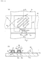
- each of the apertures 67 formed in the pixel electrodes 66 are described.
- the distance between both substrates is generally several ⁇ m.
- black display is made by the influence of a leakage electric field from one end of the periphery of each electrode with the voltage applied.
- the transmissive display and the reflective display can be balanced well when the area of the apertures 67 is set to 10 to 25 % of the area of the pixel electrodes 66.
- the area of the pixel electrodes 66 means the area of the effective display regions which are the intersections of the pixel electrodes 66 and the data lines 52, and which are not shielded by the black matrix, or the like.
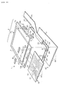
- a wide space R can be formed between the light guide 4A and the FPC 3a so that the space R can be desirably used for containing, for example, a chip capacitor and other electronic parts mounted on the FPC 3a.
- the present invention is applied to an active matrix liquid crystal device of a transflective type using TFDs.
- the present invention can be applied to other various types of liquid crystal devices, such as a reflective liquid crystal device, a transmissive liquid crystal device, an active matrix liquid crystal device using switching elements other than TFDs, a passive matrix liquid crystal device not using switching elements.
Landscapes
- Physics & Mathematics (AREA)
- Nonlinear Science (AREA)
- Mathematical Physics (AREA)
- Chemical & Material Sciences (AREA)
- Crystallography & Structural Chemistry (AREA)
- General Physics & Mathematics (AREA)
- Optics & Photonics (AREA)
- Liquid Crystal (AREA)
- Planar Illumination Modules (AREA)
- Devices For Indicating Variable Information By Combining Individual Elements (AREA)
- Fastening Of Light Sources Or Lamp Holders (AREA)
- Liquid Crystal Substances (AREA)
Abstract
Description
Claims (19)
- A liquid crystal device comprising a pair of substrates which hold a liquid crystal therebetween, a light guide provided opposite to one of the substrates, a flexible substrate connected to one of the substrates, and a light emitting device provided opposite to a light receiving surface of the light guide;
wherein the light emitting device is mounted on the flexible substrate and arranged opposite to the light receiving surface of the light guide. - The liquid crystal device according to Claim 1, wherein the flexible substrate is bent along the light receiving surface of the light guide so that the light emitting device is arranged opposite to the light receiving surface.
- The liquid crystal device according to Claim 1 or 2, wherein the flexible substrate has a terminal to be connected to one of the substrates, the light emitting device provided on the same surface of the flexible substrate as the surface where the terminal is provided, and a wiring pattern provided on the surface opposite to the surface where the light emitting device is provided, the wiring pattern being connected to the terminal through a through hole.
- The liquid crystal device according to Claim 1 or 2, wherein the flexible substrate has a terminal to be connected to one of the substrates, a wiring pattern formed on the same surface as the surface on which the terminal is provided, and the light emitting device provided on the same surface of the flexible substrate as the surface on which the wiring pattern is provided.
- The liquid crystal device according to Claim 4, wherein the wiring pattern is provided on the flexible substrate to avoid the light emitting device.
- The liquid crystal device according to any one of Claims 1 to 5, wherein the light emitting surface is at the side of the mounted surface of the light emitting device to the flexible substrate, and the light emitting surface is arranged opposite to the light receiving surface of the light guide.
- The liquid crystal device according to any one of Claims 1 to 5, wherein the light guide is formed in a bent shape so that the light receiving surface thereof faces to the direction opposite to the pair of substrates, and the light emitting surface of the light emitting device is arranged opposite to the light receiving surface facing to the direction opposite to the pair of substrates.
- The liquid crystal device according to any one of Claims 1 to 7, wherein the flexible substrate is used for supplying a signal for driving the liquid crystal.
- A liquid crystal device comprising a pair of substrates which hold a liquid crystal therebetween, a light guide provided opposite to one of the substrates, a flexible substrate connected to one of the substrates, and a light emitting device provided opposite to the light receiving surface of the light guide;
wherein the light emitting device is mounted on the flexible substrate and arranged opposite to the light receiving surface; and
positioning means is provided between the light emitting device and the light receiving surface of the light guide, for positioning the light emitting device. - The liquid crystal device according to Claim 9, wherein the positioning means comprises a projecting portion provided on one of the light emitting device side and the light guide side, and a recessed portion provided on the other side to be engaged with the projecting portion.
- The liquid crystal device according to Claim 10, wherein the projecting portion comprises a cylindrical pin or a triangular prism projection.
- The liquid crystal device according to any one of Claims 9 to 11, wherein the flexible substrate is bent along the light receiving surface of the light guide so that the light emitting device is arranged opposite to the light receiving surface.
- The liquid crystal device according to any one of Claims 9 to 12, wherein the flexible substrate has a terminal to be connected to one of the substrates, the light emitting device provided on the same surface of the flexible substrate as the surface where the terminal is provided, and a wiring pattern provided on the surface opposite to the surface where the light emitting device is provided, the wiring pattern being connected to the terminal through a through hole.
- The liquid crystal device according to any one of Claims 9 to 12, wherein the flexible substrate has a terminal to be connected to the substrate, a wiring pattern formed on the same surface as the surface on which the terminal is provided, and the light emitting device provided on the same surface of the flexible substrate as the surface on which the wiring pattern is provided.
- The liquid crystal device according to Claim 14, wherein the wiring pattern is provided on the flexible substrate to avoid the light emitting device.
- The liquid crystal device according to any one of Claims 9 to 15, wherein the light emitting surface is at the side of the mounted surface of the light emitting device to the flexible substrate , and the light emitting surface is arranged opposite to the light receiving surface of the light guide.
- The liquid crystal device according to any one of Claims 9 to 15, wherein the light guide is formed in a bent shape so that the light receiving surface thereof faces to the direction opposite to the pair of substrates, and the light emitting surface of the light emitting device is arranged opposite to the light receiving surface facing to the direction opposite to the pair of substrates.
- The liquid crystal device according to any one of Claims 9 to 17, wherein the flexible substrate is used for supplying a signal for driving the liquid crystal.
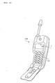
- An electronic device comprising a liquid crystal device, and a control circuit for controlling an operation of the liquid crystal device, wherein the liquid crystal device is a liquid crystal device in accordance with any one of Claims 1 to 18, and the flexible substrate is connected to the control circuit so that the light emitting device is arranged opposite to the light receiving surface of the light guide with the control circuit connected to the flexible substrate.
Applications Claiming Priority (2)
| Application Number | Priority Date | Filing Date | Title |
|---|---|---|---|
| JP2000151666 | 2000-05-23 | ||
| JP2000151666A JP3642263B2 (en) | 2000-05-23 | 2000-05-23 | Liquid crystal device and electronic device |
Publications (3)
| Publication Number | Publication Date |
|---|---|
| EP1158347A2 true EP1158347A2 (en) | 2001-11-28 |
| EP1158347A3 EP1158347A3 (en) | 2002-11-27 |
| EP1158347B1 EP1158347B1 (en) | 2006-08-02 |
Family
ID=18657187
Family Applications (1)
| Application Number | Title | Priority Date | Filing Date |
|---|---|---|---|
| EP01304507A Expired - Lifetime EP1158347B1 (en) | 2000-05-23 | 2001-05-22 | Liquid crystal device and electronic device |
Country Status (8)
| Country | Link |
|---|---|
| US (1) | US6897912B2 (en) |
| EP (1) | EP1158347B1 (en) |
| JP (1) | JP3642263B2 (en) |
| KR (1) | KR100441327B1 (en) |
| CN (1) | CN1208667C (en) |
| AT (1) | ATE335219T1 (en) |
| DE (1) | DE60121858T2 (en) |
| TW (1) | TWI291064B (en) |
Cited By (4)
| Publication number | Priority date | Publication date | Assignee | Title |
|---|---|---|---|---|
| GB2374713A (en) * | 2001-01-16 | 2002-10-23 | Visteon Global Tech Inc | Flexible led backlighting circuit |
| EP1510853A1 (en) | 2003-08-27 | 2005-03-02 | NEC Corporation | Liquid crystal display module, mobile communication device, and method of mounting liquid crystal display module |
| CN100368895C (en) * | 2006-05-30 | 2008-02-13 | 友达光电股份有限公司 | Backlight module using light emitting diode |
| EP1903377A1 (en) * | 2006-09-22 | 2008-03-26 | Samsung SDI Co., Ltd. | Flat panel display device and portable display apparatus using the same |
Families Citing this family (45)
| Publication number | Priority date | Publication date | Assignee | Title |
|---|---|---|---|---|
| JP4689851B2 (en) * | 2001-02-23 | 2011-05-25 | Nec液晶テクノロジー株式会社 | Active matrix liquid crystal display device |
| EP1376212A1 (en) * | 2002-06-21 | 2004-01-02 | Asulab S.A. | Display cell, in particular comprising liquid crystals, or photovoltaic cell comprising connection means to a driver circuit |
| JP2004247373A (en) | 2003-02-12 | 2004-09-02 | Semiconductor Energy Lab Co Ltd | Semiconductor device |
| JP4217090B2 (en) * | 2003-03-20 | 2009-01-28 | 株式会社 日立ディスプレイズ | Display device |
| KR20040087464A (en) * | 2003-04-08 | 2004-10-14 | 삼성전자주식회사 | Liquid crystal display device |
| TW594176B (en) * | 2003-06-17 | 2004-06-21 | Au Optronics Corp | Circuit scheme of light emitting device and liquid crystal display |
| JP4543772B2 (en) * | 2003-09-19 | 2010-09-15 | セイコーエプソン株式会社 | Electro-optical device and electronic apparatus |
| JP4072493B2 (en) * | 2003-11-14 | 2008-04-09 | Nec液晶テクノロジー株式会社 | Substrate module and liquid crystal module |
| US7196693B2 (en) * | 2003-12-12 | 2007-03-27 | Compal Electronics, Inc. | Lighting keyboard and lighting module thereof |
| JP4055741B2 (en) | 2004-05-24 | 2008-03-05 | セイコーエプソン株式会社 | Electro-optical device and electronic apparatus |
| JP4072519B2 (en) * | 2004-06-18 | 2008-04-09 | シャープ株式会社 | Lighting device for display device |
| JP4581726B2 (en) * | 2004-12-28 | 2010-11-17 | ソニー株式会社 | Display device and portable device |
| TWM272351U (en) * | 2005-01-21 | 2005-08-01 | Innolux Display Corp | Display module |
| JP4244942B2 (en) | 2005-03-08 | 2009-03-25 | セイコーエプソン株式会社 | Liquid crystal device, lighting device, and electronic device |
| US7284894B2 (en) * | 2005-05-31 | 2007-10-23 | Avago Technologies Eceliip (Singapore) Pte Ltd | Light source utilizing a flexible circuit carrier |
| JP4616105B2 (en) * | 2005-07-20 | 2011-01-19 | 株式会社 日立ディスプレイズ | Liquid crystal display device |
| TW200712684A (en) * | 2005-09-30 | 2007-04-01 | Innolux Display Corp | Liquid crystal display module |
| CN1971345B (en) * | 2005-11-24 | 2010-05-12 | 群康科技(深圳)有限公司 | Flexible printed circuit and LCD |
| CN101401497B (en) * | 2006-02-10 | 2013-01-02 | 诺基亚公司 | A display module and method for fixing |
| TWI326375B (en) * | 2006-04-21 | 2010-06-21 | Chimei Innolux Corp | Liquid crystal display device |
| KR100821043B1 (en) * | 2006-09-22 | 2008-04-08 | 삼성에스디아이 주식회사 | Flexible Printed Circuit Board |
| KR100821042B1 (en) * | 2006-09-22 | 2008-04-08 | 삼성에스디아이 주식회사 | LCD and portable display device using same |
| KR101284053B1 (en) * | 2006-10-26 | 2013-07-10 | 삼성디스플레이 주식회사 | Back-light assembly and display apparatus having the same |
| JP4333727B2 (en) * | 2006-11-13 | 2009-09-16 | エプソンイメージングデバイス株式会社 | ELECTRO-OPTICAL DEVICE, LIGHTING DEVICE, AND ELECTRONIC DEVICE |
| JP5010925B2 (en) * | 2007-01-12 | 2012-08-29 | 株式会社ジャパンディスプレイイースト | LCD module |
| US8157430B2 (en) * | 2007-02-16 | 2012-04-17 | Sharp Kabushiki Kaisha | Backlight device and planar display device using the same |
| TWI330415B (en) * | 2007-04-02 | 2010-09-11 | Chimei Innolux Corp | Light emitting diode and a backlight module using the same |
| CN101281942B (en) * | 2007-04-06 | 2011-06-29 | 群康科技(深圳)有限公司 | LED and backlight module using the same |
| KR100857693B1 (en) | 2007-05-10 | 2008-09-08 | 삼성에스디아이 주식회사 | Liquid crystal display |
| US7707974B2 (en) * | 2007-07-25 | 2010-05-04 | Radio Systems Corporation | LCD window for animal training device and method for manufacture |
| TWM329818U (en) * | 2007-10-17 | 2008-04-01 | Universal Scient Ind Co Ltd | Portable electronic device with anisotropic conductive unit |
| KR101431154B1 (en) * | 2007-11-08 | 2014-08-18 | 삼성디스플레이 주식회사 | Display apparatus and method for assembling the same |
| EP2299316B1 (en) | 2008-07-08 | 2013-03-13 | Sharp Kabushiki Kaisha | Liquid crystal display device |
| US9335579B2 (en) * | 2011-05-18 | 2016-05-10 | Sharp Kabushiki Kaisha | Display device |
| TWI553382B (en) * | 2011-06-24 | 2016-10-11 | Lg伊諾特股份有限公司 | Illumination system |
| KR101346083B1 (en) * | 2012-04-26 | 2013-12-31 | 엘지디스플레이 주식회사 | Display Device |
| KR101307960B1 (en) * | 2012-04-26 | 2013-09-12 | 엘지디스플레이 주식회사 | Display device |
| CN102809100A (en) * | 2012-08-09 | 2012-12-05 | 京东方科技集团股份有限公司 | Backlight and production method thereof |
| US9072167B2 (en) * | 2012-08-27 | 2015-06-30 | Shenzhen China Star Optoelectronics Technology Co., Ltd. | Display device |
| US9084338B2 (en) * | 2012-08-27 | 2015-07-14 | Shenzhen China Star Optoelectronics Technology Co., Ltd. | Display device |
| US8988866B2 (en) * | 2012-08-27 | 2015-03-24 | Shenzhen China Star Optoelectronics Technology Co., Ltd. | Display device |
| US8988875B2 (en) * | 2012-08-27 | 2015-03-24 | Shenzhen China Star Optoelectronics Technology Co., Ltd. | Display device |
| KR102416142B1 (en) * | 2015-08-31 | 2022-07-01 | 엘지디스플레이 주식회사 | Back cover and transparent display apparatus using the same |
| CN108398818B (en) * | 2017-02-06 | 2021-04-27 | 精工爱普生株式会社 | Electro-optical device and electronic apparatus |
| CN113419370B (en) * | 2018-06-06 | 2022-10-18 | 上海中航光电子有限公司 | Liquid crystal display device having a plurality of pixel electrodes |
Family Cites Families (19)
| Publication number | Priority date | Publication date | Assignee | Title |
|---|---|---|---|---|
| US149074A (en) * | 1874-03-31 | Improvement in paint compounds | ||
| JPH01219823A (en) | 1988-02-29 | 1989-09-01 | Seiko Epson Corp | Liquid crystal display device |
| JP2689781B2 (en) * | 1991-08-21 | 1997-12-10 | 三菱電機株式会社 | Lighting structure and assembly structure of liquid crystal display |
| JPH0581877U (en) * | 1992-04-02 | 1993-11-05 | 三洋電機株式会社 | Surface lighting device |
| JPH0590450U (en) | 1992-05-13 | 1993-12-10 | 富士通テン株式会社 | Backlight structure |
| GB2296362B (en) * | 1994-12-23 | 1999-03-03 | Nokia Mobile Phones Ltd | Illuminated LCD apparatus and method of manufacture |
| US5613751A (en) * | 1995-06-27 | 1997-03-25 | Lumitex, Inc. | Light emitting panel assemblies |
| JP3613897B2 (en) * | 1996-03-29 | 2005-01-26 | セイコーエプソン株式会社 | Liquid crystal display device and equipment using the same |
| JP3319279B2 (en) * | 1996-04-23 | 2002-08-26 | セイコーエプソン株式会社 | Liquid crystal display |
| JPH10142426A (en) * | 1996-11-15 | 1998-05-29 | Matsushita Electric Works Ltd | Light transmission member |
| US5708428A (en) * | 1996-12-10 | 1998-01-13 | Ericsson Inc. | Method and apparatus for providing backlighting for keypads and LCD panels |
| JPH10301504A (en) * | 1997-04-24 | 1998-11-13 | Kokusai Electric Co Ltd | LCD module and its mounting method |
| JPH11344705A (en) | 1998-05-29 | 1999-12-14 | Kyocera Corp | LCD backlight method |
| JP3728981B2 (en) * | 1998-08-26 | 2005-12-21 | セイコーエプソン株式会社 | Liquid crystal device and electronic device |
| JP2000075316A (en) | 1998-09-02 | 2000-03-14 | Matsushita Electric Ind Co Ltd | Liquid crystal display module and film carrier and portable terminal equipment |
| JP2000098415A (en) * | 1998-09-28 | 2000-04-07 | Matsushita Electric Ind Co Ltd | Liquid crystal display |
| JP2000235183A (en) * | 1999-02-16 | 2000-08-29 | Matsushita Electric Ind Co Ltd | Illumination device and portable information device having the same |
| JP3645761B2 (en) * | 1999-10-15 | 2005-05-11 | Necアクセステクニカ株式会社 | LCD backlight |
| JP4610037B2 (en) | 2000-03-15 | 2011-01-12 | 京セラ株式会社 | Liquid crystal display device |
-
2000
- 2000-05-23 JP JP2000151666A patent/JP3642263B2/en not_active Expired - Lifetime
-
2001
- 2001-05-03 TW TW090110645A patent/TWI291064B/en not_active IP Right Cessation
- 2001-05-21 KR KR10-2001-0027607A patent/KR100441327B1/en not_active Expired - Lifetime
- 2001-05-22 DE DE60121858T patent/DE60121858T2/en not_active Expired - Lifetime
- 2001-05-22 AT AT01304507T patent/ATE335219T1/en not_active IP Right Cessation
- 2001-05-22 EP EP01304507A patent/EP1158347B1/en not_active Expired - Lifetime
- 2001-05-22 CN CNB011195010A patent/CN1208667C/en not_active Expired - Lifetime
- 2001-05-22 US US09/863,059 patent/US6897912B2/en not_active Expired - Lifetime
Cited By (8)
| Publication number | Priority date | Publication date | Assignee | Title |
|---|---|---|---|---|
| GB2374713A (en) * | 2001-01-16 | 2002-10-23 | Visteon Global Tech Inc | Flexible led backlighting circuit |
| GB2374713B (en) * | 2001-01-16 | 2003-03-19 | Visteon Global Tech Inc | Flexible led backlighting circuit |
| DE10201045B4 (en) * | 2001-01-16 | 2007-11-22 | Visteon Global Technologies, Inc., Dearborn | Flexible LED circuit for backlighting |
| EP1510853A1 (en) | 2003-08-27 | 2005-03-02 | NEC Corporation | Liquid crystal display module, mobile communication device, and method of mounting liquid crystal display module |
| US7403242B2 (en) | 2003-08-27 | 2008-07-22 | Nec Corporation | Liquid crystal display module, mobile communication device, and method of mounting liquid crystal display module |
| CN100368895C (en) * | 2006-05-30 | 2008-02-13 | 友达光电股份有限公司 | Backlight module using light emitting diode |
| EP1903377A1 (en) * | 2006-09-22 | 2008-03-26 | Samsung SDI Co., Ltd. | Flat panel display device and portable display apparatus using the same |
| US7737913B2 (en) | 2006-09-22 | 2010-06-15 | Samsung Mobile Display Co., Ltd. | Flat panel display device and portable display apparatus using the same |
Also Published As
| Publication number | Publication date |
|---|---|
| KR100441327B1 (en) | 2004-07-23 |
| TWI291064B (en) | 2007-12-11 |
| CN1325036A (en) | 2001-12-05 |
| US6897912B2 (en) | 2005-05-24 |
| KR20010107599A (en) | 2001-12-07 |
| JP2001330830A (en) | 2001-11-30 |
| DE60121858D1 (en) | 2006-09-14 |
| EP1158347A3 (en) | 2002-11-27 |
| US20020008805A1 (en) | 2002-01-24 |
| CN1208667C (en) | 2005-06-29 |
| JP3642263B2 (en) | 2005-04-27 |
| DE60121858T2 (en) | 2007-02-08 |
| ATE335219T1 (en) | 2006-08-15 |
| EP1158347B1 (en) | 2006-08-02 |
Similar Documents
| Publication | Publication Date | Title |
|---|---|---|
| EP1158347B1 (en) | Liquid crystal device and electronic device | |
| US6883934B2 (en) | Light source device, illumination device liquid crystal device and electronic apparatus | |
| US6927818B2 (en) | Transflective liquid crystal device having light-transmitting films overlapping light reflective films and method of manufacturing such a device | |
| US6747723B2 (en) | Liquid crystal device having multi-layer electrode, method of making the same, and electronic apparatus | |
| US6924867B2 (en) | Display device substrate, method for manufacturing the display device substrate, liquid-crystal device, and electronic equipment | |
| US6992737B2 (en) | Color filter substrate, electrooptic device and electronic apparatus, and methods for manufacturing color filter substrate and electrooptic device | |
| JP3642304B2 (en) | Liquid crystal panel, liquid crystal device and electronic device | |
| JP2002169487A (en) | Electro-optical devices and electronic equipment | |
| JP3832261B2 (en) | Liquid crystal device, projection display device, and electronic apparatus | |
| US12050386B2 (en) | Liquid crystal device | |
| US6927831B2 (en) | Liquid crystal device and electronic apparatus having a substantially uniform substrate interval | |
| JP3744244B2 (en) | Liquid crystal display device and electronic device | |
| JP2002169488A (en) | Electro-optical devices and electronic equipment | |
| JP2001305996A (en) | Display device substrate and method of manufacturing the same, liquid crystal device and electronic apparatus | |
| JP3780821B2 (en) | Liquid crystal device | |
| JP3855652B2 (en) | Electro-optic device | |
| JP3649222B2 (en) | Liquid crystal device and electronic device | |
| JP4396197B2 (en) | Electro-optical device and electrical equipment | |
| JP2003140171A (en) | Electro-optical device, electronic apparatus, and method of manufacturing electro-optical device | |
| JP2002040478A (en) | Active element and its manufacturing method, liquid crystal display panel and its manufacturing method, and electronic equipment |
Legal Events
| Date | Code | Title | Description |
|---|---|---|---|
| PUAI | Public reference made under article 153(3) epc to a published international application that has entered the european phase |
Free format text: ORIGINAL CODE: 0009012 |
|
| AK | Designated contracting states |
Kind code of ref document: A2 Designated state(s): AT BE CH CY DE DK ES FI FR GB GR IE IT LI LU MC NL PT SE TR |
|
| AX | Request for extension of the european patent |
Free format text: AL;LT;LV;MK;RO;SI |
|
| PUAL | Search report despatched |
Free format text: ORIGINAL CODE: 0009013 |
|
| AK | Designated contracting states |
Kind code of ref document: A3 Designated state(s): AT BE CH CY DE DK ES FI FR GB GR IE IT LI LU MC NL PT SE TR |
|
| AX | Request for extension of the european patent |
Free format text: AL;LT;LV;MK;RO;SI |
|
| RIC1 | Information provided on ipc code assigned before grant |
Free format text: 7G 02F 1/13357A, 7G 02F 1/13 B |
|
| 17P | Request for examination filed |
Effective date: 20030422 |
|
| AKX | Designation fees paid |
Designated state(s): AT BE CH CY DE DK ES FI FR GB GR IE IT LI LU MC NL PT SE TR |
|
| 17Q | First examination report despatched |
Effective date: 20050407 |
|
| GRAP | Despatch of communication of intention to grant a patent |
Free format text: ORIGINAL CODE: EPIDOSNIGR1 |
|
| GRAS | Grant fee paid |
Free format text: ORIGINAL CODE: EPIDOSNIGR3 |
|
| GRAA | (expected) grant |
Free format text: ORIGINAL CODE: 0009210 |
|
| AK | Designated contracting states |
Kind code of ref document: B1 Designated state(s): AT BE CH CY DE DK ES FI FR GB GR IE IT LI LU MC NL PT SE TR |
|
| PG25 | Lapsed in a contracting state [announced via postgrant information from national office to epo] |
Ref country code: IT Free format text: LAPSE BECAUSE OF FAILURE TO SUBMIT A TRANSLATION OF THE DESCRIPTION OR TO PAY THE FEE WITHIN THE PRESCRIBED TIME-LIMIT;WARNING: LAPSES OF ITALIAN PATENTS WITH EFFECTIVE DATE BEFORE 2007 MAY HAVE OCCURRED AT ANY TIME BEFORE 2007. THE CORRECT EFFECTIVE DATE MAY BE DIFFERENT FROM THE ONE RECORDED. Effective date: 20060802 Ref country code: BE Free format text: LAPSE BECAUSE OF FAILURE TO SUBMIT A TRANSLATION OF THE DESCRIPTION OR TO PAY THE FEE WITHIN THE PRESCRIBED TIME-LIMIT Effective date: 20060802 Ref country code: LI Free format text: LAPSE BECAUSE OF FAILURE TO SUBMIT A TRANSLATION OF THE DESCRIPTION OR TO PAY THE FEE WITHIN THE PRESCRIBED TIME-LIMIT Effective date: 20060802 Ref country code: AT Free format text: LAPSE BECAUSE OF FAILURE TO SUBMIT A TRANSLATION OF THE DESCRIPTION OR TO PAY THE FEE WITHIN THE PRESCRIBED TIME-LIMIT Effective date: 20060802 Ref country code: FI Free format text: LAPSE BECAUSE OF FAILURE TO SUBMIT A TRANSLATION OF THE DESCRIPTION OR TO PAY THE FEE WITHIN THE PRESCRIBED TIME-LIMIT Effective date: 20060802 Ref country code: NL Free format text: LAPSE BECAUSE OF FAILURE TO SUBMIT A TRANSLATION OF THE DESCRIPTION OR TO PAY THE FEE WITHIN THE PRESCRIBED TIME-LIMIT Effective date: 20060802 Ref country code: CH Free format text: LAPSE BECAUSE OF FAILURE TO SUBMIT A TRANSLATION OF THE DESCRIPTION OR TO PAY THE FEE WITHIN THE PRESCRIBED TIME-LIMIT Effective date: 20060802 |
|
| REG | Reference to a national code |
Ref country code: GB Ref legal event code: FG4D |
|
| REG | Reference to a national code |
Ref country code: CH Ref legal event code: EP |
|
| REG | Reference to a national code |
Ref country code: IE Ref legal event code: FG4D |
|
| REF | Corresponds to: |
Ref document number: 60121858 Country of ref document: DE Date of ref document: 20060914 Kind code of ref document: P |
|
| PG25 | Lapsed in a contracting state [announced via postgrant information from national office to epo] |
Ref country code: SE Free format text: LAPSE BECAUSE OF FAILURE TO SUBMIT A TRANSLATION OF THE DESCRIPTION OR TO PAY THE FEE WITHIN THE PRESCRIBED TIME-LIMIT Effective date: 20061102 Ref country code: DK Free format text: LAPSE BECAUSE OF FAILURE TO SUBMIT A TRANSLATION OF THE DESCRIPTION OR TO PAY THE FEE WITHIN THE PRESCRIBED TIME-LIMIT Effective date: 20061102 |
|
| PG25 | Lapsed in a contracting state [announced via postgrant information from national office to epo] |
Ref country code: ES Free format text: LAPSE BECAUSE OF FAILURE TO SUBMIT A TRANSLATION OF THE DESCRIPTION OR TO PAY THE FEE WITHIN THE PRESCRIBED TIME-LIMIT Effective date: 20061113 |
|
| NLV1 | Nl: lapsed or annulled due to failure to fulfill the requirements of art. 29p and 29m of the patents act | ||
| PG25 | Lapsed in a contracting state [announced via postgrant information from national office to epo] |
Ref country code: PT Free format text: LAPSE BECAUSE OF FAILURE TO SUBMIT A TRANSLATION OF THE DESCRIPTION OR TO PAY THE FEE WITHIN THE PRESCRIBED TIME-LIMIT Effective date: 20070102 |
|
| REG | Reference to a national code |
Ref country code: CH Ref legal event code: PL |
|
| ET | Fr: translation filed | ||
| PLBE | No opposition filed within time limit |
Free format text: ORIGINAL CODE: 0009261 |
|
| STAA | Information on the status of an ep patent application or granted ep patent |
Free format text: STATUS: NO OPPOSITION FILED WITHIN TIME LIMIT |
|
| 26N | No opposition filed |
Effective date: 20070503 |
|
| PG25 | Lapsed in a contracting state [announced via postgrant information from national office to epo] |
Ref country code: MC Free format text: LAPSE BECAUSE OF NON-PAYMENT OF DUE FEES Effective date: 20070531 |
|
| PG25 | Lapsed in a contracting state [announced via postgrant information from national office to epo] |
Ref country code: GR Free format text: LAPSE BECAUSE OF FAILURE TO SUBMIT A TRANSLATION OF THE DESCRIPTION OR TO PAY THE FEE WITHIN THE PRESCRIBED TIME-LIMIT Effective date: 20061103 |
|
| PG25 | Lapsed in a contracting state [announced via postgrant information from national office to epo] |
Ref country code: IE Free format text: LAPSE BECAUSE OF NON-PAYMENT OF DUE FEES Effective date: 20070522 |
|
| PG25 | Lapsed in a contracting state [announced via postgrant information from national office to epo] |
Ref country code: CY Free format text: LAPSE BECAUSE OF FAILURE TO SUBMIT A TRANSLATION OF THE DESCRIPTION OR TO PAY THE FEE WITHIN THE PRESCRIBED TIME-LIMIT Effective date: 20060802 Ref country code: LU Free format text: LAPSE BECAUSE OF NON-PAYMENT OF DUE FEES Effective date: 20070522 |
|
| PG25 | Lapsed in a contracting state [announced via postgrant information from national office to epo] |
Ref country code: TR Free format text: LAPSE BECAUSE OF FAILURE TO SUBMIT A TRANSLATION OF THE DESCRIPTION OR TO PAY THE FEE WITHIN THE PRESCRIBED TIME-LIMIT Effective date: 20060802 |
|
| PGFP | Annual fee paid to national office [announced via postgrant information from national office to epo] |
Ref country code: DE Payment date: 20120516 Year of fee payment: 12 |
|
| PGFP | Annual fee paid to national office [announced via postgrant information from national office to epo] |
Ref country code: FR Payment date: 20120608 Year of fee payment: 12 Ref country code: GB Payment date: 20120516 Year of fee payment: 12 |
|
| GBPC | Gb: european patent ceased through non-payment of renewal fee |
Effective date: 20130522 |
|
| PG25 | Lapsed in a contracting state [announced via postgrant information from national office to epo] |
Ref country code: DE Free format text: LAPSE BECAUSE OF NON-PAYMENT OF DUE FEES Effective date: 20131203 |
|
| REG | Reference to a national code |
Ref country code: DE Ref legal event code: R119 Ref document number: 60121858 Country of ref document: DE Effective date: 20131203 |
|
| REG | Reference to a national code |
Ref country code: FR Ref legal event code: ST Effective date: 20140131 |
|
| PG25 | Lapsed in a contracting state [announced via postgrant information from national office to epo] |
Ref country code: GB Free format text: LAPSE BECAUSE OF NON-PAYMENT OF DUE FEES Effective date: 20130522 |
|
| PG25 | Lapsed in a contracting state [announced via postgrant information from national office to epo] |
Ref country code: FR Free format text: LAPSE BECAUSE OF NON-PAYMENT OF DUE FEES Effective date: 20130531 |