Summary of the invention
The present invention carries out in view of the above-mentioned problems, and its 1st purpose is, realizes that by the supporting construction of simplifying light emitting diode the cost of liquid-crystal apparatus reduces and miniaturization.
In addition, the 2nd purpose of the present invention is, even under the situation of the supporting construction of having simplified light emitting diode, by preventing that light emitting diode is offset for the relative position of light conductor, also can prevent towards generation discreteness aspect the incident efficient of the light of light conductor, thus, prevent from the light of supplying with liquid crystal, discreteness to take place.
In order to achieve the above object, the invention provides a kind of liquid-crystal apparatus, have: a pair of substrate of holding liquid crystal; The light conductor that relatively is provided with a side of above-mentioned a pair of substrate; Be located at the control basal plate of the opposition side of above-mentioned a pair of substrate with respect to above-mentioned light conductor; The flexible base, board that is connected with above-mentioned control basal plate with the either party of above-mentioned a pair of substrate; And be taken into the light emitting diode that face relatively is provided with the light of above-mentioned light conductor, it is characterized in that: above-mentioned light emitting diode is installed on the above-mentioned flexible base, board, connects and the light that is configured in above-mentioned light conductor is taken on the relative position of face with wiring on being arranged at described flexible base, board.
In this liquid-crystal apparatus, go up the installation light emitting diode at the flexible base, board (FPC) that is connected with the substrate of holding liquid crystal.This flexible base, board is the substrate that is used for for certain electrical wiring of liquid crystal, is not the substrate that light emitting diode is installed in the special use of using on the light conductor.Therefore,, the supporting construction of light emitting diode is become simplify very much, thus, can realize that the cost of liquid-crystal apparatus reduces and miniaturization according to the present invention.
In the liquid-crystal apparatus of the present invention of said structure, wish to be taken into the crooked above-mentioned flexible base, board of face by light along above-mentioned light conductor, be taken into face with this light and relatively dispose above-mentioned light emitting diode.Under most situation, control is provided with dividually by the control basal plate of the work usefulness of the liquid crystal of a pair of substrate clamping and this a pair of substrate.And, mostly behind the above-mentioned flexible base, board that has been taken into the face bending of the light along above-mentioned light conductor, above-mentioned flexible base, board is connected with control basal plate.Therefore, wish to be taken on the relative position of face above-mentioned light emitting diode being configured in this light during along the light of the light conductor above-mentioned flexible base, board that has been taken into the face bending in this mode.
In addition, in liquid-crystal apparatus of the present invention, wish that above-mentioned flexible base, board has the terminal that is connected on the aforesaid substrate, on the flexible base, board face identical, above-mentioned light emitting diode is set with the face that above-mentioned terminal is set, moreover, this flexible base, board has wiring figure on the face of an opposite side with the face that is provided with above-mentioned light emitting diode, this wiring figure utilizes through hole to be connected with above-mentioned terminal.According to this structure,,, be comparatively desirable so can freely select to install the position of light emitting diode owing on the face of the flexible base, board that light emitting diode is installed, do not have wiring figure.In addition, since wiring figure not because of light emitting diode is hindered, so very favourable aspect graphic designs.
In addition, in liquid-crystal apparatus of the present invention, above-mentioned flexible base, board also can have the terminal that is connected on the aforesaid substrate, has wiring figure on the face identical with the face that is provided with this terminal, also can on the flexible base, board face identical with the face that above-mentioned wiring figure is set above-mentioned light emitting diode be set.
In addition, on the flexible base, board face identical, be provided with in the liquid-crystal apparatus of the present invention of above-mentioned light-emitting diode structure, wish that avoiding above-mentioned light emitting diode on above-mentioned flexible base, board is provided with above-mentioned wiring figure with the face that above-mentioned wiring figure is set.If do like this, even, also can prevent generation obstacle aspect wiring figure then installing under the situation of light emitting diode on the flexible base, board.
In addition, in liquid-crystal apparatus of the present invention, can be installed in like this on the flexible base, board, make the side that is installed in the above-mentioned light emitting diode on the above-mentioned flexible base, board become light-emitting area, at this moment, being taken into face as the light of the light-emitting area of this side and above-mentioned light conductor relatively disposes.According to this structure, as shown in Figure 10, can form wide space R in an opposite side of the light-emitting area of light emitting diode, this space R can be used to hold other electronic unit of chip capacitor etc.
In addition, in liquid-crystal apparatus of the present invention, above-mentioned light conductor can be formed its light and be taken into the shape of face towards the reverse direction bending of above-mentioned a pair of substrate, the light-emitting area of above-mentioned light emitting diode can be taken into face with the rightabout above-mentioned light towards a pair of substrate and relatively dispose.According to this structure, as shown in Figure 9, can between light conductor and flexible base, board, form wide space R, this space R can be used to hold other electronic unit of chip capacitor etc.
In addition, in liquid-crystal apparatus of the present invention, above-mentioned flexible base, board is not limited to and is used for specific purposes, but the substrate of the signal that hope is the above-mentioned liquid crystal of supply driving to be used.
In addition, in liquid-crystal apparatus of the present invention, above-mentioned flexible base, board is at the inside of above-mentioned a pair of substrate lateral bending song; Above-mentioned light emitting diode is configured in the inboard of crooked above-mentioned flexible base, board, has the location protuberance simultaneously, and this location is with being provided with on the part of protuberance beyond luminous point and this luminous point and the light of above-mentioned light conductor are taken into the relative part of face; The light of above-mentioned light conductor is taken into mask the location recess; When the above-mentioned flexible base, board of bending, above-mentioned location is chimeric with protuberance with recess and above-mentioned location, above-mentioned light conductor and above-mentioned light emitting diode location.
In above-mentioned liquid-crystal apparatus, except under the state that light emitting diode is arranged on the flexible base, board, being configured in, also being taken into and being provided with the locating device that this light emitting diode is positioned usefulness between the face at the light of light emitting diode and light conductor with the light of light conductor is taken into the relative locational structure of face.
According to above-mentioned liquid-crystal apparatus, owing to be taken on the relative position of face being configured under the state that light emitting diode is arranged on the flexible base, board with the light of light conductor, simplify very much so the supporting construction of light emitting diode is become, thus, can realize that the cost of liquid-crystal apparatus reduces and miniaturization.
And, even under the situation of the supporting construction of having simplified light emitting diode, also can utilize the effect of locating device to prevent that light emitting diode is offset for the relative position of light conductor.Therefore, can prevent that towards generation discreteness aspect the incident efficient of the light of light conductor, its result can prevent from the light of supplying with liquid crystal discreteness to take place.
In addition, the above-mentioned locating device recess chimeric that can have the protuberance that is provided with a side of above-mentioned light emitting diode one side or above-mentioned light conductor one side and be provided with the opposing party of above-mentioned light emitting diode one side or above-mentioned light conductor one side with raised part.And raised part can be cylindric pin or triangular shape projection.
In addition, the crooked above-mentioned flexible base, board of the face that can be taken into by the light along above-mentioned light conductor is taken into face with this light and relatively disposes above-mentioned light emitting diode.Under most situation, control is provided with dividually by the control basal plate of the work usefulness of the liquid crystal of a pair of substrate clamping and this a pair of substrate.And, mostly behind the above-mentioned flexible base, board that has been taken into the face bending of the light along above-mentioned light conductor, above-mentioned flexible base, board is connected with control basal plate.Therefore, wish to be taken on the relative position of face above-mentioned light emitting diode being configured in this light during along the light of the light conductor above-mentioned flexible base, board that has been taken into the face bending in this mode.
Wherein, above-mentioned flexible base, board has the terminal that is connected on the aforesaid substrate, on the flexible base, board face identical, above-mentioned light emitting diode is set with the face that above-mentioned terminal is set, moreover, this flexible base, board has wiring figure on the face of an opposite side with the face that is provided with above-mentioned light emitting diode, this wiring figure utilizes through hole to be connected with above-mentioned terminal.
According to this structure, owing to,, be comparatively desirable so can freely select to install the position of light emitting diode owing on the face of the flexible base, board that light emitting diode is installed, do not have wiring figure.In addition, since wiring figure not because of light emitting diode is hindered, so very favourable aspect graphic designs.
In addition, above-mentioned flexible base, board has the terminal that is connected on the aforesaid substrate, has wiring figure on the face identical with the face that is provided with this terminal, also can on the flexible base, board face identical with the face that above-mentioned wiring figure is set above-mentioned light emitting diode be set.
In addition, on the flexible base, board face identical, be provided with the face that above-mentioned wiring figure is set above-mentioned light-emitting diode structure the of the present invention the 2nd aspect liquid-crystal apparatus in, wish that avoid above-mentioned light emitting diode on above-mentioned flexible base, board is provided with above-mentioned wiring figure.If do like this, even, also can prevent generation obstacle aspect wiring figure then installing under the situation of light emitting diode on the flexible base, board.
In addition, can be installed in like this on the flexible base, board, make the side be installed in the above-mentioned light emitting diode on the above-mentioned flexible base, board become light-emitting area, at this moment, be taken into face as the light of the light-emitting area of this side and above-mentioned light conductor and relatively dispose.According to this structure, as shown in Figure 10, can form wide space R in an opposite side of the light-emitting area of light emitting diode, this space R can be used to hold other electronic unit of chip capacitor etc.
In addition, above-mentioned light conductor can be formed its light and be taken into the shape of face towards the reverse direction bending of above-mentioned a pair of substrate, the light-emitting area of above-mentioned light emitting diode can be taken into face with the rightabout above-mentioned light towards a pair of substrate and relatively dispose.According to this structure, as shown in Figure 9, can between light conductor and flexible base, board, form wide space R, this space R can be used to hold other electronic unit of chip capacitor etc.
In addition, above-mentioned flexible base, board is not limited to and is used for specific purposes, but the substrate of the signal that hope is the above-mentioned liquid crystal of supply driving to be used.
Secondly, electronic installation of the present invention has the control circuit of the work of liquid-crystal apparatus and this liquid-crystal apparatus of control, it is characterized in that: above-mentioned liquid-crystal apparatus is made of the liquid-crystal apparatus of the invention described above, above-mentioned flexible base, board is connected with above-mentioned control circuit, under this connection status, the light of above-mentioned light emitting diode and above-mentioned light conductor is taken into face and relatively disposes.
According to this electronic installation, under the situation of the liquid-crystal apparatus that has used the invention described above, because the structure around the light emitting diode that uses as illumination light source in liquid-crystal apparatus is simplified and is realized miniaturization very much, so carry out the structural design of electronic installation easily.
In addition, under the situation of having used the invention described above liquid-crystal apparatus, even as mentioned above under the situation of the structure on every side of having simplified light emitting diode, owing to also can utilize the effect of locating device to prevent that light emitting diode is offset for the relative position of light conductor, so can prevent towards generation discreteness aspect the incident efficient of the light of light conductor, therefore, can prevent from the light of supplying with liquid crystal, discreteness to take place.Its result for the goods of each manufactured electronic installation, can both prevent generation discreteness aspect the lightness of the picture that is shown reliably on the display part that is made of liquid-crystal apparatus, can stably make a plurality of electronic installations that possess certain display quality.
Embodiment
If the type of drive with liquid crystal is distinguished liquid-crystal apparatus, then can be considered as the liquid-crystal apparatus of active matrix mode of the mode of utilizing on-off element (that is nonlinear element) to drive liquid crystal and the liquid-crystal apparatus of the passive matrix mode that constitutes by the simple arranged of not using on-off element.If relatively both then aspect the high meticulous demonstration of good and easy realization such as contrast or response, can think that the active matrix mode is favourable.
In addition, as the liquid-crystal apparatus of active matrix mode, the known 3 terminal type elements that use thin film transistor (TFT) (TFT) etc. arranged are as the mode of on-off element and use the mode of 2 terminal type elements of thin film diode (TFD) etc.Wherein, use the liquid-crystal apparatus of TFD etc. because the cross section that not have to connect up, so have poor short circuit between not connecting up on the principle, can shorten advantages such as film formation process and photo-mask process.
Below, with the situation of the liquid-crystal apparatus of the active matrix mode of the structure that the 1st aspect of the present invention and the 2nd aspect is applied to the on-off element that TFD uses as pixel electrode is used for being example explanation embodiments of the invention.In addition, the liquid-crystal apparatus of present embodiment is assumed to is having the function that plays reflection-type under the situation of exterior light, is externally playing the semi-transparent semi liquid-crystal apparatus of the function of transmission-type under the inadequate situation of light simultaneously.
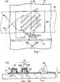
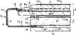
Fig. 1 shows the liquid-crystal apparatus 1 of present embodiment.This liquid-crystal apparatus 1 is to form by non-display surface one side (the following side of Fig. 1) that is connected to FPC (flexible base, board) 3a and FPC3b on the liquid crystal panel 2, light conductor 4 is installed in liquid crystal panel 2 again.With liquid crystal panel 2 opposite sides control basal plate 5 is set at light conductor 4.This control basal plate 5 is according to circumstances as constituting will usually using of liquid-crystal apparatus, or as constituting will usually using of electronic installation that liquid-crystal apparatus is installed.FPC3a is used for being connected with control basal plate 5 electric conductivity ground with liquid crystal panel 2 under the situation of present embodiment with FPC3b.
Liquid crystal panel 2 has a pair of substrate 7a and the 7b that is fitted mutually by the encapsulant 6 of ring-type.On the surface of the part of stretching out from the 2nd substrate 7b in the 1st substrate 7a, utilize AFC (anisotropic conductive film) 9 that liquid crystal drive IC8a are installed.In addition, on the surface (downside surface of Fig. 1) of the part of stretching out from the 1st substrate 7a in the 2nd substrate 7b, utilize AFC9 that liquid crystal drive IC8b is installed.
The liquid-crystal apparatus of present embodiment has been to use the liquid-crystal apparatus of TFD as the active matrix mode of on-off element, and a certain side of the 1st substrate 7a and the 2nd substrate 7b is a device substrate, and the opposing party is a counter substrate.In the present embodiment, the 1st substrate 7a is decided to be device substrate, the 2nd substrate 7b is decided to be counter substrate.
As shown in Figure 2, as forming pixel electrode 66 on the inside surface of the 1st substrate 7a of device substrate, paste polaroid 12a on its outer surface.In addition, on as the inside surface of the 2nd substrate 7b of counter substrate, form data line 52, paste polaroid 12b on its outer surface.And, in the gap that is surrounded by the 1st substrate 7a, the 2nd substrate 7b and encapsulant 6, be to enclose liquid crystal L in the so-called cell gap.
Though not shown in Fig. 2, above-mentioned various optical parameters in addition are set on the 1st substrate 7a and the 2nd substrate 7b as required.The alignment films of the orientation alignment usefulness that makes liquid crystal L for example, is set on the inside surface of each substrate.These alignment films are for example by forming by baking after having applied polyimide solution.Utilize milled processed that the main chain of the polymkeric substance of this polyimide is extended towards the direction of regulation, we can say by the bearing of trend travel direction coordination of the liquid crystal molecule in the liquid crystal L in the inclosure cell gap along alignment films.
In addition, carrying out under the colored situation about showing, on the counter substrate of the part relative, form the color filter of R (red), G (green), each primary colors of B (indigo plant), on not relative zone, form the Bk black matrix" of (deceiving) with pixel electrode with predetermined arrangement with the pixel electrode that is forming on the device substrate.Moreover, for the smoothing on the surface of color filter and black matrix" with protect, covered the smoothing layer.On above-mentioned smoothing layer, form the opposite electrode that is arranged on the counter substrate side.
Fig. 3 schematically shows the electric structure of liquid crystal panel 2.Such as shown, on liquid crystal panel 2, go up formation multi-strip scanning line 51 at line direction (directions X), moreover, go up many data lines 52 of formation at column direction (Y direction), on each point of crossing of sweep trace 51 and data line 52, form pixel 53.Each pixel 53 is by forming with liquid crystal layer 54 and being connected in series of TFD (thin film diode) 56.
Each sweep trace 51 is driven by scan line drive circuit 57, and in addition, each data line 52 is driven by data line drive circuit 58.Under the situation of present embodiment, scan line drive circuit 57 is included in the liquid crystal drive of Fig. 1 with among the IC8a, and data line drive circuit 58 is included in the liquid crystal drive of Fig. 1 with among the IC8b.
In Fig. 3, sweep trace 51 and TFD56 are formed on the inside surface of the device substrate 7a of Fig. 2, and in addition, the pixel electrode 66 that forms on the inside surface of device substrate 7a is connected with sweep trace 51.On the other hand, in Fig. 3, data line 52 electrode as strip on the inside surface of the counter substrate 7b of Fig. 2 is formed.Mutually applying device substrate 7a and counter substrate 7b make the pixel electrode 66 of 1 row part and the position that 1 data line 52 becomes opposite one another concern.Therefore, liquid crystal layer 54 just is made of data line 52, pixel electrode 66 and the liquid crystal L that is clamped in therebetween.
Data line 52 is for example formed by the such transparent conductive material of ITO (indium tin oxide).In addition, pixel electrode 66 is formed by the such reflective material of Al (aluminium).Have again, in Fig. 3, TFD56 is connected to sweep trace 51 1 sides, liquid crystal layer 54 is connected to data line 52 1 sides, but also can be opposite with it, TFD56 is connected to data line 52 1 sides, liquid crystal layer 54 is connected to sweep trace 51 1 sides.
Secondly, Fig. 4 shows the structure of 1 pixel portion among the device substrate 7a.Particularly, Fig. 4 (a) illustrates the planar structure of the structure of its 1 pixel portion, and Fig. 4 (b) shows along the cross-section structure of the A-A line of Fig. 4 (a).In these figure, TFD56 partly is made of the 1TFD56a that forms on the lip-deep dielectric film 61 of device substrate 7a in film forming and 2 such TFD of 2TFD56b.For example use tantalum oxide (Ta
2O
5) form dielectric film 61 with the thickness of about 50~200mm.
TFD56a and 56b respectively by the 1st metal film 62, on the surface of the 1st metal film 62, form and constitute as the oxide film 63 of the effect of insulator and the 2nd metal film 64a and the 64b that on the surface of oxide film 63, forms disconnected from each otherly.Oxide film 63 is for example by carrying out the tantalum oxide (Ta that oxidation forms with anodizing to the surface of the 1st metal film 62
2O
5) constitute.Have again, also simultaneously oxidized as the surface of the part on the basis of sweep trace 51 when the 1st metal film 62 is carried out anodic oxidation, the same oxide film that constitutes by tantalum oxide that forms.
Select its comparatively desirable value according to the purposes of oxide film 63, for example about 10~35nm.This thickness is and uses the situation of 1 TFD to be in a ratio of the thickness of half for 1 pixel.In addition, as the liquid that changes into that uses in the anodic oxidation, be not limited to the specific liquid that changes into, but can use for example aqueous citric acid solution of 0.01~0.1 percentage by weight.
For example, the reflective material of using the film technique of sputtering method etc. that Al (aluminium) is waited has been carried out after the film forming, utilizes photoetching and lithographic technique to carry out composition, final thickness with about 50~300nm forms the 2nd metal film 64a and 64b.One side's the 2nd metal film 64a directly becomes sweep trace 51, and the opposing party's the 2nd metal film 64b is connected with pixel electrode 66.
At this, if from sweep trace 51 sides, then 1TFD56a adopt in order the 2nd metal film 64a/ oxide film 63/ the 1st metal film 62 stepped construction, be the sandwich construction of metal/insulator/metal, therefore, its I-E characteristic is non-linear on positive and negative twocouese.On the other hand, if from sweep trace 51 sides, then 2TFD56b adopts the stepped construction of the 1st metal film 62/ oxide film 63/ the 2nd metal film 64b in order, has the I-E characteristic opposite with 1TFD56a.Thereby TFD56 becomes makes 2 elements be the form that is connected in series on the contrary mutually, therefore, compares with the situation of using 1 element, and the nonlinear characteristic of current-voltage is symmetry on positive and negative twocouese.
The 1st metal film 62 is for example formed by tantalum monomer, tantalum alloy etc.In addition, the thickness of the 1st metal film 62 is selected suitable value according to the purposes of TFD56, usually about 100~500nm.Have again,, in the tantalum of major component, add for example element that in the periodic law table, belongs to the 6th~the 8th family of tungsten, chromium, molybdenum, rhenium, yttrium, lanthanum, dysprosium etc. using under the situation of tantalum alloy as the 1st metal film 62.At this moment, as adding element, tungsten is comparatively desirable, wishes that it contains proportional for example is 0.1~6 percentage by weight.
Wherein, the matrix 17a of composed component substrate 7a is for example formed by quartz, glass, plastics etc. with the matrix 17b (with reference to Fig. 2) that constitutes counter substrate 7b.At this, under the situation of simple reflection-type, the matrix 17a of device substrate is that transparent this point is not a necessary condition, but under the situation about using as reflection-type and transmission-type as present embodiment, the matrix 17a of device substrate is that transparent this point is a necessary condition.
In addition, dielectric film 61 this point are set and are based on following reason on the surface of device substrate 7a.That is, the 1st, be in order not peel off from substrate because of the thermal treatment after the deposit of the 2nd metal film 64a and 64b makes the 1st metal film 62.In addition, the 2nd, be in order not make in diffusion of contaminants to the 1 metal film 62.Thereby, if these aspects do not become problem, then can omit dielectric film 61.
Have again, TFD56 is the example as 2 terminal type nonlinear elements, in addition, also can use the element of such employing diode element structure such as MSI (metal semi-insulator) or with reverse manner be connected in series or the be connected in parallel element of structure of these elements.Moreover, under the situation that there is no need strictly make I-E characteristic be symmetry on the positive and negative twocouese, can only utilize 1 element to constitute TFD.
In Fig. 4, the pixel electrode 66 that forms with the shape that prolongs from the 2nd metal film 64b is formed by the big metal film of reflectivity of Al (aluminium) etc.In addition, as shown in Fig. 4 (a), in pixel electrode 66, be arranged on the slot-shaped peristome 67 of vergence direction upper shed.When this liquid-crystal apparatus played the function of transmission-type, the light by these peristomes 67 entered in the liquid crystal layer 54 (with reference to Fig. 3).Have again, wish small fluctuating is set in pixel electrode 66, so that reflection light diffusing.
In liquid crystal panel 2 (with reference to Fig. 1), under the state at the certain interval of mutual maintenance, paste device substrate 7a and counter substrate 7b, in this gap, enclose liquid crystal L.(with reference to Fig. 2).And the visual characteristic of consideration liquid crystal panel under the situation of device substrate 7a, is used arrow R in Fig. 4 (a)
ASetting makes liquid crystal L have the grinding direction that orientation is used on the direction that illustrates, and under the situation of counter substrate 7b, is using arrow R
BSetting on the direction that illustrates makes liquid crystal L have the grinding direction that orientation is used.That is, the grinding direction in the orientation orientation of the liquid crystal molecule when determining not apply voltage, if having an X-rayed from counter substrate 7b one side when pasting the state of two substrates, then the counter substrate 7b of side in front of being arranged in is the direction R towards 45 ° of left oblique uppers
B, be arranged in the device substrate 7a of rear side, be the oblique direction R of 45 ° of belows towards a left side
AThereby, the slit direction of the peristome 67 among the device substrate 7a and grinding direction R
AAs one man form.
Have again, because in general milled processed is to be undertaken by the duck's down cloth that is wound on the cylinder in friction on the certain orientation, so the undesirable states of affairs such as static or various dusts take place in manufacturing process easily.In the present embodiment, because the direct of travel of duck's down cloth is consistent with the slit direction of peristome 67 in milled processed, so can reduce the influence because of the generation of the step difference of pixel electrode 66, its result can suppress the generation of static or the generation of various dusts.
Have again, in the above description, be decided to be identical with 64b with the composition of pixel electrode 66 the 2nd metal film 64a, but also can utilize composition to form the such non-reflective metal of chromium, titanium, molybdenum, utilize composition to form such reflective metal such as Al thereafter as pixel electrode 66 as the 2nd metal film 64a and 64b.
But, by pixel electrode 66 and the direction of an electric field that the data line 52 relative with it takes place, as shown in Figure 5, beyond peristome 67, become vertical direction with respect to two substrates, therefore, its intensity also is uniform.Different therewith, owing in peristome 67, there is not electrode, only be owing to electric field just takes place from the sewing of openend of pixel electrode 66.Therefore, near the electric field intensity peristome 67 dies down greatly with the distance change from openend, is not uniform.The point place that the marginal end portion that means in pixel electrode 66 peristome 67 that forms conversely speaking, is equidistant point, promptly be shown in broken lines in Fig. 6 (a), electric field about equally.
On the other hand, owing to the grinding direction of the device substrate 7a that has formed pixel electrode 66 is consistent with the slit direction of the peristome 67 that forms at this place, so when not applying voltage, carry out orientation abreast along the marginal end portion of peristome 67 at the liquid crystal molecule M of device substrate 7a one side.Thereby, between pixel electrode 66 and data line 52, taken place under the situation of potential difference (PD), particularly under the situation that this potential difference (PD) is little, an end and other end place at liquid crystal molecule M, electric field intensity equates, therefore, the liquid crystal molecule M that is positioned at peristome 67 be positioned at zone that electrode exists, help the liquid crystal molecule in the zone that shows similarly to tilt when promptly playing the function of reflection-type.Therefore, because the light by peristome 67 and the catoptrical optical direction that is reflected by pixel electrode 66 are mutually about equally, so can reduce display quality poor of transmission-type and reflection-type.
As mentioned above, the slit direction of wishing peristome 67 is with to grind direction consistent mutually, if but both be in ± 15 ° with in the interior angular range, can think that then the difference of above-mentioned display quality is unobstructive degree practical.
Have, under the inconsistent situation of slit direction of grinding direction and peristome 67, as shown in Fig. 6 (b), the liquid crystal molecule M that is positioned at peristome 67 carries out orientation on the direction of intersecting with the marginal end portion of peristome 67 when not applying voltage again.Therefore, even between pixel electrode 66 and data line 52, taken place under the situation of potential difference (PD), particularly under the situation that this potential difference (PD) is little, electric field intensity at the end of liquid crystal molecule M and the other end is also unequal, therefore, do not help the liquid crystal molecule in the zone that shows similarly to tilt when using with being positioned at as reflection-type.Its result, since different at light with optical direction in the reflected light that is reflected by pixel electrode 66 by peristome 67, so creating a difference aspect the display quality of transmission-type and reflection-type.
Secondly, the width and the area of research peristome 67 of formation in pixel electrode 66.
In general, at the liquid crystal of enclosing between a pair of substrate is under the situation of TN (twisted-nematic) type, substrate is spaced apart several microns, at this moment, for example if normal white mode, even then from about 1.5 microns some place, end in the zone of the electrode crossing of two substrates, if apply voltage, then the electric field effects that also spills because of the end from the periphery of electrode is deceived demonstration.
According to this point, if the width of the peristome 67 in slit is 1.5 microns a multiple, promptly about below 3 microns in Fig. 4 (a), then because the electric field that spills from the both side ends of peristome 67, the existence zone of the liquid crystal molecule of this peristome 67 and electrode similarly tilts.If the width W with slot-shaped peristome 67 is decided to be more than 3 microns conversely speaking,, then in reflection-type might as well, in transmission-type might as well, all in pixel electrode 66, form the dead space that liquid crystal molecule M does not tilt because of electric field.Thereby, can think that the width W of wishing peristome 67 is about below 3 microns.
Under the width W with peristome 67 is decided to be situation below 3 microns,, then can imagine enough light quantities that can not obtain being enough to playing the function of transmission-type if because the cause of the size of pixel electrode 66 is not provided with a plurality of peristomes 67.On the contrary, increase its total area,,, pretend the display frame deepening when using into reflection-type because correspondingly reflection light quantity reduces though then increase as the transmission light quantity of the situation of transmission-type if a plurality of peristomes 67 are set.According to experiment, be set at area under 10~25% the situation of area of pixel electrode 66 peristome 67, can carry out as can be known that transmission-type shows and the reflection-type demonstration with good balance.Have again, the area of said here pixel electrode 66, strictly speaking, refer to pixel electrode 66 and data line 52 the intersection region, be not by the area of effective viewing area of black matrix" shading.
Turn back to Fig. 1, on as the extension of the device substrate 7a of device substrate, form a plurality of terminal 13a.With as the surface of the device substrate 7a in the relative zone of the counter substrate 7b of counter substrate on form these terminals when forming pixel electrode 66 simultaneously.In addition, on the extension of counter substrate 7b, also form a plurality of terminal 13b.Form these terminals when on the surface of the counter substrate 7b in the zone relative, forming data line 52 simultaneously with device substrate 7a.
Make FPC3a and FPC3b by on the flexbile base that constitutes at material the metal film figure being formed desirable graphics shape by polyimide etc.A plurality of terminals 22 are set on the marginal end portion of FPC3b, use such conductive adhesive key element such as ACF with these terminal electric conductivity be connected on the terminal 13b of the 2nd substrate 7b.
The a plurality of terminals 23 that form on another marginal end portion of FPC3b are connected with the terminal that is provided with on the suitable position of control basal plate 5 (not shown).
On the other hand, about FPC3a, on the back side one side (downside of Fig. 1) of the marginal end portion of liquid crystal panel 2 one sides, a plurality of panel side terminals 14 are set, with the surface (upper side of Fig. 1) of the marginal end portion of liquid crystal panel 2 opposite sides on a plurality of control basal plate side terminals 16 are set.In addition, form suitable wiring figure 18 in the wide scope on the surface of FPC3a, this wiring figure 18 directly is connected with control basal plate side terminal 16 a side, is connected at the panel side terminal 14 of the opposing party's via through holes 19 with the back side one side.
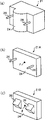
In addition, the back side of FPC3a, promptly with the face of wiring figure 18 opposite sides on, with 1 row a plurality of LED (light emitting diode) 21 as the light-emitting component of formation lighting device have been installed with the spaced-apart synergistically proper spacing of light conductor 4.Be used for the wiring of these LED21, for example via through holes is connected with control basal plate side terminal 16.LED21 has the pin 26 of locating device that for example conduct as shown in Fig. 7 (a) is positioned at the both sides of light-emitting area 24, these light-emitting areas 24 and pin 26 in Fig. 1 towards with the direction shown in the arrow B, be the reverse direction of FPC3a.
Utilize to paste wait and to disperse sheet 27 and be installed on the surface of liquid crystal panel 2 sides of light conductor 4, utilize to paste to wait reflector plate 28 is installed on light conductor 4 and surfaces liquid crystal panel 2 opposite sides.Reflector plate 28 is taken into the direction reflection of face 4a towards liquid crystal panel 2 from the light of light conductor 4.In addition, disperse sheet 27 disperse like this from light conductor 4 towards liquid crystal panel 2 penetrate light, make it become uniform intensity in the plane.
The light of light conductor 4 be taken into be provided with on the face 4a be installed in FPC3a on the holding of the corresponding number of the number of LED21 with recess 29, hold both sides with recess 29 at these and be provided with and locate usefulness recess 31.These location do not concern form that can have the size of loosely inserting pin 26 and position this pin 26 forms with recess 31 on the light-emitting area 24 that is installed in the LED21 on the FPC3a.
As shown in Figure 2, light conductor 4 is clamped the non-display surface side that the padded coaming 32 that is formed by plastics etc. is installed in liquid crystal panel 2.In addition, the face with the reflector plate 28 that light conductor 4 has been installed relatively disposes control basal plate 5.This control basal plate 5 is installed on the non-demonstration side surface of light conductor 4 as the key element that constitutes liquid-crystal apparatus 1 sometimes, perhaps, the situation that becomes the inscape that constitutes the electronic installation that uses this liquid-crystal apparatus 1 is arranged also.Formation obtains the terminal that is connected usefulness 33 with external circuit on the marginal end portion of control basal plate 5.
In assembly drawing 1, during with each component part of the liquid-crystal apparatus shown in the decomposing state, as shown in Figure 2, utilize ACF34 that the marginal end portion of liquid crystal panel 2 sides of FPC3a is bonded on the extension of the 1st substrate 7a.Utilize this bonding, utilize the conducting particles electric conductivity ground in the ACF34 to connect the terminal 13a of the 1st substrate 7a and the terminal 14 of FPC3a., along the light of light conductor 4 be taken into face 4a crooked FPC3a, under this case of bending the marginal end portion of FPC3a overlapped onto on the marginal end portion of control basal plate 5 thereafter.Then, to the terminal 33 of control basal plate 5 sides, or utilize other electrically conductive connection method to connect terminal 16 solderings of FPC3a side.
Connecting and as mentioned above during crooked FPC3a in order to conduct electricity, the light that the light-emitting area 24 (with reference to Fig. 7 (a)) that is installed in lip-deep a plurality of LED21 of FPC3a is accommodated in light conductor 4 is taken into face 4a and goes up holding with in the recess 29 of forming, moreover the pin 26 that is provided with on the light-emitting area 24 of LED21 is fitted to the location with in the recess 31.Utilize above operation, as shown in Figure 2, the light that LED21 is installed in light conductor 4 is taken among the face 4a, constitutes liquid crystal panel 2 is supplied with the lighting device that light is used.The FPC3b of the opposing party shown in Fig. 1 too, formed terminal 23 marginal end portion electric conductivity be connected on the terminal of the control basal plate side that forms on the suitable position of control basal plate 5.
Liquid-crystal apparatus 1 about above formation, in Fig. 2, if LED21 is luminous, then the light that penetrates from light-emitting area 24 is imported into the light conductor 4, sheet 28 reflection that is reflected of this light that is imported into, direction towards liquid crystal panel 2 is advanced, and is dispersed sheet 27 at quilt and diverges to supply liquid crystal panel 2 under the state that planar becomes uniform intensity.The light that is supplied to has passed through the component of the polaroid 12a on leaded light side and has supplied with liquid crystal layer, moreover, utilize variation according to the voltage that between pixel electrode 66 and data line 52, is applied in to Be Controlled in each pixel the liquid crystal that is orientated in each pixel, modulate, moreover, the polaroid 12b that shows side by this light modulated is led to externally shows picture.
As mentioned above, in the liquid-crystal apparatus 1 of present embodiment, utilize the FPC3a that is connected carry out the electric conductivity between liquid crystal panel 2 and the control basal plate 5 to support LED21, eliminated the substrate of the special use that is used to support LED21, therefore, can be used in the supporting construction that supports LED21 simplifies very much.Therefore, the cost that can realize liquid-crystal apparatus reduces and miniaturization.
In addition, utilize the chimeric of pin 26 and recess 31, all the time LED21 is taken into face 4a with respect to the light of light conductor 4 and is positioned on certain position, moreover, when the use of liquid-crystal apparatus 1, prevent to be offset with respect to light conductor 4 occurrence positions.Thereby, in each goods,, can stably make the uniform liquid-crystal apparatus 1 of a plurality of display characteristics aspect the lightness of the demonstration of liquid crystal panel 2 discreteness not taking place.
In addition, in the present embodiment, LED21 is installed on the face identical with the terminal 14 of liquid crystal panel 2 sides of FPC3a, wiring figure 18 via through holes 19 by FPC3a are connected with this terminal 14, and it is arranged on the face of an opposite side with LED21.Thereby, can freely carry out graphic designs and not hinder LED21 wiring figure 18.
(the 2nd embodiment)
Fig. 8 shows another embodiment of liquid-crystal apparatus of the present invention.In this embodiment, the member identical with the situation of the embodiment shown in Fig. 1 illustrates with identical symbol, omits the explanation about these members.In addition, the structure of unshowned part is identical with the embodiment shown in Fig. 1 in Fig. 8.
Present embodiment is with the different aspect of the embodiment shown in Fig. 1, at the face identical with the face that LED21 has been installed, promptly formed the whole of the liquid crystal panel side terminal 14, control basal plate side terminal 16 and the wiring figure 18 that are provided with under the situation at Fig. 8 on below figure on the FPC3c as flexible base, board.At this moment since can not be on identical position laying-out and wiring figure 18 and LED21, so form wiring figure 18 in the mode that gets around LED21.
(the 3rd embodiment)
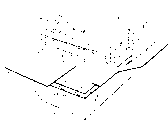
Fig. 9 shows the major part of the another embodiment of liquid-crystal apparatus of the present invention.In this embodiment, the member identical with the situation of the embodiment shown in Fig. 1 and Fig. 2 illustrates with identical symbol, omits the explanation about these members.In addition, the structure of unshowned part is identical with the embodiment shown in Fig. 1 and Fig. 2 in Fig. 9.
Present embodiment is with the different aspect of the embodiment shown in Fig. 2, the light that forms light conductor 4A with the curved shape towards the relative direction of liquid crystal panel 2 is taken into face 4a, the light-emitting area 24 of the LED21 that is supported by FPC3a electric conductivity be connected under the state of terminal 33 of control basal plate 5, be taken into face 4a with this light that is bent and relatively dispose.
According to present embodiment, can between light conductor 4A and FPC3a, form wide space R, owing to this space R can be used to hold other electronic unit of the chip capacitor that is installed on the FPC3a etc., so be comparatively desirable.
(the 4th embodiment)
Figure 10 shows the major part of the another embodiment of liquid-crystal apparatus of the present invention.In this embodiment, the member identical with the situation of the embodiment shown in Fig. 1 and Fig. 2 illustrates with identical symbol, omits the explanation about these members.In addition, the structure of unshowned part is identical with the embodiment shown in Fig. 1 and Fig. 2 in Figure 10.
Present embodiment is with the different aspect of the embodiment shown in Fig. 2, the light-emitting area 24 of LED21 becomes the side towards the installed surface of FPC3a, carry out under the state that is connected of electric conductivity with the terminal 33 of control basal plate 5 at FPC3a, the light-emitting area 24 of its side is taken into face 4a with the light of light conductor 4 and relatively disposes.
According to present embodiment, can between light conductor 4 and FPC3a, form wide space R, owing to this space R can be used to hold other electronic unit of the chip capacitor that is installed on the FPC3a etc., so be comparatively desirable.
(the 5th embodiment)
Fig. 7 (b) shows the variation 21A as the LED of light-emitting component.This LED21A is becoming on this point of plane different with the LED21 shown in Fig. 7 (a) about the light-emitting area 24 around the luminous point F.
(the 6th embodiment)
Fig. 7 (c) shows another variation 21B as the LED of light-emitting component.This LED21B replaces pin 26 different with the LED21 shown in Fig. 7 (a) on as the locating device this point in the projection 36 that becomes plane this point and use triangle column about the light-emitting area 24 around the luminous point F.
(embodiment of electronic installation)
Figure 11 shows 1 embodiment of liquid-crystal apparatus of the present invention as the situation of the display device use of various electronic installations.Comprise at the electronic installation shown in this: display message output source 100; Display message treatment circuit 101; Power circuit 102; Timing sequencer 103; And liquid-crystal apparatus 104.In addition, liquid-crystal apparatus 104 has liquid crystal panel 105 and driving circuit 106.Liquid-crystal apparatus 104 can use the liquid-crystal apparatus 1 shown in Fig. 1.Liquid crystal panel 105 can use the liquid crystal panel 2 shown in Fig. 1.
Display message output source 100 comprises: ROM (ROM (read-only memory)); The storer of RAM (random access memory) etc.; The storage unit of various dishes etc.; And data image signal carried out tuned circuit etc. tuning and output, its supplies with display message treatment circuit 101 according to the various clock signals from timing sequencer 103 with the display message such as picture signal of predetermined format.
Display message treatment circuit 101 possesses: go here and there translation circuit in the lump; Amplification, circuit for reversing; Deflection circuit; Gamma (γ) correcting circuit; And well-known various treatment circuits such as clamp circuit, its carries out the processing of the display message of being imported, and this picture signal is supplied with driving circuit 106 with clock signal clk.Driving circuit 106 is the circuit that the scan line drive circuit among Fig. 3 57, data line drive circuit 58, check circuit etc. carried out general name.In addition, power circuit 102 is supplied with each inscape with predetermined power supply.
Figure 12 shows the personal computer as the mobile model of an embodiment of electronic installation of the present invention.Have body 112 and the liquid crystal display 113 that has keyboard 111 at the personal computer shown in this 110.Liquid crystal display 113 comprises the liquid-crystal apparatus 1 shown in Fig. 1 and constitutes.Figure 13 shows the portable telephone as another embodiment of electronic installation of the present invention.Have a plurality of action buttons 121 and liquid-crystal apparatus 1 at the portable telephone shown in this 120.
Because the liquid-crystal apparatus 1 that uses among the embodiment of Figure 12 and Figure 13 is the liquid-crystal apparatus of the semi-transparent semi that illustrates with Fig. 1 relatedly, even so computing machine or portable telephone are placed the inadequate place of exterior light, by making the lighting device that constitutes by LED21 and light conductor 4, so-called back of the body irradiation source point bright, also can have any obstruction ground and do not show.
In addition, in the liquid-crystal apparatus 1 of Fig. 1, utilize the FPC3a that is connected carry out the electric conductivity between liquid crystal panel 2 and the control basal plate 5 to support LED21, eliminated the substrate that supports the special use that LED21 uses, therefore, the supporting construction that LED21 is used the very simplification that becomes.Therefore, can form small-sized liquid-crystal apparatus 1, in Figure 12, in liquid crystal display 113 that this liquid-crystal apparatus 1 is packed into, can be with the frame of liquid crystal display 113 part, be that so-called frame district forms narrowlyer.In addition, about the portable telephone 120 of Figure 13, by the miniaturization of liquid-crystal apparatus 1, even under the situation of the profile that reduces portable telephone, the big display part of also packing into.
In addition, in Fig. 2, utilize the chimeric of pin 26 and recess 31, all the time LED21 being taken into face 4a with respect to the light of light conductor 4 is positioned on certain position, moreover, when the use of liquid-crystal apparatus 1, prevent to be offset with respect to light conductor 4 occurrence positions, therefore, the discreteness of elimination aspect the lightness of the demonstration of liquid crystal panel 2 in each goods.Therefore, in each goods,, can obtain uniform display characteristic also not having discreteness aspect the lightness of the display frame of the portable telephone 120 of the lightness of the display frame of the computing machine of Figure 12 and Figure 13.
(other embodiment)
More than enumerate preferred embodiment the present invention has been described, but the present invention is not limited to this embodiment, can in the scope of claim record, do various changes.
For example, among the embodiment shown in Figure 1, apply the present invention in semi-transparent semi, to have used the liquid-crystal apparatus of the active matrix mode of TFD, the present invention also can be applicable to liquid-crystal apparatus, the transmission-type of liquid-crystal apparatus, for example reflection-type of other variety of way liquid-crystal apparatus, used the active matrix mode of the on-off element beyond the TFD liquid-crystal apparatus, do not use the liquid-crystal apparatus etc. of the passive matrix mode of on-off element.
As discussed above, according to liquid-crystal apparatus of the present invention, on the flexible base, board that is connected on the substrate of holding liquid crystal, light-emitting component is installed, because this flexible base, board is the substrate that is used for for certain electrical wiring of liquid crystal, it or not the substrate that light-emitting component is installed to the special use on the light conductor, so the supporting construction of light-emitting component is simplified very much, therefore, can realize that the cost of liquid-crystal apparatus reduces and miniaturization.