EP1156891B1 - Low profile acoustic sensor array and sensors with pleated transmission lines and related methods - Google Patents
Low profile acoustic sensor array and sensors with pleated transmission lines and related methods Download PDFInfo
- Publication number
- EP1156891B1 EP1156891B1 EP00912045A EP00912045A EP1156891B1 EP 1156891 B1 EP1156891 B1 EP 1156891B1 EP 00912045 A EP00912045 A EP 00912045A EP 00912045 A EP00912045 A EP 00912045A EP 1156891 B1 EP1156891 B1 EP 1156891B1
- Authority
- EP
- European Patent Office
- Prior art keywords
- sensor
- acoustic
- acoustic sensor
- layer
- sensor element
- Prior art date
- Legal status (The legal status is an assumption and is not a legal conclusion. Google has not performed a legal analysis and makes no representation as to the accuracy of the status listed.)
- Expired - Lifetime
Links
- 238000000034 method Methods 0.000 title claims abstract description 21
- 230000005540 biological transmission Effects 0.000 title claims description 49
- 239000010410 layer Substances 0.000 claims description 244
- 239000002033 PVDF binder Substances 0.000 claims description 119
- 229920002981 polyvinylidene fluoride Polymers 0.000 claims description 119
- 239000000463 material Substances 0.000 claims description 70
- 230000004044 response Effects 0.000 claims description 45
- 239000012792 core layer Substances 0.000 claims description 17
- 238000003491 array Methods 0.000 claims description 12
- 239000000853 adhesive Substances 0.000 claims description 8
- 230000001070 adhesive effect Effects 0.000 claims description 8
- 239000011149 active material Substances 0.000 claims description 7
- 238000006073 displacement reaction Methods 0.000 claims description 5
- 230000008859 change Effects 0.000 claims description 4
- 210000004351 coronary vessel Anatomy 0.000 claims description 4
- 238000004891 communication Methods 0.000 claims description 3
- 238000002955 isolation Methods 0.000 claims 1
- 239000011162 core material Substances 0.000 description 63
- 239000010408 film Substances 0.000 description 51
- 230000006835 compression Effects 0.000 description 18
- 238000007906 compression Methods 0.000 description 18
- 239000003351 stiffener Substances 0.000 description 16
- 210000003491 skin Anatomy 0.000 description 10
- 238000001514 detection method Methods 0.000 description 9
- 229920001084 poly(chloroprene) Polymers 0.000 description 9
- 238000004519 manufacturing process Methods 0.000 description 7
- 230000007935 neutral effect Effects 0.000 description 7
- 230000017531 blood circulation Effects 0.000 description 6
- 239000003973 paint Substances 0.000 description 6
- 229920002799 BoPET Polymers 0.000 description 5
- 210000000038 chest Anatomy 0.000 description 5
- 230000005284 excitation Effects 0.000 description 5
- 230000036961 partial effect Effects 0.000 description 5
- 229920000728 polyester Polymers 0.000 description 5
- 238000000151 deposition Methods 0.000 description 4
- 229920006267 polyester film Polymers 0.000 description 4
- -1 polyethylene Chemical group 0.000 description 4
- 230000002441 reversible effect Effects 0.000 description 4
- 239000005041 Mylar™ Substances 0.000 description 3
- 230000004913 activation Effects 0.000 description 3
- 239000012790 adhesive layer Substances 0.000 description 3
- 238000000576 coating method Methods 0.000 description 3
- 208000029078 coronary artery disease Diseases 0.000 description 3
- 230000008878 coupling Effects 0.000 description 3
- 238000010168 coupling process Methods 0.000 description 3
- 238000005859 coupling reaction Methods 0.000 description 3
- 238000010586 diagram Methods 0.000 description 3
- 230000003601 intercostal effect Effects 0.000 description 3
- 238000012986 modification Methods 0.000 description 3
- 230000004048 modification Effects 0.000 description 3
- 230000035945 sensitivity Effects 0.000 description 3
- 238000000926 separation method Methods 0.000 description 3
- 230000008054 signal transmission Effects 0.000 description 3
- 238000013519 translation Methods 0.000 description 3
- 239000004698 Polyethylene Chemical group 0.000 description 2
- BQCADISMDOOEFD-UHFFFAOYSA-N Silver Chemical compound [Ag] BQCADISMDOOEFD-UHFFFAOYSA-N 0.000 description 2
- 230000000747 cardiac effect Effects 0.000 description 2
- 239000004020 conductor Substances 0.000 description 2
- 238000002788 crimping Methods 0.000 description 2
- 230000000694 effects Effects 0.000 description 2
- 238000013017 mechanical damping Methods 0.000 description 2
- 229920000573 polyethylene Chemical group 0.000 description 2
- 229910052709 silver Inorganic materials 0.000 description 2
- 239000004332 silver Substances 0.000 description 2
- 239000010409 thin film Substances 0.000 description 2
- MIZLGWKEZAPEFJ-UHFFFAOYSA-N 1,1,2-trifluoroethene Chemical group FC=C(F)F MIZLGWKEZAPEFJ-UHFFFAOYSA-N 0.000 description 1
- 229910001080 W alloy Inorganic materials 0.000 description 1
- 230000002159 abnormal effect Effects 0.000 description 1
- 230000003213 activating effect Effects 0.000 description 1
- 230000002411 adverse Effects 0.000 description 1
- 238000004458 analytical method Methods 0.000 description 1
- 230000004888 barrier function Effects 0.000 description 1
- 230000009286 beneficial effect Effects 0.000 description 1
- 230000008901 benefit Effects 0.000 description 1
- 239000008280 blood Substances 0.000 description 1
- 210000004369 blood Anatomy 0.000 description 1
- 238000013155 cardiography Methods 0.000 description 1
- 239000011248 coating agent Substances 0.000 description 1
- 238000004590 computer program Methods 0.000 description 1
- 238000010276 construction Methods 0.000 description 1
- 229920001577 copolymer Polymers 0.000 description 1
- 239000006071 cream Substances 0.000 description 1
- 238000005520 cutting process Methods 0.000 description 1
- 230000007812 deficiency Effects 0.000 description 1
- 238000003745 diagnosis Methods 0.000 description 1
- 238000007598 dipping method Methods 0.000 description 1
- 230000009977 dual effect Effects 0.000 description 1
- 238000005566 electron beam evaporation Methods 0.000 description 1
- 230000007613 environmental effect Effects 0.000 description 1
- 210000002615 epidermis Anatomy 0.000 description 1
- 235000012438 extruded product Nutrition 0.000 description 1
- 239000011888 foil Substances 0.000 description 1
- PCHJSUWPFVWCPO-UHFFFAOYSA-N gold Chemical compound [Au] PCHJSUWPFVWCPO-UHFFFAOYSA-N 0.000 description 1
- 229910052737 gold Inorganic materials 0.000 description 1
- 239000010931 gold Substances 0.000 description 1
- 230000005484 gravity Effects 0.000 description 1
- 208000019622 heart disease Diseases 0.000 description 1
- 238000010438 heat treatment Methods 0.000 description 1
- 229910001385 heavy metal Inorganic materials 0.000 description 1
- 229920001903 high density polyethylene Chemical group 0.000 description 1
- 239000004700 high-density polyethylene Chemical group 0.000 description 1
- 238000003384 imaging method Methods 0.000 description 1
- 230000002401 inhibitory effect Effects 0.000 description 1
- 239000012212 insulator Substances 0.000 description 1
- 230000003993 interaction Effects 0.000 description 1
- 229920000126 latex Chemical group 0.000 description 1
- 239000004816 latex Chemical group 0.000 description 1
- 230000003902 lesion Effects 0.000 description 1
- 230000000670 limiting effect Effects 0.000 description 1
- 238000005259 measurement Methods 0.000 description 1
- 229910052751 metal Inorganic materials 0.000 description 1
- 239000002184 metal Substances 0.000 description 1
- 239000011104 metalized film Substances 0.000 description 1
- 238000001465 metallisation Methods 0.000 description 1
- 239000000203 mixture Substances 0.000 description 1
- 150000002825 nitriles Chemical group 0.000 description 1
- 239000012811 non-conductive material Substances 0.000 description 1
- 238000004806 packaging method and process Methods 0.000 description 1
- 238000010422 painting Methods 0.000 description 1
- 230000010287 polarization Effects 0.000 description 1
- 229920000642 polymer Polymers 0.000 description 1
- 229920006254 polymer film Polymers 0.000 description 1
- 230000008569 process Effects 0.000 description 1
- 238000012545 processing Methods 0.000 description 1
- 230000001681 protective effect Effects 0.000 description 1
- 230000002829 reductive effect Effects 0.000 description 1
- 230000002787 reinforcement Effects 0.000 description 1
- 239000012858 resilient material Substances 0.000 description 1
- 230000001953 sensory effect Effects 0.000 description 1
- 238000004513 sizing Methods 0.000 description 1
- 238000010183 spectrum analysis Methods 0.000 description 1
- 238000005507 spraying Methods 0.000 description 1
- 238000004544 sputter deposition Methods 0.000 description 1
- 210000001562 sternum Anatomy 0.000 description 1
- 238000003860 storage Methods 0.000 description 1
- 230000000153 supplemental effect Effects 0.000 description 1
- 238000002207 thermal evaporation Methods 0.000 description 1
- 210000000115 thoracic cavity Anatomy 0.000 description 1
- 230000007704 transition Effects 0.000 description 1
Images


Classifications
-
- B—PERFORMING OPERATIONS; TRANSPORTING
- B06—GENERATING OR TRANSMITTING MECHANICAL VIBRATIONS IN GENERAL
- B06B—METHODS OR APPARATUS FOR GENERATING OR TRANSMITTING MECHANICAL VIBRATIONS OF INFRASONIC, SONIC, OR ULTRASONIC FREQUENCY, e.g. FOR PERFORMING MECHANICAL WORK IN GENERAL
- B06B1/00—Methods or apparatus for generating mechanical vibrations of infrasonic, sonic, or ultrasonic frequency
- B06B1/02—Methods or apparatus for generating mechanical vibrations of infrasonic, sonic, or ultrasonic frequency making use of electrical energy
- B06B1/06—Methods or apparatus for generating mechanical vibrations of infrasonic, sonic, or ultrasonic frequency making use of electrical energy operating with piezoelectric effect or with electrostriction
- B06B1/0688—Methods or apparatus for generating mechanical vibrations of infrasonic, sonic, or ultrasonic frequency making use of electrical energy operating with piezoelectric effect or with electrostriction with foil-type piezoelectric elements, e.g. PVDF
Definitions
- the present invention relates generally to disposable acoustic sensors for capturing sounds from within the human body.
- the acoustic sensors are particularly useful for non-invasive digital acoustic cardiography, phonography, and acoustic spectral analysis applications.
- sensors are configured on a patient's chest ( i . e ., contacting the external epidermal surface or skin) to generate an electrical signal in response to a detected acoustic wave.
- the detected acoustic wave signals are processed to identify features that indicate the condition of a patient's coronary arteries, specifically the presence or absence of lesions that limit the flow of blood through the coronaries.
- An essentially uniform display indicates normal blood flow, while a non-uniform display may indicate abnormal (turbulent) blood flow and/or the presence of an occlusion.
- the acoustic sensors are positioned over the chest cavity in an acoustic window as described in co-pending and co-assigned U.S. Patent No. 6,193,668, entitled, "Acoustic Sensor Array For Non-Invasive Detection of Coronary Artery Heart Disease .”
- the sensors are preferably configured over the intercostal space so as to reliably generate data signals corresponding to the blood flow of the patient during each phase of the cardiac cycle.
- the acoustic sensor is preferably designed to sense the flexing of a patient's external epidermal surface (skin) that is a result of the localized nature of the internal heart sounds.
- the sensor is also preferably easy to position on a patient and inexpensive such that it can be a single use device, which is disposable after use.
- the sensor is preferably configured to be conformal to the chest configuration of a patient (which varies patient to patient) and is also preferably configured to generate the electrical signal based on the flexure of the skin.
- poor correlation of signals from improper sensor positioning, array geometry, and/or sensor configurations can adversely affect the reliability and/or correlation of the detected acoustic signal.
- one potentially problematic sensor characteristic is that it can generate signals which are not representative of the interested acoustic wave associated with the blood flow of a patient, i. e., it can be responsive to extraneous acoustic waves and noise.
- acoustic sensors can have poor signal to noise ratio (SNR) in that they can be unduly sensitive to environmental noise (typically requiring a special, quiet room be used for acoustic applications) or can suffer from low sensitivity relative to its electrical floor.
- SNR signal to noise ratio
- Other sensors have other performance deficiencies such as inadequate sensitivity.
- many sensors are relatively complex configurations which can make them expensive to produce and difficult to apply clinically.
- U.S. Patent No. 5.885,222 An example of a conventional disposable acoustic pad sensor is illustrated in U.S. Patent No. 5.885,222.
- the sensor includes a plurality of layers of various materials connected at one end to a substantially rigid electrostatic shield and electrical connector.
- Another example of an acoustic sensor is shown in U.S. Patent No. 6,261,237.
- This sensor is a flexible thin-film sensor which includes a foot portion and a two-piece piezoelectric film support.
- Still other examples of acoustic sensors are described in U.S. Patents 5,365,937, and 5,807,268. These sensors employ an air gap and a frame which acts to stretch and hold a polymer film in tension.
- US-A-5 807 271 describes a sensor array according to the preamble of claim 1.
- a low profile acoustic sensory array which acts as a mechanical filter to minimize the sensor's signal activation or response to extraneous and/or undesired acoustic wavelengths or non-relevant acoustic wave components.
- Such a device is selectively responsive to short wavelengths that cause flexure through the thickness of the sensor, while resistant to longer acoustic wavelengths.
- the longer wavelengths are typically associated with compression waves in the body or in ambient noise within the examining room, and which can cause compression through the thickness of the sensor.
- shear waves typically have much shorter wavelengths than the wavelengths associated with compression waves.
- the sensor of the present invention is responsive to the flexural mode of displacement created by short wavelengths of shear waves, and substantially non-responsive to acoustic inputs of the much longer compression wavelengths.
- one embodiment of the present invention provides a low profile flexural responsive sensor array which is sized and configured to substantially reject compression energy while responding to shear energy in the frequency range of interest.
- the sensor array includes a plurality of proximately positioned sensor elements.
- the sensor elements include two active surfaces, each of which lies on opposite sides of a neutral layer, such that the sum of the two layers produces a signal responsive to the flexure or change in curvature of the underlying surface since, in operation, they are displaced from the neutral axis of the structure
- a first aspect of the invention is directed toward a low profile acoustic sensor array.
- the array includes a plurality of longitudinally extending sensor strips.
- Each of the sensor strips comprises a sensor frame having at least one longitudinally extending rail having a length.
- the sensor strips also include a plurality of acoustic sensor elements attached to the at least one rail.
- the sensor element has a pliable configuration.
- the strips also include a plurality of separate electrical signal paths, at least one (and in a preferred embodiment, two spatially separate and opposing paths) for each of the sensor elements.
- the electrical signal paths define a signal path from a respective one of each of the sensor elements to a desired end electrical termination point.
- each sensor element includes first and second PVDF film layers and an intermediate neutral core
- each PVDF film layer has an associated internal PVDF film surface (defining the live signal paths and electrodes), and corresponding first and second external ground surfaces (forming the ground plane).
- the frame is configured with first and second transversely opposing sides.
- the opposing sides of the frame are spatially separated along a major portion of the frame length and each of the sensor elements is attached to a selected one of the frame sides.
- the acoustic sensor element is sized and configured to extend between the sensor frame opposing sides.
- the sensor elements are arranged on the frame such that adjacent elements are attached to different sides of the frame.
- each of the strips is a unitary body along a major portion of its length, and the sensor elements are linearly aligned along the strip.
- the acoustic sensor element comprises a resilient core layer, preferably comprising a low permittivity material, having a core thickness and a first pliable material layer overlaying and contacting the core layer.
- the first pliable material layer comprises a piezoelectrically active material and has opposing internal and external surfaces.
- the sensor element also includes a second pliable material layer overlaying and contacting the core layer opposite the first pliable material layer.
- the second pliable layer comprises a piezoelectrically active material and also has opposing internal and external surfaces.
- the first material layer includes a first electrical trace disposed on the internal surface and the second material layer includes a second electrical trace disposed on its internal surface.
- the core comprises neoprene and the first and second pliable layers are formed from PVDF.
- the core layer has a first relative permittivity and the first and second pliable material layers have a second relative permittivity. The first relative permittivity is less than the second relative permittivity.
- the resulting capacitance of the core may be such that it is about an order of magnitude less than the PVDF.
- the core is sized to have a greater thickness than the PVDF layers.
- the sensor configuration will be such that the two permittivities typically differ by about a factor of two (because the core is configured to be thicker than the PVDF).
- An additional aspect of the present invention is similar to the multiple strip array but is directed toward a single acoustic strip sensor array
- the single strip array comprises a sensor frame having a frame length with at least one longitudinally extending rail.
- the strip also includes a plurality of sensor elements attached to the rail.
- the sensor element has a pliable configuration.
- the strip also includes opposing spatially separate first and second electrical signal paths for each of the sensor elements.
- the first and second electrical signal paths define a first and second signal transmission path from a respective one of each of the sensor elements to a desired end electrical termination point.
- the acoustic strip sensor defines a substantially planar profile along at least the frame when viewed form the side.
- the frame and sensor elements are sized and configured (during operation and in position on a patient) to flex in response to flexural movement associated with shear waves while undergoing gross translation in response to long compressional waves (thus inhibiting sensor response associated with the long compressional waves).
- the size of the acoustic strip sensor elements are such as to allow intercostal placement on the subject.
- each sensor element is sized and configured with dimensions of from about 8 mm to about 11 mm in length and width may be suitable, however, other sizes may also be utilized.
- the first and second electrical signal paths are positioned to face each other on opposing sides of the core.
- a discrete mass or stiffener is positioned to overlay each of the sensor elements.
- Another aspect of the present invention is directed toward an acoustic coronary artery detection method employing the differential signal output associated with a flexed sensor as described above.
- Yet another aspect of the present invention is directed toward a method for fabricating a strip sensor.
- the method includes the steps of forming a unitary body strip sensor foundation layer and forming a series of proximately positioned non-contacting pads and a frame segment into the foundation layer.
- Two separate opposing PVDF layers are positioned on opposing major surfaces of the foundation layer.
- the PVDF layers include two major surfaces and an electrical signal path formed on one surface and a ground path formed on the other.
- the method also includes the step of orienting the PVDF layers such that the electrical signal paths of each of the PVDF layers faces the foundation layer.
- a series of corresponding but electrically separate external traces are disposed onto the major surfaces of the PVDF layers.
- the PVDF layers are selectively "actively" polarized about the sensor pad regions and substantially non-activated about the longitudinally extending sides or rails.
- predetermined portions of the longitudinally extending sides can be heated to depolarize selective areas of the longitudinally extending sides or rails.
- a conductive outer ground plane is formed over the PVDF material such as by depositing a conductive material layer or forming metallized mylar over the top and bottom of the PVDF material surfaces (the surfaces facing away from the core).
- An additional aspect of the present invention is directed to unitized element sensor array. More particularly, this aspect is directed to an acoustic sensor array which comprises a plurality of unitary acoustic sensor elements and a plurality of transmission lines having opposing first and second ends and defining a length therebetween, a respective one transmission line for each of the plurality of unitary acoustic sensors. The first end of the transmission line is individually attached to one of the acoustic sensor elements.
- the acoustic sensor comprises a sensor element and a transmission line.
- the sensor element of the arrays may comprise a resilient core layer comprising a low permittivity material having a core thickness and a first pliable material layer sized and configured to sandwich and overlay the core layer.
- the first material layer comprises a piezoelectrically active material having opposing first and second major surfaces.
- First and second electrical traces are disposed on the first major surface of the first pliable material layer.
- the first pliable layer and associated electrical traces define a respective first and second electrode such that when in position over the core, the first electrode has an opposite polarity relative to the second electrode.
- the sensor element also includes an exterior conductive shield layer sized and configured to overlay the second major surface of the first material layer.
- the sensor additionally includes a linear transmission line attached to the sensor element.
- the linear transmission line includes first and second ends and longitudinally extends therebetween.
- the transmission line comprises a first pliable material layer extending from the first end to the second end of the linear transmission line.
- the first pliable layer has opposing first and second major surfaces and comprises a piezoelectrically active material.
- the transmission line also includes first, second, and third electrical traces disposed on the first pliable material layer in electrical communication with the sensor element first material layer electrical traces.
- the first and second electrical traces are disposed on the first major surface and the third electrical trace is disposed on the second major surface.
- the transmission line also includes first and second layers of a non-conducting film configured and sized to overlay a major portion of the first and second major surfaces of the first pliable material layer.
- the transmission line additionally includes a first linear outer layer conductive strip configured and sized to overlay a major portion of the first non-conducting film layer opposing the first major surface of the first pliable material layer and a second linear outer layer conductive strip configured and sized to overlay a major portion of the second non-conducting film layer opposing the second major surface of the first pliable material layer.
- the first pliable material layer of the transmission line and the sensor element is a unitary layer and the third electrical trace of the first pliable material layer provides an electrical ground operably associated with the first and second conductive outer layers of the sensor.
- Each of the sensors or sensor array embodiments of the present invention may also include one or more discrete masses or stiffeners positioned in one or more regions of the of sensor element to facilitate the flexural response of the sensor.
- the discrete masses or stiffeners are positioned on the external surface (away from the patient's skin) and can include a reflective surface to allow photogrammetric alignment means for the convenient operation of the detection system.
- the discrete mass is about 5 grams of high-density material and is laterally positioned to extend in a central region across the width of the sensor pad.
- this discrete mass can improve the sensitivity of the sensor element over a frequency band of interest, particularly the frequency band used in the passive analysis of coronary-generated acoustic sounds.
- the present invention is advantageous because the low profile sensor array allows for a low center of gravity, is relatively easy to manufacture, and is resiliently configured to be conformal to the epidermal outer layer.
- the low profile sensor can act as a mechanical filter such that it is responsive to shear waves but relatively non-responsive to compressive wavelengths in the frequency range of interest.
- strip array sensor of the instant invention is configured in a smaller package with a substantially constant and flat profile and is advantageously configured to allow additional sensors to be spatially positioned with separate electrical signal paths in close proximity, thereby allowing increased number of sensor elements to be positioned on a patient in the region of interest.
- the instant invention configures a series of aligned but discrete conformal flexural sensors with correspondingly separate transmission lines which are configured to respond to shear waves while being substantially non-responsive to acoustic inputs of compression waves in the frequency range of interest (typically -100-1000 Hz).
- the transmission lines are flexible and configured with a means to substantially mechanically isolate or dampen the transmission line from the other sensors and transmission lines in the array in order to minimize any cross talk between the electrical sensor paths or to inhibit translation of undesired mechanical forces in the system operational environment.
- the present invention relates to a sensor array configuration and components thereof and an associated method for fabricating a sensor array.
- certain terms are employed to refer to the positional relationship of certain structures relative to other structures.
- the term “longitudinal” and derivatives thereof refer to the general direction defined by the longitudinal axis of the sensor array that extends between the two ends of the sensor array. Thus, when positioned on a patient, the longitudinal axis will extend along the length of the strip sensor.
- the terms “outer”, “outward”, “lateral” and derivatives thereof refer to the general direction defined by a vector originating at the longitudinal axis of the sensor array and extending horizontally and perpendicularly thereto.
- the terms “inner”, “inward”, and derivatives thereof refers to the general direction opposite that of the outward direction. Together, the "inward” and “outward” directions comprise the "transverse” direction.
- the sensor array 10 is configured to inhibit the sensor elements' 20 response to compression energy to provide a selective output which represents substantially only the acoustic energy of interest (shear waves having short wavelengths in the acoustic frequency band of interest).
- the sensor elements 20 include two electrically active layers, each of which lies on opposite sides of a neutral layer, such that the voltage output of the two layers produces a signal output responsive to the flexure or change in the change in curvature of the underlying surface.
- the sensor array 10 is configured to act as a mechanical filter to filter the sensor's response to compression energy.
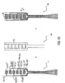
- the sensor array 10 includes a frame 15 and a plurality of sensor elements 20.
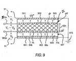
- the sensor array 10 is configured with a center core layer 75 and opposing (PVDF) outer layers 50, 60 which include piezoelectric layers 500 and 600.
- each of the (PVDF) outer layers 50, 60 provides a pair of spatially separated electrodes 501, 502, and 601, 602 which define first and second signal voltages 51, 61 with respect to ground 675.
- each of the outer layers 50, 60 have an external surface 50a, 60b which is electrically tied to the same electrical ground 675.
- the two opposing outer layer electrode surfaces 501, 502 and 601, 602 are configured to provide separate electrical signal paths ( i .
- the signal surfaces 50b, 60a are preferably provided by positioning signal traces 22 ( Figure 7) on the appropriate surface of the PVDF layer 50, 60. That is, as shown, the inner facing surfaces of the PVDF layers 50b, 60a , include electrical traces formed thereon.
- the outer ground plane or surfaces 675 are preferably provided by applying a conductive layer onto the outer faces of the PVDF layers 50a, 60b .
- a conductive layer onto the outer faces of the PVDF layers 50a, 60b .
- any metal depositing or layering technique can be employed such as electron beam evaporation, thermal evaporation, painting, spraying, dipping, or sputtering a conductive material or metallic paint and the like or material over the selected surfaces of the PVDF layers 50, 60.
- the ground plane is preferably formed by applying a continuous metallized surface over the entire outer surfaces of the PVDF layers 50a, 60b to form a continuous shield.
- conductive paint or ink (such as silver or gold) is applied to the PVDF layers as a thin planar layer such that it does not extend above or around the perimeter edge portions of the signal paths of the internal traces 22, 22' .
- the sensor array 10 includes a frame portion 15 with two longitudinally extending side rails, a first side rail 16, and a second side rail 17.
- the frame 15 is configured such that the two side rails 16, 17 are spatially separate along a major portion of the length of the frame 15.
- a plurality of sensor elements 20 are positioned intermediate the two side rails 16 and 17 such that each sensor element 20 is attached to at least one of the sides 16,17.
- each sensor element 20 is attached to only one side, i.e ., at a lateral attachment 18 positioned either at the first side 16 or the second side 17.
- adjacent sensors are attached to different sides of the frame 15 and the lateral attachments 18 extend substantially about the center of the sensor element 20.
- the sensor array 10 includes a first and second signal trace pattern 22, 22'.
- the trace patterns 22, 22' are the same and are configured to define two separate but corresponding active sensor electrical signal regions 25, 26, 27, 28, 29, 30 and 25', 26', 27', 28', 29', 30' across the upper and lower PVDF film layer sensor elements 20, 20'.
- the sensor array 10 is configured such that each corresponding sensor element electrical signal region 25, 25', 26, 26', 27, 27', 28, 28', 29, 29' and 30, 30' has a separate and corresponding electrical signal path 25a, 25a', 26a, 26a', 27a, 27a', 28a, 28a', 29a, 29a', 30a, 30a' respectively, defining corresponding but separate upper and lower signal paths 51, 61.
- each sensor 25a-30a extends from a sensor element 20 to an electrical termination or electrical connection pad 40.
- Figure 1A illustrates only one PVDF signal layer
- the opposing PVDF layer of the sensor array 10 includes another (second or bottom) signal trace pattern 22' substantially similar to and configured to align with the top external trace 22 pattern shown, including corresponding primed element numbers. That is, upon assembly or fabrication, two of the PVDF layers shown in the left side of Figure 1A are disposed on opposing sides of a neutral core 75.
- the electrical traces 22, 22' are applied to the respective PVDF outer layer 50, 60 such as by applying a silk screened conductive ink or paint pattern.
- the ground plane is preferably provided on each PVDF layer 50, 60 by applying a continuous layer of conductive ink or paint thereon.
- the core 75 typically includes a neoprene layer with a thin film of adhesive on each side.
- the PVDF layers 50, 60 are then secured to the core 75 to sandwich the core therebetween.
- the electrical connections (pin terminations) are made in an external connector and the upper and lower PVDF ground traces or surfaces 50a, 60b are connected to a common ground 675 thereat. See U.S. Patent No. 5,595,188.
- the sensor array 10' includes a frame 15' which can be configured to provide supplemental structural attachments 21 at selected areas (such as at the ends) to further structurally tie the two sides 16', 17' together to help provide structural strength or positional integrity for the sensor elements on the array 10'.
- This can be beneficial for sensor arrays 10' which, once sterilized, are enclosed in a sterile underlying adhesive layer and sterile package for shipment and storage, as the sensor array is typically quickly peeled from its packaging during use.
- the additional mechanical reinforcement can minimize sensor element 20 displacement from the frame 15'.
- Figure 5A illustrates another preferred embodiment of a sensor array 10" according to the present invention.
- the frame 15" includes a single longitudinally extending side or rail 17" which is preferably widened relative to the dual rail configuration shown in Figure 1B to provide adequate physical separation (to minimize the potential for electrical coupling) of the electrical traces 22b.
- the electrical traces 22b will be altered to extend along the single rail 17".
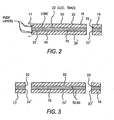
- FIGs 2 and 3 illustrate a section view of a preferred embodiment of the low profile sensor array 10.
- the sensor array 10 is configured such that the two piezoelectrically active (PVDF) outer layers 50, 60 of the sensor array 10 (including the outer layers of both the frame sides 16,17 and sensor elements 20) comprise a first material having an associated first thickness while a core or intermediate layer 75 comprises a second resilient material having a second thickness.
- PVDF piezoelectrically active
- Figure 9 schematically illustrates the electrical configuration of the sensor element 20 and will be discussed further below.
- the external traces 22 , 22' are positioned on the respective top and bottom surfaces 50b, 60a (i.e., the interior surfaces on a completed array assembly) of the outer layers 50, 60.
- the core 75 thickness is greater than the thickness of the outer layers 50, 60.
- the core 75 is an order of magnitude thicker than the outer layer thickness. More preferably, the core 75 has a depth or thickness of about 600 microns while the outer layers 50, 60 are about 30 microns thick. It is also preferred that the core material be selected such that it has a relative permittivity which is less (and more preferably much less such as an order of magnitude less) than the relative permittivity of the outer layers 50, 60. In one embodiment, a suitable core relative permittivity value is about 5 or 6.
- the core material 75 be selected such that it is resilient or compliant (substantially incompressible material) and preferably has low viscous losses.
- "Resilient" means that the core is sized and formed of a material which allows the sensor array (at least the sensor element) to be conformal to the underlying surface when in position. Stated differently, the core 75 is configured such that at least the sensor elements 20 are substantially compliance matched with the body, i.e., to follow the shape of the underlying patient skin surface when positioned thereon.
- Preferred core materials include nitrile, neoprene, latex, polyethylene, or high-density polyethylene forms. In a preferred embodiment, the core material is neoprene.
- the core 75 can be formed as a thin layer of insulator (a neutral center), allowing the two opposing electrically active layers 50, 60 to be electrically separated and directly responsive to the flexure of the underlying surface.
- the core 75 has a first relative permittivity and the outer layers 50, 60 are first and second pliable material layers which have a second relative permittivity.
- the first relative permittivity is less than the second relative permittivity.
- the resulting capacitance of the core 75 may be such that it is about an order of magnitude less than the PVDF layers 50, 60.
- the core 75 is sized to have a greater thickness than the PVDF layers 50, 60.
- the sensor 20 is configured such that the capacitance of the core 75 is less than that of the electrodes defined by the PVDF layers 50, 60.
- the outer layers 50, 60 are formed from a piezoelectrically active material such as, but not limited to, polyvinylidene fluoride (PVDF) or its copolymer with trifluoroethylene (PVDF-TrFe).
- PVDF polyvinylidene fluoride
- PVDF-TrFe polyvinylidene fluoride
- electrodes 501, 502, 601, 602 are formed on both sides of the major surfaces of piezoelectric film 500, 600.
- the PVDF material provide outer layers 50, 60 which function as electrodes which can act as an electromechanical transducer and, as such, can be used as an acoustic sensor 20.
- the senor 20 is configured such that when the piezoelectric material is subjected to strain or stress (flexure or curvature displacement) an electric potential or voltage proportional to the magnitude of the strain or compression is developed across the thickness of the piezoelectric material. See e.g., U.S. Patent No. 5,885, 222.
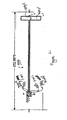
- Figure 4 is a side view of a low profile sensor array 10 according to a preferred embodiment of the present invention.
- the sensor array 10 is configured such that each of the sensor elements 25-30 and the frame 15 are in (substantially) coplanar alignment along at least the top surface 10a of a major portion of the frame 15 region when viewed from the side ( i . e ., the sensors 20 and sides 16, 17 have the same material thickness and layers). More preferably, as shown, the sensor array 10 (and the sensor array 10" with the single rail frame 15") is configured such that the elements 20 and the frame 15 have the same profile configuration along the top and bottom surfaces 10a, 10b. The sensor array 10 is substantially flush across the top and bottom surfaces 10a, 10b.
- the linear strip array preferably includes a top and bottom outer surface 10a, 10b with a substantially constant and flat profile.
- the top outer surface can include one or more discrete masses 900 or stiffeners 910 attached to the sensor element region to modify the response of the flexural sensor element 20 ( Figure 26).
- Figure 5 shows an alternate embodiment of a sensor array 10'.
- the lateral attachments 18' extend about alternating forward and rearward edges of the sensor elements 20.
- the sides or side rails 16',17' have a greater lateral length, providing additional area for the signal traces 22.
- the additional area can allow the separate paths to be spatially separated by a greater separation distance or can allow additional sensor elements 20 to be used (more area used for additional traces needed for the additional elements).
- the additional width of the sides 16', 17' can also help minimize electrical cross talk along the length of the signal path.
- Figure 5A illustrates a single-rail embodiment of a sensor array 10" according to the present invention.
- the sensor arrays 10,10', 10" include a plurality of sensor elements 20 (preferably more than four sensor elements, and more preferably six or more sensor elements).
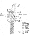
- the foundation layer 100 provides the structural foundation for the signal traces 22, 22' which are preferably applied to the PVDF layers 50, 60 and attached to the foundation layer 100, as will be discussed further below.
- the foundation layer 100 defines the frame 15, the side rails 16, 17 and the pads for the sensor elements 20. It also includes a neck portion 102 which separates the frame upper portion which includes a resilient core material to a thinner ribbon portion 105 (which extends down to the terminal connection ends at the connector (not shown)).
- the neck portion 102 of the frame 15 is preferably configured to transition the sensor array from one thickness to another such that the core 75 has a first thickness at the neck upper portion 102 but substantially terminates prior to the end of the neck lower portion 105 to a second reduced thickness.
- the sensor array 10 is configured such that the neoprene extends down until the area shown in cross hatch.
- a preferred neoprene stop zone 76 is shown at position A- A.
- the ribbon 105 is configured such that the PVDF electrically active surfaces do not contact.
- other thin insulating core materials such as a double sided polyethylene film can be positioned such that it extends between the two inwardly facing surfaces of the PVDF layers 50, 60.
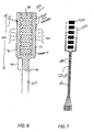
- Figure 7 illustrates a preferred trace pattern 22, 22' which is, upon assembly, positioned onto the appropriate surfaces of the film layers 50, 60 forming the respective electrical regions for the sensor elements 25-30, 25'-30' and respective signal paths 25a-30a, 25a'-30a' which extend down the neck portion 102 and ribbon portion 105 of the sensor frame.
- the electrical pattern 22, 22' includes a sensor pad active region 220 and linear traces 221.
- the trace pattern is disposed onto the piezoelectric layers 50, 60 as described above.
- it is formed by applying conductive ink, such as disposing onto the outer surfaces of the outer layers 50, 60 a silver ink silk screen pattern. While particular conductive patterns are illustrated in Figures 7 and 5A , alternative conductive patterns may also be used.
- conducting paint, flex circuits, foil or other coating or metal deposition methods and techniques may also be employed. It is preferred that, if flex circuits are used, that they are configured or attached to the foundation layer 100 so as to be transparent to the structure of the sensor array to minimize any potential interference with conformance of the sensor element to the body.
- protective films or coatings may also be positioned over the PVDF "outer” layers forming the ground and signal planes (or traces) as long as they are applied so as to be substantially transparent to the operation of the sensor elements. Therefore, as used herein, the trace(s) 22, 22' or outer layers 50, 60 can include traces or layers which are covered with moisture barrier coatings, adhesives, or other materials and are thus not truly "external” or “outer” as described for ease of discussion herein.
- Figure 8B is an enlarged view of a sensor element 20.
- the sensor element 20 is substantially rectangular with side dimensions of from about 8 mm to about 11 mm.
- the upper and lower traces 22, 22' are deposited onto the inwardly facing major surfaces of the (PVDF) layers 50, 60.
- the electrically active regions defining the signal paths include the pad regions 25, 25' and the signal lead paths 25a, 25a' which are spatially separated a distance from top to bottom about a central neutral core 75.
- the PVDF outer layers 50, 60 are preferably relatively thin (such as below about 60 microns, and preferably about 30 microns) while the core depth 75 a is an order of magnitude greater (above 300 microns, and more preferably above about 500 or 600 microns). This configuration makes the thickness of the PVDF layer 50, 60 relatively structurally negligible compared to the depth or thickness of the core 75. As shown in Figure 9 , the upper and lower signal paths 502a, 602a defined by the trace patterns 22, 22' are separated by a distance which is substantially equal to the core depth 75a.
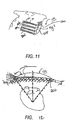
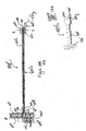
- Figure 10 schematically illustrates a preferred configuration of a low profile sensor array assembly 120.
- the sensor array assembly 120 includes four laterally positioned linear sensor or strip arrays 120a, 120b, 120c, 120d in electrical communication with a signal processor 150 (having an opto-isolator 151).
- Figure 10 illustrates four sensor arrays 10 positioned over preferred intercostal spaces. See WO-A-00/27287, U.S. Patents nos 6193668 and 6371924.
- Figure 10 also illustrates a preferred pigtail arrangement for the sensor array assembly 120.
- the pigtail 120P preferably extends off the sensor elements toward the sternum of the patient, thereby allowing standard cord sizing notwithstanding the access to the patient ( i . e ., whether the system must be hooked to the patient from the right or left hand side of the bed).
- the electrical pigtails 120P can extend from the opposing side.
- Figures 11 and 12 illustrate a preferred low profile sensor array 120 assembly positioned on a subject which comprises four linear array sensors 10, the sensors having six sensor elements 20 each.
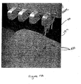
- Figure 12 illustrates the low profile acoustic sensor array 10 positioned on the skin 200 of a patient over an acoustic window above the cardiac region of interest.
- the sensor array according to the present invention preferably includes means for releasably securing the sensor array to a patient.
- Such means may comprise an adhesive layer which may be incorporated in or applied to one side of the sensor array such as the adhesive layer 775 shown in Figure 9 .
- the sensor array 10 also preferably includes a release adhesive 775 positioned along a major portion of the lower external surface 60b to secure the sensor array to a patient during clinical use.
- a release adhesive 775 positioned along a major portion of the lower external surface 60b to secure the sensor array to a patient during clinical use.
- sterile adhesive creams, double-sided tapes, and the like can alternatively or additionally be used to position the array on the patient's skin.
- Figure 9 illustrates the piezoelectric active outer layers 50, 60 as including a PVDF (or other piezoelectric polymer) portion 500, 600 and two corresponding opposing first and second interior active electrode surfaces or layers 501, 502 and 601, 602.
- the interior film surfaces 502, 602 each include a separate electrical signal path 502a, 602a while the outer film surfaces 501, 601 are tied to a common ground 675.
- Figures 9 and 13A-B illustrate that the PVDF is disposed on the first (upper) outer layer 50 with a polarity of negative to positive. That is, the major inner surface 50b has a positive polarity while the major outer surface 50a has a negative polarity.
- the PVDF is disposed on the (lower) outer layer 60 with the reverse polarity; positive on the major inner surface 60a, and negative on the major outer surface 60b.
- the layer polarities could also be reversed ( i . e ., the upper layer 50 can have negative to positive while the bottom layer 60 can have positive to negative).
- each of the outer layers 50, 60 provides a voltage (V 1 and V 2 ) 51, 61 in response to flexure of the sensor 20, respectively, even in response to long compressional waves.
- V 1 and V 2 voltage
- no voltage will result.
- the absolute value of the voltages for a particular flex or curvature will be substantially the same.
- the sign of the voltage will be opposite between the two layers.
- the instant sensor configuration is preferably configured to read the voltage differential of the two voltages, that is the difference between the response voltages V 1 , V 2 .
- the electrode configuration is such that the sensor 20 acts like a differential amplifier 63.
- the sensor array 10 takes the voltage differential of the two response voltages V,, V 2 to generate a signal response which has an increased voltage value (approximately doubled value) and, thus, can provide improved SNR performance.
- the voltage polarities are such that the signal responses from each layer 50, 60 cancel each other, minimizing signal output for non-flexure excitations.
- both the top and bottom sensor layers see the same force, and without a strain or flexure to cause a curvature in the layers 50, 60 the polarity of the voltages are such that any signal response is cancelled and no signal output is transmitted for detection.
- the polarities of the layers 50, 60 associated with the strain in the PVDF or outer (electrical response) layers 50, 60 have opposing polarities.
- the (V 2 ) response may be about (-2 microvolts), and the signal response for this flexure will then be 2-(-2) or 4 microvolts.
- the magnitude of the voltage will vary according to the degree of strain or curvature of the flexure.
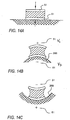
- Figure 14a illustrates the substantial non-response associated with a compression or longer wavelength transmitted across the sensor situs while Figures 14b and 14c show the voltage response (opposing polarity) corresponding to flexure at shorter wavelengths of interest.
- the voltage polarity corresponding to an upward flexure is positive for the upper PVDF layer 50 and negative for the lower PVDF layer 60 and the polarities reverse for a downward flexure.
- the sensor arrays 10, 10', 10", 10"' are configured such that they are selectively responsive to shorter wavelengths 310 that cause flexure through the thickness of the sensor element 20, 420, while being substantially non-responsive or resistant to longer acoustic wavelengths 300.
- the longer wavelengths 300 are typically associated with compression waves in the body or in the ambient noise within the examining room, and which cause compression through the thickness of the sensor element. In operation, due to differences in the speed of the waves or a frequency band of interest, shear waves typically have much shorter wavelengths than the wavelengths associated with compression waves.
- the senor is responsive to the flexural mode of displacement caused by short wavelengths of shear waves 310, and substantially non-responsive to acoustic inputs of the much longer compression wavelengths 300.
- the sensor array is configured to respond to shear waves having shorter wavelengths 310.
- the sensor array 10 of the present invention acts as a mechanical filter and inhibits or minimizes the sensor elements from generating a detectable signal response for long wavelengths at frequencies of interest.
- the sensors and sensor arrays described herein include an operational range for the acoustic wavelengths of interest for the diagnosis and detection of coronary artery disease.
- the sensors include an operational range of at least about 100-2500 Hz, and more preferably a range of about 100-1000 Hz.
- the sensor elements 20 are configured and sized on the frame 17 to respond to shear waves at the operating frequencies of interest such as those characterized as having propagation velocities of less than about 25 m/s, or more in the range of about 5-15 m/s, and to suppress or inhibit signal response for compressional waves or acoustic waves having a propagation velocity above about 100m/s. More preferably, the sensor is configured to suppress response associated with the wave speed of compressional waves in the air, typically a velocity of about 340 m/s and the response associated with the wave speed of compressional waves in the body, the compressional wave velocities being typically about 1540 m/s in the body.
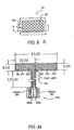
- Figure 8A illustrates an alternative discrete or single sensor embodiment of the present invention.
- the signal return covering the back of the film has been removed for clarity. It is preferred that the width of the pigtail be configured and sized to hold the capacitance of a signal trace below about 10% of that of a sensor element.
- the single sensor 201 includes a positive signal 280 and negative signal 281 electrical path which is formed by the two PVDF layers 50j, 60j similar to the electrical traces 322,322' formed onto the outer PVDF layers of the strip array 10 discussed above.
- the single element 201 can be formed by configuring four signal lines on a single sheet of PVDF material.
- the single sheet is configured to be folded, such as along the dotted fold lines shown, to provide the two interior signal paths 280, 281 and the external common ground.
- the two grounds 290a, 290b are preferably formed by a metallized mylar shield 290 configured to provide a continuous planar electrical shield on one surface of the PVDF material (the surface opposing the electrical traces 322, 322').
- the electrical pin out can also be alternatively configured as will be appreciated by one of skill in the art.
- Figures 17A and 17B illustrate yet another preferred embodiment of an accordion pleated sensor array 10"' which can advantageously minimize mechanical vibration and cross-talk between sensor elements 421, 422, 423 and their associated transmission lines 431, 432, 433 while also providing a mechanical filter (to reject compression energy and allow selective acoustic response as discussed above) according to the present invention.
- This low profile acoustic accordion array is also configured to selectively respond to shear waves while rejecting compression wave energy in the frequency range of interest.
- this sensor array 10"' includes multiple discrete or unitized sensors 420 and corresponding individual transmission lines 430 which are electrically connected at a primary connector 450 and into the signal processor operating system 150I.
- the sensor array 10"' preferably includes three sensor elements 421, 422, 423 with corresponding transmission lines 431, 432, 433.
- the separate transmission lines 431, 432, 433 can substantially isolate each element and respective transmission line to thereby minimize the cross talk between adjacent sensor elements.
- the transmission lines 431, 432, 433 are preferably folded or formed with a series of undulations 435 along the length of the transmission path (the transmission path extending between the sensor element 420 to the primary connector 450).
- the transmission line can be formed with a series of sinusoidal curves or waves or folds formed along a portion of its length, or formed with alternating material widths ( e . g ., thin to wide, wide to thin), or a combination of fold or curve patterns, interposed extra material or alternating material composition, weight, and the like.
- the term "undulating" includes the above mechanical damping configurations.
- Figures 17A and 17B illustrate a preferred sensor array 10'" alignment.
- the sensor array 10' positions the sensor pads 421, 422, 423 such that the discrete sensor pads are configured as an array 10'" with a plurality of unitized, separated, or discrete sensors; that is, the sensors 421, 422, 423 and corresponding transmission lines 431, 432, 433 are configured as discrete aligned segments in the array, i . e ., they have "unitized separation".
- the rear of the sensor pad 423b of the most distal sensor 423 is proximate to the front 422a of the next adjacent sensor pad 422.
- each of the sensor pads is conformal to the underlying skin and the transmission lines are sized and configured such each is spatially separated from the others ( i . e ., non-contacting with the others).
- the transmission line 430 preferably longitudinally extends off one end portion of the sensor pad (shown as the rear portion) 423b, 422b, 421b.
- the sensor array 10"' is configured and sized such that the transmission line for each sensor 430 extends off the sensor pad in a manner that, when connected to the system connector 450 and securely attached to the surface of the patient, the transmission line 430 defines a concave contour along a portion of its length when viewed from the side. That is, as shown by Figures 17A and 17B , the length of the transmission line 430 is such that it is sufficiently long when in position so as to provide a suitable amount of slack to prevent tensioning of the transmission line when the primary connector 450 is connected to the signal processing input port 150I.
- the sensor array 10"' is configured such that the array includes three discrete sensors 420, and each sensor 420, sensor pad 421-423, and associated transmission line 430 is a substantial mirror image of the other sensors, sensor pads, and transmission lines.
- the sensor array 10'" can include alternative numbers of sensors such as 2, 4, 5 or more.
- the system can employ several of the multi-element sensor arrays 10"' (such as four) of the tri-sensor discrete element sensor array 10"' (not shown). This plurality of three element sensor arrays 10"' can reduce the number of patient interconnections undertaken by a technician at patient application in order to prepare the equipment for use, while still allowing twelve individual sensor pad elements to be used for more precise acoustic detection on a patient.
- Figure 17A also illustrates a reflector 424 positioned on each of the sensor elements 420 to facilitate the detection system's photogrammetric recognition of the positional alignment of the sensor elements 420 when on the body.
- the reflector 424 can be applied by various means such as via reflective paint or by attaching reflective tape to the external (exposed) surface of the sensor element 420. See e . g ., co-pending and co-assigned U.S. Patent Application identified by Attorney Docket No. 9023-11IP, to Van Horn, entitled “Methods, Systems, and Computer Program Products for Photogrammetric Sensor Position Estimation.”
- the sensor body 420b includes a thin layer of piezoelectric film 420f ("PVDF") having opposing first and second major surfaces 420f a , 420f b .
- the first major surface 420f, of the film includes an active metallized electrode surface 22e defining the opposing sensor pad regions 420p1, 420p2.
- the first major surface 420f a also includes the separate electrical traces 480, 481.
- the electrical traces outside the electrode regions are inactive, for example, by the trace regions not being initially polarized, or depolarized such that they act to carry or transmit flexure signal generated by the electrode sensing regions.
- the second major surface 420f b of the PVDF film layer 420f (the surface underlying the exposed surface shown in Figure 18A) is formed from a conductive trace such as a conductive ink (but of course other methods for disposing a conductive trace can also be used such as those described hereinabove).
- the second major surface 420f b is preferably configured to provide a continuous conductive active surface pattern 22e' which includes the upper portion of the "T" defined by the two pad portions of the sensor body 420p1, 420p2.
- the second major surface 420f b also includes a trace 438g positioned along one side of the (PVDF film). This third transmission line or trace 438g acts as a ground signal path or line.
- the trace 438g is preferably configured to extend a greater distance on the termination end of the sensor 440 and thus form the long finger portion 440f of the termination end of the sensor. This additional length allows this portion of the sensor to be folded over to the other side of the sensor to align the ground signal line 438g with the signal transmission lines 438b, 438c for each of the electrodes 450, 460.
- this termination configuration provides a four point termination, one each associated with the electric shield "ground" 438a, the PVDF film layer traces 438b, 438c, and the folded 438g ground trace.
- the four-point termination connection for the primary connector 450 is thus configured on a single common connection surface.
- the PVDF film layer 420f defines the acoustic sensor signal paths 480, 481, and ground signal path 438g for each of the sensor pads or electrodes 450, 460, including the active portion of the sensor pad 420p1, 420p2 and the associated transmission or signal paths 438b, 438c, 438g. Similar to the operation of the differential sensor 63 explained for Figure 13 and 13A, the PVDF film 420f is preferably configured to provide opposing sensor pads 420p1, 420p2 which act as electrodes 450, 460 having opposing polarities. As shown in Figure 19B, the negative and positive polarity associated with the upper and lower electrodes 450, 460 provide the differential configuration for the flexure induced voltages v 1 , v 2 .
- the polarities can also be reversed, but the sensor region is preferably configured with opposing polarities for the sensor pad in order to provide the differential based operational sensing configuration.
- the PVDF film layer 420f is configured to provide an upper electrode surface and a lower electrode surface 450, 460, respectively (the lower electrode surface and the surface shown in Figure 18A disposed on the patient such that these surfaces face the skin of the patient).
- a layer of nonconductive material (such as polyester film) 499 is attached to or applied to overlie substantially the entire length of both sides of the PVDF film layer 420f along the linear transmission line 430 or trace portion of the sensor body 420b (excluding both sides of the sensor pads 420p1, 420p2 or upper portion of the "T" region of the sensor body).
- the polyester film layers 499 end a distance away from the termination end of the sensor 440 - substantially along a line shown by P-P in Figure 18A and Figure 20B.
- a single sided or double sided adhesive-backed polyester tape can be conveniently used to attach the polyester layers to the respective PVDF film surface 420f a , 420f b .
- other adhesive or attachment means can also be used as will be appreciated by one of skill in the art.
- the sensor body 420b also includes a resilient core 75' which is applied to one side of the sensor pad region of the sensor body 420b as shown by the arrow associated with the core element 75' drawn in dotted line in Figure 18A.
- Figure 19A also shows the preferred assembly position of the core 75' relative to the sensor pad 420p2 region of the sensor body 420b. In position, the core 75' is positioned to overlie and attach to the sensor pad 420p2 (such as via an adhesive).
- the PVDF film sensor pad 420p1 is folded over the central core layer 75' to overlie the opposing PVDF film sensor pad 420p2 as shown in cross section in Figure 19B.
- first and second layers of conductive shielding material layers 501, 502 are attached to the sensor body 420b.
- the shielding material layers are metallized film, and more preferably a thin sheet of MYLAR® film.
- the conductive shielding material layers 501, 502 help to shield the sensor 420 to minimize the introduction of electromagnetic interference into the sensor signal paths.
- the shielding material layers 501, 502 are sized and configured so that they do not contact along the sensor pad region of the sensor, i.e., the perimeter edges of the sensor pad are not enclosed by the shielding material layers 501, 502 when the PVDF film sensor pads are aligned over the core 75 '.
- the first shielding layer 501 linearly extends from the upper neck portion of the sensor body to an end portion which is adjacent the termination end of the sensor 440.
- the first shielding layer does not extend to cover the PVDF sensor pad regions 420p1, 420p2.
- the first shielding layer 501 ends at substantially the same position as the polyester layer 499 but also includes a termination protrusion end 438a which longitudinally extends a further distance to align with the active signal transmission lines 438b, 438c.
- Figure 20A shows the preferred end point for the non-conducting layers 499 and the upper shielding layer 501. As shown, the material extends adjacent but below the sensor pad regions 420p1, 420p2.
- Figure 20B shows the outer shielding material layer 501 positioned on the PVDF film layer 420f. As noted, the shielding layer 501 and the intermediately positioned polyester layer 499 end at a common termination line P-P for a major portion of the outer shielding material layer 501. This configuration allows electrical access for the signal lines 438b, 438c. This configuration also allows for electrical engagement with the ground path 438g when it is folded up to contact the shielding material layer 501.
- the second or opposing outer shielding layer 502 is configured and sized to substantially conform to the shape and size of the unfolded PVDF film layer 420f. As such, it includes a "T" shaped body of which the upper portion is preferably folded along with the sensor pad 420p1. When folded, the second shielding layer 502 provides a continuous electric shield for the exposed major surfaces of the sensor pad 420p and also preferably ends into or contacts the upper portion of the first shielding layer 501a at a lower edge 502a.
- the two opposing shielding layers 501, 502 provide a contiguous shield for the sensor 420 as shown in Figure 17A while the insulating polyester film layer maintains the electrical integrity of the internally disposed signal paths 438b, 438c.
- the second shielding layer 502 Similar to the first shielding layer 501, the second shielding layer 502 also includes a longitudinally extending protrusion portion 438a' positioned to overlie the first protrusion 438a with the PVDF film layer 420f disposed therebetween. Upon termination into the connector, the protrusion portions 438a, 438a' provide the electrical continuity for the shield layers 501; 502.
- Figure 21 illustrates the electrical signal paths 438a, 438b, 438c, and 438g formed onto the sensor body 420b.
- the live signal paths with opposing polarity are 438b and 438c, while the ground is provided by 438g and the shield by 438a, 438a'.
- the electrode configuration 450, 460 is such that the sensor 420 acts like a differential amplifier 63' as discussed for the embodiment described above.
- the sensor 420 takes the voltage differential of the two response voltages v 1 , v 2 to generate a signal response which has an increased voltage-value (approximately doubled value) and, thus, can provide improved SNR performance.
- the voltage polarities are such that the signal responses from each layer 450, 460 cancel each other, minimizing signal output for non-flexure excitations.
- the sensor component materials such as for the core are selected and configured as described for the first embodiment described herein.
- Another preferred embodiment of the present invention includes a sensor array 10"'M as shown in Figure 22A.
- at least one discrete mass 900 or external flex stiffener 910 is added to the upper (exposed when on a patient) surface of each sensor element 420.
- This configuration can modify the flexural response of the sensor element 420 and may improve the coupling of the sensor.
- the discrete mass 900 or external stiffener 910 extends across at least a portion of the short dimension of the sensor element. It is also preferred that the mass (or stiffener) be sized and configured on the sensor element 420 such that it is locally discrete as opposed to distributed (distributed meaning extending continuously across the long dimension of the sensor element).
- a centrally positioned discrete mass is positioned on each sensor element 420.
- the mass is formed from a high-density material such as a tungsten alloy, lead, or other heavy metal.
- a suitable discrete mass 900 weighs about 3-6 grams, and more preferably about 4.5-5 grams. Typical dimensions of the discrete mass is about 5 ⁇ 1 x 5 ⁇ 1 x 1 0 ⁇ 7 mm (0.2 x 02 x 0.42 inches) (or about a 5mm length across the short dimension of the sensor pad).
- Examples of discrete external stiffeners include a layer of material having a different (more rigid) stiffness as compared to the PVDF layers or the core.
- Figures 22A-E, 23A-C, and Figure 24 illustrate exemplary discrete mass and stiffener configurations according to the present invention.
- Figure 22B illustrates a plurality of discrete masses 901 positioned on opposing ends of the sensor elements 420.
- Figure 24 illustrates a discrete mass 900 positioned on the strip array 10.
- Figure 22C illustrates a discrete mass 900 positioned on the sensor element 420 and a discrete mass 900 and a second discrete mass 900a positioned on the transmission path 430.
- Figure 22D illustrates a plurality of discrete masses 900 positioned onto the sensor pad 420.
- Figure 22E shows a,plurality of alternately configured discrete elements 902 positioned on the sensor element 420.
- Figure 23A illustrates a pair of opposing external stiffeners 910 positioned onto the sensor element 420 while
- Figure 23C illustrates a single center stiffener 910.
- Figure 23B shows that the stiffener 910 can be combined with a discrete mass
- the reflectors ( 424, Figure 18A) or a reflective material can also be conveniently applied to the exposed surface of the stiffener 910 or discrete mass 900 to facilitate system positional operational alignment as discussed above.
- the stiffness of the sensor element 20, 420 can be adjusted by selecting the core materials to provide a different more stiff resilience at one or more regions in the pad such that the stiffer regions extend in at least one region across at least a portion of the short side of the sensor.
- the sensor array 10 is fabricated as a unitary body. That is, unlike conventional sensors, there is no requirement to assemble discrete sensor elements onto an underlying electrical ribbon.
- the frame 15 and sensor elements 20 are configured as a unitary body, and more preferably, the sensor array itself 10 is an entirely unitary body ( i . e ., a single piece construction comprising multiple layers but no discrete components excepting an electrical interface connector (not shown) which is adapted to be engaged with the electrical terminations 40 ).
- the core 75' be extruded, molded, formed, or cut, and that after the electric shield layer and other layers are positioned (and the sensor pad folded), the undulations be formed by mechanically crimping the assembled sensor at desired spacings along its length.
- the crimping means or forming means such as specialized tooling can also be used to configure the undulations onto the sensor body as will be appreciated by those of skill in the art.
- Figure 16 shows a block diagram describing a preferred method of fabricating a low profile sensor having two separate PVDF layers according to the first described embodiment.
- the foundation or core is formed (i.e., such as cut or extruded)
- the outer layers 50, 60 are attached thereon to form the strip sensor (Block 300).
- the foundation layer is cut so that a series of proximately located and non-contacting pads are formed onto a frame segment in the foundation layer (Block 310).
- An electrical signal path is positioned onto each of the outer layers (PVDF film) which is then secured to the foundation layer ( Block 330 ).
- the PVDF film may be selectively activated, i.e., only selected regions such as the sensor pad regions are actively polarized.
- selected portions of the PVDF film may be substantially deactivated by applying heat thereto (Block 350) .
- the material in order to appreciably enhance the piezoelectric effect in the PVDF material, the material is typically exposed to an appropriate electrical poling potential across the thickness of the film for an extended period of time.
- selectively activating" or “selectively polarizing” thus means exposing selected regions of the PVDF material to an electrical poling potential to enhance the piezoelectric effect in the film.
- exposing only the sensor pad regions and not the rails can minimize the "active" nature of the rails and/or non-sensing areas of the PVDF film thereby providing substantially “non-active” regions.
- the entire sensor can be subjected to the electrical poling potential, and then the rails can be "de-poled” such as by heating. Alternately, of course, "selective polarization or activation” is not required.
- the entire PVDF film employed in the sensor can remain piezoelectrically enhanced or "activated”.
- Figure 16A illustrates additional preferred method steps.
- the frame segment is formed such that it includes a pair of longitudinal sides and the series of non-contacting pads are arranged to attach to one side of the frame segment (Block 312).
- a pattern defining a plurality of electrically separate external traces are disposed onto a surface of each of two PVDF layers (defining a corresponding top and bottom electrical trace which is associated with each of the longitudinally extending opposing sides and the sensor pads) (Block 335).
- the disposing step is performed by applying a conductive layer with a trace pattern such as via conductive ink and the two PVDF layers are attached to the foundation layer such that the signal traces face each other and contact the foundation layer. (Block 345).
- a neoprene core material is inserted into a die.
- the PVDF material is preferably introduced onto the core layer 75 (75') such that a first outer layer 50 has a first polarity and a second outer layer 60 positioned contacting the core 75 opposing the first outer layer 50 has a second polarity, the second polarity being the reverse of the first polarity.
- the fabrication process introduces the core material into the forming, cutting or extruding machine such that it terminates in the finished extruded product at a longitudinal distance away from the frame along the foundation layer (100, Figure 6).
- the frame pattern is then cut to form the foundation layer (which includes the core 75 and two opposing outer layers 50, 60 as discussed above).
- the foundation layer defines a linear arrangement of a plurality of sensor pads.
- An electrical signal path is positioned onto the external surface of the foundation layer 100.
- the electrical trace pattern is introduced onto the PVDF layer by applying a conductive ink in a silk screen pattern thereon.
- a conductive electrical trace pattern is disposed onto two (preferably planar) separate surfaces of the two PVDF layers , the top outer surface and the bottom outer surface 50, 60.
- the electrical pattern includes a sensor pad active region 220 and linear traces 221.
- the same pattern is disposed as an external trace onto each transverse outer surface, such that the sensor array has two separate signal paths for each element 20, the signal paths separated by the core material depth or thickness.
- the PVDF can be selectively polarized or selected portions of the outer layers can be de-polarized.
- the frame portions which carry the linear external trace portions can be non-activated or heated to deactivate the PVDF material in that area to minimize the potential for signal excitation in this area so as to inhibit interaction or activation along the length of the array.
- Figure 19A shows a preferred method of fabricating a low profile sensor having discrete elements as shown in Figure 17A.
- a first unitary layer of PVDF film is configured with a laterally extending portion having a first width and a longitudinally extending portion having a second width.
- the longitudinally extending portion preferably extends from a lower edge of a center of the lateral portion, thus forming a "T" shape configuration.
- Electrical traces are formed onto both major surfaces of the PVDF layer.
- the electrical traces are formed as a rectangular shaped sensor element onto the upper or lateral portion of the "T” such that this portion defines the two separate electrode regions with opposing polarity.
- the electrical traces are formed onto the lower portion of the "T" to define three electrical paths.
- the first and second paths are formed on one major surface adjacent to one side to provide the electrical signal path for the first and second electrodes.
- the third path is formed on the opposite side of the PVDF layer (on the second major surface).
- the third path preferably includes a primary finger portion.
- the third path forms the electrical ground and extends along the side of the second major surface opposite the side the first and second paths are formed on the first major surface.
- a resilient core (such as neoprene) is inserted onto the top surface of one of the electrode regions.
- Linear strips of non-conducting film is positioned to overlay the lower portion of the "T".
- a first electric shield material (such as MYLAR®) is positioned to overlay the lower portion of the "T” over the non-conducting (polyester) film on the side opposing the first major surface of the PVDF film (the side with the first and second electrical paths) and preferably includes a conductive finger portion.
- This conductive shield layer does not extend into the electrode region.
- a "T" shaped conductive shield layer is configured and sized to mirror the PVDF film shape. This outer conductive shield layer is positioned to overlay the second major surface of the PVDF film in the electrode region and to overlay and contact the non-conducting film in the linear transmission layer.
- the laterally extending portion of the PVDF film with the outer shield thereon is folded over the neoprene core such that the first and second electrode regions are positioned opposing the other with the core in contact with each and positioned intermediate thereof.
- the finger of the ground strip is folded up to contact the first conductive shield material thereby providing a substantially continuous electric shield for the sensor while maintaining the electrical integrity of the electrode sensors.
- the transmission line is then preferably crimped at predetermined portions to create the undulations along its length.
- the sensor is then preferably combined with a plurality of other sensors and packaged as a sensor array.
- the sensor array preferably includes a carrier member which is configured to hold the sensor elements in positional alignment until the sensor elements are secured to the patient.
- the carrier member can readily be detached from the individual sensor elements leaving them in place (in predetermined alignment) and structurally separate and physically isolated from the others.
- the sensor array is configured with a plurality of unitized sensors held by a unitizing member, and after applying the unitized array to a patient, the unitized member is readily removed leaving the sensors secured to a patient in a predetermined alignment.
- the instant invention can provide a low profile sensor package which can be more responsive to acoustic signals measured on the external epidermal layer (conforms to patient chest area and flexes in response to chest movement). Further, the instant invention provides a smaller array package with closely positioned separately electrically activated sensor elements thereby allowing additional sensors in a smaller region to allow a more discerning sensor measurement. Further, the sensor array can selectively respond to the shorter wavelengths for the acoustic wave input of interest particularly those associated with evaluating coronary artery disease.
- the PVDF can be selectively activated in the sensor pad region as described above (or the PVDF be deactivated in the non-sensor pad region, preferably at least along the electrical traces) for all of the embodiments described herein.
- the sensor elements 20, 420 can be alternatively configured such as but not limited to a triangle, square, circle, parallelogram, octagon, and the like.
- the discrete masses 900 or external stiffeners 910 can also be configured in alternative shapes such as but not limited to a triangle, square, circle, parallelogram, octagon, and the like.
- the present invention may also take the form of a single frame or single rail member with sensors formed on one or both sides of the frame or rail or alternatively, discrete element sensors. Accordingly, the present invention should not be construed as limited to structures with a particular number of frame members or with a particular configuration of the frame but should encompass any frame structure or discrete sensor structure which allows for the differential operation of the sensor array according to the present invention.
Abstract
Description
Claims (32)
- A low profile acoustic sensor array (10, 10', 10", 10'"), comprising:characterised in that said plurality of sensor element pads (20, 420) comprises a plurality of discrete aligned along said primary direction spaced apart conformable acoustic sensor element pads (20, 420), and said at least one longitudinally extending elongate strip (16, 16', 17, 17', 17", 430) is integrally attached to at least one of said plurality of acoustic sensor pads, wherein a respective elongate strip is configured so that the at least one integrally attached acoustic sensor element pad extends outwardly away from the primary direction of the strip, the number of discrete electrical transmission paths (22, 22', 280, 281, 322, 322', 438b, 438c, 480, 481) on the strip corresponding to the number of acoustic sensor element pads held by the strip with a respective acoustic sensor element configured to be in electrical communication with a respective electrical transmission path.a plurality of sensor element pads (20, 420), each including an active sensing element comprising piezoelectric material, wherein each sensor element pad (20, 420) is conformable to a shape of an underlying structure, and wherein, in operation, the sensor element pads are configured to generate an electrical signal in response to flexure induced by acoustic signals; andat least one longitudinally extending elongate strip (16, 16', 17, 17', 17", 430) defining a primary direction, the elongate strip having length with opposing first and second end portions, the elongate strip comprising at least one discrete electrical transmission path (22, 22', 280, 281, 322, 322', 438b, 438c, 480, 481) thereon, the second end portion of the elongate strip adapted to connect to an output device,
- A low profile acoustic sensor array according to Claim 1, wherein the at least one acoustic sensor element pad (20, 420) is substantially planar when viewed from the side and configured to releaseably attach to skin of a subject, and wherein, in operation, opposing primary surfaces (50, 60, 450, 460) of the acoustic sensor element pad concurrently flex in response to detected acoustic waves transmitted from the subject.
- A low profile acoustic sensor array according to Claim 1 or 2, wherein the at least one strip (16, 16', 17, 17', 17") is substantially planar along a major portion thereof when viewed from the side.
- A low profile acoustic sensor array according to any one of Claims 1 to 3, wherein the plurality of acoustic sensor element pads (20) are configured as a plurality of longitudinally spaced apart acoustic sensor element pads attached to a common strip (16, 16', 17, 17', 17").
- A low profile acoustic sensor according to any one of Claims 1 to 4, wherein each of the at least one acoustic sensor element pad (20, 420) extends substantially perpendicularly away from the primary direction of the strip (16, 16', 17, 17', 17", 430).
- A low profile acoustic sensor array according to any one of Claims 1 to 3 and 5, wherein the at least one strip comprises a plurality of strips (430), each having a respective one acoustic sensor element pad (420) positioned on an end portion thereof.
- A low profile acoustic sensor array according to any preceding Claim, wherein the at least one acoustic sensor element pad (20, 420) is configured as a substantially rectangular patch with adhesive on a primary surface thereof.
- A low profile acoustic sensor array according to any one of Claims 1 to 5 and 7, wherein each of the at least one strip (16, 16', 17, 17', 17") comprises a plurality of proximately positioned longitudinally aligned acoustic sensor element pads (20) with gap spaces therebetween.
- A low profile acoustic sensor array according to Claim 8, wherein the at least one strip comprises a neck portion (102) with a first width that terminates into a conformable sensor support frame (15, 15', 15"), the sensor support frame comprising at least one outer longitudinally extending conformable rail (16, 16', 17, 17', 17") extending about an outer perimeter edge portion thereof, and wherein the acoustic sensor element pads (20) are attached to and extend laterally away (18, 18') from the at least one longitudinally extending rail (16, 16' 17, 17' 17"), and wherein a respective electrical transmission path (22, 22', 280, 281, 480, 481) on the strip laterally extends (22b) from a corresponding acoustic sensor element pad (20) then turns to extend longitudinally about the at least one longitudinally extending rail (16, 16', 17, 17', 17"), with adjacent transmission paths on the longitudinally extending rail corresponding to adjacently positioned acoustic sensor pads.
- A low profile acoustic sensor array according to Claim 9, wherein the sensor support frame (15, 15') comprises two spaced apart longitudinally extending rails (16, 17; 16, 17') positioned at opposing perimeter edge portions thereof with the plurality of acoustic sensor elements (20) held therebetween.
- A low profile acoustic sensor array according to Claim 10, wherein each of said plurality of acoustic sensor elements (20) is attached to a respective one of said opposing frame rails (16, 17; 16, 17').
- A low profile acoustic sensor array according to Claim 10, further comprising gap spaces between adjacent sensor elements (25, 26, 27, 28, 29, 30), each sensor element configured to independently detect acoustic and vibratory energy to thereby respond to targeted acoustic wavelengths and to inhibit response to compressional wavelengths so as to mechanically filter acoustic signals detected by the sensor array.
- An acoustic sensor array according to any preceding Claim, wherein the strip (16, 16', 17, 17', 17", 430) is a unitary body along a major portion of its length.
- An acoustic sensor array according to any one of Claims 9 to 13, wherein said at least one longitudinally extending frame rail (16, 16', 17, 17', 17", 430) and said acoustic sensor element pads (20, 420) have an upper surface, and wherein said upper surface of said at least one frame rail and said sensor element pads have a substantially common constant flat contour when viewed from the side.
- An acoustic sensor array according to any one of Claims 1 to 14, further comprising a plurality of discrete masses (900, 901), at least one positioned to reside on a minor portion of an upper surface of each of said acoustic sensor element pads (20, 420).
- An acoustic sensor array according to any preceding Claim, wherein each of said sensor element pads (20, 420) comprises a first PVDF layer (50, 450) overlying and contacting a second flexible core layer (75, 75') and a third PVDF layer (60, 460) opposing said first layer and contacting said core layer.
- An acoustic sensor array according to Claim 16, wherein the strip transmission path (22, 22', 438b, 438c, 480, 481) for each respective sensor element (20, 420) thereon comprise a conductive pattern (22, 22', 25-30, 25'-30', 25a-30a, 25a'-30a', 322, 322', 438b, 438c, 438g, 480, 481) applied to said first and second PVDF film layers (50, 450; 60, 460).
- An acoustic array according to any one of Claims 9 to 17, wherein each of said at least one frame rail (16, 16', 17, 17', 17", 430) comprises a first PVDF layer (50, 450), a second intermediate core layer (75, 75'), and a third PVDF layer (60, 460), wherein said first and third PVDF layers sandwich said second core layer.
- An acoustic array according to Claim 18, wherein each of said at least one frame rail (16, 16', 17, 17', 17", 430) and said acoustic sensor pads (20, 420) comprise the same multi-layer materials in substantially the same thicknesses.
- An acoustic array according to Claim 19, wherein said first layer PVDF (50, 450) is selectively actively polarized about portions of the sensor elements on each acoustic sensor pad (20, 420) and substantially non-actively polarized about frame rail sides (16, 16', 17, 17', 17", 430) to thereby provide increased signal isolation.
- An acoustic sensor array according to any one of Claims 6 to 7 and 12 to 13, wherein said plurality of strips (16, 16', 17, 17', 17", 430) is at least three.
- An acoustic sensor array according to any one of Claims 8 to 20, wherein said at least one strip (16, 16', 17, 17', 17", 430) is at least four.
- An acoustic array according to any one of Claims 8 to 22, wherein said plurality of acoustic sensor elements (20) is six.
- An acoustic array according to Claim 18, wherein said strip electrical transmission path is defined by two spatially separate opposing electrical traces (22, 22', 25-30, 25'-30', 25a-30a, 25a'-30a', 322, 322', 438b, 438c, 438g, 480, 481) formed onto said first and third PVDF layers (50, 60; 450, 460), said separate electrical traces including a first electrical linear trace with a first substantially rectangular sensor element trace region (20, 22e, 420) and a corresponding second linear trace with a second substantially rectangular sensor element trace region (20, 420), wherein said first electrical linear trace and first rectangular trace region disposed onto said first PVDF layer (50, 450) and said second electrical linear trace and second rectangular trace region disposed onto said third PVDF layers (60, 460).
- An acoustic sensor array according to any one of Claims 1 to 15, wherein each acoustic sensor element comprises:a resilient core layer (75, 75') comprising a low permittivity material having a core thickness;a first conformable material layer (50, 450) overlaying and contacting said core layer, said first material layer comprising a piezoelectrically active material, said first conformable layer having opposing internal and external surfaces;a second conformable material layer (60, 460) overlaying and contacting said core layer opposing said first pliable material layer, said second conformable layer comprising a piezoelectrically active material and having opposing internal and external surfaces;a first electrical trace (22, 280, 322, 438b, 480) disposed on said first conformable material layer inner surface; anda second electrical trace (22', 281, 322', 438c, 481) disposed on said second conformable material layer inner surface such that said first and second electrical traces face each other across said core layer, wherein during operation and in response to flexure of said sensor element (20, 22e, 420), said first and second electrical traces concurrently generate respective first and second voltages of opposing polarity.
- An acoustic sensor according to any preceding Claim, wherein each of said acoustic sensor element pads (20, 420) are configured to concurrently generate first and second voltages of opposing polarity during flexure, and wherein the sensor array is configured to combine the first and second voltages to determine a voltage differential between the first and second voltages.
- A method for fabricating a strip sensor array according to claims 1 to 26 having a plurality of sensor elements thereon, comprising the steps of:forming a unitary body strip sensor foundation layer (100; 75) having opposing major surfaces;forming a series of proximately positioned non-contacting sensor element pads (20) and a frame segment (15, 15', 15") into the foundation layer (100);positioning two separate opposing PVDF layers (50, 60, 450, 460) on opposing major surfaces of the foundation layer (100), the PVDF layers including two major surfaces and an electrical signal path (22, 22') formed on one surface anda ground path formed on the other; andorienting the PVDF layers such that the electrical signal paths (220) of eachof the PVDF layers faces the foundation layer (75, 75').
- A method according to Claim 27, wherein said second forming step further comprises forming the frame segment (15, 15') to include two longitudinally extending spaced apart opposing side rails (16, 16', 17, 17'), and arranging the series of sensor element pads (20) on the foundation layer (100, 75) to attach to at least one of the two opposing side rails of the frame segment and to reside between the two opposing side rails.
- A method according to Claim 28, wherein said positioning step is performed by disposing a series of electrically separate conductive external traces (22) onto a first major surface of the PVDF layers, the conductive electrical traces including a linear extending signal path (221) and an electrode region (220) sized and configured to substantially correspond to the sensor element pads (20).
- A method according to Claim 29, further comprising disposing a series of discrete masses (900, 901) onto an exposed surface of one of the PVDF layers (50, 60, 450, 460) proximate the sensor element pads (20).
- A method according to Claim 30, wherein the PVDF layers (50, 60, 450, 460) of the sensor element pads (20) are configured to generate output voltages of opposing polarities in response to a flexure input.
- A method of detecting acoustic wave signals to identify the condition of a patient's coronary arteries, using the sensor arrays of any one of Claims 1 to 25, comprising:positioning the sensor array (10, 10', 10", 10"') onto a patient's exposed surface in a chest region of interest;securing each of said plurality of sensor elements (20, 420) to the patient such that they are conformal to the surface of a patient;flexurally displacing at least one sensor element (20, 420) in response to a detected shear wave in an acoustic frequency of interest, the flexural displacement generating a first voltage having a first polarity associated with said first piezoelectric active layer (50, 450) and a second voltage having an opposing polarity associated with said second piezoelectric active layer (60, 460); andcombining the first and second voltages to generate an output signal for the flexed sensor responsive to the change in curvature of the patient surface associated with the detected shear wave.
Priority Applications (1)
| Application Number | Priority Date | Filing Date | Title |
|---|---|---|---|
| EP04015375A EP1477237A3 (en) | 1999-03-01 | 2000-02-29 | Low profile acoustic sensor array and sensors with pleated transmission lines and related methods |
Applications Claiming Priority (5)
| Application Number | Priority Date | Filing Date | Title |
|---|---|---|---|
| US12226499P | 1999-03-01 | 1999-03-01 | |
| US122264P | 1999-03-01 | ||
| US13204199P | 1999-04-30 | 1999-04-30 | |
| US132041P | 1999-04-30 | ||
| PCT/US2000/005124 WO2000054897A2 (en) | 1999-03-01 | 2000-02-29 | Low profile acoustic sensor array and sensors with pleated transmission lines and related methods |
Related Child Applications (1)
| Application Number | Title | Priority Date | Filing Date |
|---|---|---|---|
| EP04015375A Division EP1477237A3 (en) | 1999-03-01 | 2000-02-29 | Low profile acoustic sensor array and sensors with pleated transmission lines and related methods |
Publications (2)
| Publication Number | Publication Date |
|---|---|
| EP1156891A2 EP1156891A2 (en) | 2001-11-28 |
| EP1156891B1 true EP1156891B1 (en) | 2005-11-30 |
Family
ID=26820347
Family Applications (2)
| Application Number | Title | Priority Date | Filing Date |
|---|---|---|---|
| EP00912045A Expired - Lifetime EP1156891B1 (en) | 1999-03-01 | 2000-02-29 | Low profile acoustic sensor array and sensors with pleated transmission lines and related methods |
| EP04015375A Withdrawn EP1477237A3 (en) | 1999-03-01 | 2000-02-29 | Low profile acoustic sensor array and sensors with pleated transmission lines and related methods |
Family Applications After (1)
| Application Number | Title | Priority Date | Filing Date |
|---|---|---|---|
| EP04015375A Withdrawn EP1477237A3 (en) | 1999-03-01 | 2000-02-29 | Low profile acoustic sensor array and sensors with pleated transmission lines and related methods |
Country Status (9)
| Country | Link |
|---|---|
| US (1) | US20050251047A1 (en) |
| EP (2) | EP1156891B1 (en) |
| JP (2) | JP3841197B2 (en) |
| AT (1) | ATE311260T1 (en) |
| AU (2) | AU2004201785B2 (en) |
| BR (1) | BR0008668A (en) |
| CA (1) | CA2361833C (en) |
| DE (1) | DE60024416T2 (en) |
| WO (1) | WO2000054897A2 (en) |
Cited By (1)
| Publication number | Priority date | Publication date | Assignee | Title |
|---|---|---|---|---|
| US11064292B2 (en) * | 2016-03-23 | 2021-07-13 | The Yokohama Rubber Co., Ltd. | Acoustic transmission member and method of designing same |
Families Citing this family (14)
| Publication number | Priority date | Publication date | Assignee | Title |
|---|---|---|---|---|
| JP4496476B2 (en) * | 2005-02-23 | 2010-07-07 | 株式会社デンソー | Vehicle collision detection sensor and vehicle collision object discrimination device using the same |
| US7520860B2 (en) | 2005-04-13 | 2009-04-21 | Marie G. Johnson | Detection of coronary artery disease using an electronic stethoscope |
| US20080139893A1 (en) * | 2006-12-08 | 2008-06-12 | Warren Lee | Apparatus And System For Sensing and Analyzing Body Sounds |
| US20100204617A1 (en) * | 2009-02-12 | 2010-08-12 | Shmuel Ben-Ezra | Ultrasonic probe with acoustic output sensing |
| EP2585227B1 (en) | 2010-06-24 | 2022-02-09 | CVR Global, Inc. | Sensor, sensor pad and sensor array for detecting infrasonic acoustic signals |
| US11413653B2 (en) | 2010-06-24 | 2022-08-16 | Cvr Global, Inc. | Sensor, sensor pad and sensor array for detecting infrasonic acoustic signals |
| WO2013023041A2 (en) * | 2011-08-10 | 2013-02-14 | Aum Cardiovascular, Inc. | Devices, systems and methods for the detection of coronary artery disease |
| CN103946680A (en) * | 2011-09-28 | 2014-07-23 | Mc10股份有限公司 | Electronics for detection of a property of a surface |
| CN104185449B (en) | 2012-03-07 | 2016-08-24 | 瑞典计算机医疗技术有限公司 | Sensor and stethoscope |
| JP5928151B2 (en) * | 2012-05-21 | 2016-06-01 | セイコーエプソン株式会社 | Ultrasonic transducer, ultrasonic probe, diagnostic device and electronic equipment |
| US10828008B2 (en) | 2017-03-13 | 2020-11-10 | Biosense Webster (Israel) Ltd. | Steam pop detection |
| US10694999B2 (en) * | 2017-10-13 | 2020-06-30 | Case Western Reserve University | Conductive layer formed strain gauge and method of making same |
| EP3803468B1 (en) * | 2018-06-08 | 2023-11-08 | PGS Geophysical AS | Towed marine streamer having a linear array of piezoelectric transducers |
| US11638353B2 (en) * | 2018-09-17 | 2023-04-25 | Hutchinson Technology Incorporated | Apparatus and method for forming sensors with integrated electrical circuits on a substrate |
Family Cites Families (49)
| Publication number | Priority date | Publication date | Assignee | Title |
|---|---|---|---|---|
| BE785945A (en) * | 1971-07-06 | 1973-01-08 | Siemens Ag | ELECTRIC FILTER USING THE PRINCIPLE OF SURFACE WAVES |
| US3774592A (en) * | 1971-12-16 | 1973-11-27 | Xerox Corp | Method for providing an improved body electrode electrical connection |
| US4082086A (en) * | 1976-12-13 | 1978-04-04 | M I Systems, Inc. | Ecg monitoring pad |
| JPS5840805B2 (en) * | 1978-04-10 | 1983-09-08 | 東レ株式会社 | Coordinate input structure |
| US4376302A (en) * | 1978-04-13 | 1983-03-08 | The United States Of America As Represented By The Secretary Of The Navy | Piezoelectric polymer hydrophone |
| DE3069001D1 (en) * | 1979-05-16 | 1984-09-27 | Toray Industries | Piezoelectric vibration transducer |
| US4491051A (en) * | 1980-02-22 | 1985-01-01 | Barcus Lester M | String instrument pickup system |
| US4308870A (en) * | 1980-06-04 | 1982-01-05 | The Kendall Company | Vital signs monitor |
| IL67815A (en) * | 1982-02-12 | 1988-01-31 | Sanz Ernst | Method and apparatus for cardiogonometry |
| GB2117992B (en) * | 1982-03-24 | 1985-09-18 | Philips Electronic Associated | Parallel-series acoustic wave device arrangement |
| CA1198806A (en) * | 1982-11-24 | 1985-12-31 | Her Majesty The Queen, In Right Of Canada, As Represented By The Minister Of National Defence | Heart rate detector |
| US4586514A (en) * | 1983-08-10 | 1986-05-06 | Biotronics Instruments | Phonoangiographic spectral analysing apparatus |
| US4833659A (en) * | 1984-12-27 | 1989-05-23 | Westinghouse Electric Corp. | Sonar apparatus |
| US4862361A (en) * | 1985-06-05 | 1989-08-29 | Massachusetts Institute Of Technology | Methods and apparatus for monitoring cardiovascular regulation using heart rate power spectral analysis |
| US4777961A (en) * | 1985-10-15 | 1988-10-18 | Bruce Saltzman | High sensitivity stethoscopic system and method |
| US4792145A (en) * | 1985-11-05 | 1988-12-20 | Sound Enhancement Systems, Inc. | Electronic stethoscope system and method |
| JPH033289Y2 (en) * | 1987-01-26 | 1991-01-29 | ||
| DE3744605C1 (en) * | 1987-12-31 | 1989-04-27 | Jochen Dipl-Ing Heimann | Sensor |
| US4905706A (en) * | 1988-04-20 | 1990-03-06 | Nippon Colin Co., Ltd. | Method an apparatus for detection of heart disease |
| US5164627A (en) * | 1988-07-26 | 1992-11-17 | Harris Corporation | Phased array acoustic signal processor |
| US4947859A (en) * | 1989-01-25 | 1990-08-14 | Cherne Medical, Inc. | Bio-acoustic signal sensing device |
| US5042481A (en) * | 1989-01-31 | 1991-08-27 | Sharp Kabushiki Kaisha | Body electrode holder |
| US5166573A (en) * | 1989-09-26 | 1992-11-24 | Atochem North America, Inc. | Ultrasonic contact transducer and array |
| US5036857A (en) * | 1989-10-26 | 1991-08-06 | Rutgers, The State University Of New Jersey | Noninvasive diagnostic system for coronary artery disease |
| US5109863A (en) * | 1989-10-26 | 1992-05-05 | Rutgers, The State University Of New Jersey | Noninvasive diagnostic system for coronary artery disease |
| US5301679A (en) * | 1991-05-31 | 1994-04-12 | Taylor Microtechnology, Inc. | Method and system for analysis of body sounds |
| US5337752A (en) * | 1992-05-21 | 1994-08-16 | Mcg International, Inc. | System for simultaneously producing and synchronizing spectral patterns of heart sounds and an ECG signal |
| US5365937A (en) * | 1992-09-09 | 1994-11-22 | Mcg International, Inc. | Disposable sensing device with contaneous conformance |
| AU6953994A (en) * | 1993-06-04 | 1995-01-03 | Regents Of The University Of California, The | Microfabricated acoustic source and receiver |
| US5398689A (en) * | 1993-06-16 | 1995-03-21 | Hewlett-Packard Company | Ultrasonic probe assembly and cable therefor |
| DE69415023T2 (en) * | 1993-08-30 | 1999-04-22 | Medacoustics Inc | DISPOSABLE CUSHION SENSOR |
| US5687738A (en) * | 1995-07-03 | 1997-11-18 | The Regents Of The University Of Colorado | Apparatus and methods for analyzing heart sounds |
| US5595188A (en) * | 1995-07-26 | 1997-01-21 | Flowscan, Inc. | Assembly process for polymer-based acoustic differential-output sensor |
| JP3789136B2 (en) * | 1995-07-28 | 2006-06-21 | ユニリード インターナショナル インコーポレイテッド | Disposable dermatoelectric device |
| US5638823A (en) * | 1995-08-28 | 1997-06-17 | Rutgers University | System and method for noninvasive detection of arterial stenosis |
| US5831492A (en) * | 1995-09-15 | 1998-11-03 | Sawtek Inc. | Weighted tapered spudt saw device |
| US5598845A (en) * | 1995-11-16 | 1997-02-04 | Stellartech Research Corporation | Ultrasound transducer device for continuous imaging of the heart and other body parts |
| US5727561A (en) * | 1996-04-23 | 1998-03-17 | The United States Of America As Represented By The Department Of The Navy | Method and apparatus for non-invasive detection and analysis of turbulent flow in a patient's blood vessels |
| US5853005A (en) * | 1996-05-02 | 1998-12-29 | The United States Of America As Represented By The Secretary Of The Army | Acoustic monitoring system |
| US5680863A (en) * | 1996-05-30 | 1997-10-28 | Acuson Corporation | Flexible ultrasonic transducers and related systems |
| US5827198A (en) * | 1996-11-21 | 1998-10-27 | Flowscan, Inc. | Low-cost, disposable, polymer-based, differential output flexure sensor and method of fabricating same |
| US5782767A (en) * | 1996-12-31 | 1998-07-21 | Diagnostic Ultrasound Corporation | Coupling pad for use with medical ultrasound devices |
| US5795299A (en) * | 1997-01-31 | 1998-08-18 | Acuson Corporation | Ultrasonic transducer assembly with extended flexible circuits |
| US5807271A (en) * | 1997-04-14 | 1998-09-15 | Tayebi; Sean | Fetal heartbeat and uterine contraction |
| US6193668B1 (en) * | 1997-11-10 | 2001-02-27 | Medacoustics, Inc. | Acoustic sensor array for non-invasive detection of coronary artery disease |
| US6278890B1 (en) * | 1998-11-09 | 2001-08-21 | Medacoustics, Inc. | Non-invasive turbulent blood flow imaging system |
| US6261237B1 (en) * | 1998-08-20 | 2001-07-17 | Medacoustics, Inc. | Thin film piezoelectric polymer sensor |
| US6178344B1 (en) * | 1999-03-02 | 2001-01-23 | The United States Of America As Represented By The Secretary Of The Navy | Reconfigurable array for positioning medical sensors |
| US6558323B2 (en) * | 2000-11-29 | 2003-05-06 | Olympus Optical Co., Ltd. | Ultrasound transducer array |
-
2000
- 2000-02-29 CA CA002361833A patent/CA2361833C/en not_active Expired - Fee Related
- 2000-02-29 AU AU2004201785A patent/AU2004201785B2/en not_active Ceased
- 2000-02-29 JP JP2000604961A patent/JP3841197B2/en not_active Expired - Fee Related
- 2000-02-29 AU AU33844/00A patent/AU771327B2/en not_active Ceased
- 2000-02-29 DE DE60024416T patent/DE60024416T2/en not_active Expired - Fee Related
- 2000-02-29 BR BR0008668-1A patent/BR0008668A/en not_active IP Right Cessation
- 2000-02-29 WO PCT/US2000/005124 patent/WO2000054897A2/en active IP Right Grant
- 2000-02-29 AT AT00912045T patent/ATE311260T1/en not_active IP Right Cessation
- 2000-02-29 EP EP00912045A patent/EP1156891B1/en not_active Expired - Lifetime
- 2000-02-29 EP EP04015375A patent/EP1477237A3/en not_active Withdrawn
-
2005
- 2005-06-07 US US11/146,471 patent/US20050251047A1/en not_active Abandoned
-
2006
- 2006-04-20 JP JP2006116324A patent/JP2006263476A/en active Pending
Cited By (1)
| Publication number | Priority date | Publication date | Assignee | Title |
|---|---|---|---|---|
| US11064292B2 (en) * | 2016-03-23 | 2021-07-13 | The Yokohama Rubber Co., Ltd. | Acoustic transmission member and method of designing same |
Also Published As
| Publication number | Publication date |
|---|---|
| AU2004201785A1 (en) | 2004-05-27 |
| AU3384400A (en) | 2000-10-04 |
| DE60024416T2 (en) | 2006-08-17 |
| WO2000054897A2 (en) | 2000-09-21 |
| JP3841197B2 (en) | 2006-11-01 |
| ATE311260T1 (en) | 2005-12-15 |
| EP1477237A2 (en) | 2004-11-17 |
| CA2361833A1 (en) | 2000-09-21 |
| EP1477237A3 (en) | 2006-12-06 |
| BR0008668A (en) | 2002-01-29 |
| CA2361833C (en) | 2009-05-19 |
| AU771327B2 (en) | 2004-03-18 |
| DE60024416D1 (en) | 2006-01-05 |
| US20050251047A1 (en) | 2005-11-10 |
| JP2003524461A (en) | 2003-08-19 |
| AU2004201785B2 (en) | 2007-10-25 |
| WO2000054897A3 (en) | 2001-07-26 |
| EP1156891A2 (en) | 2001-11-28 |
| WO2000054897A9 (en) | 2001-10-25 |
| JP2006263476A (en) | 2006-10-05 |
Similar Documents
| Publication | Publication Date | Title |
|---|---|---|
| US7037268B1 (en) | Low profile acoustic sensor arry and sensors with pleated transmission lines and related methods | |
| US20050251047A1 (en) | Low profile acoustic sensor array and sensors with pleated transmission lines and related methods | |
| EP0716628B1 (en) | Disposable acoustic pad sensors | |
| US5827198A (en) | Low-cost, disposable, polymer-based, differential output flexure sensor and method of fabricating same | |
| JP2008546482A (en) | Acoustic sensor | |
| US7368855B2 (en) | Piezoelectric vibration sensor | |
| EP1107696B1 (en) | Thin film piezoelectric polymer sensor | |
| US4833659A (en) | Sonar apparatus | |
| JPS5825450B2 (en) | Biological transducer | |
| US4755708A (en) | Hydrophone | |
| AU2004200275B2 (en) | Low Profile Acoustic sensor array and sensors with pleated transmission lines and related methods | |
| CA2597047A1 (en) | Low profile acoustic sensor array and sensors with pleated transmission lines and related methods | |
| CA2169949C (en) | Disposable acoustic pad sensors | |
| JP2020202357A (en) | Piezoelectric sensor and laminate | |
| JPS59209334A (en) | Lamination drive type ultrasonic probe | |
| JPH0249640A (en) | Fat thickness measuring sensor |
Legal Events
| Date | Code | Title | Description |
|---|---|---|---|
| PUAI | Public reference made under article 153(3) epc to a published international application that has entered the european phase |
Free format text: ORIGINAL CODE: 0009012 |
|
| 17P | Request for examination filed |
Effective date: 20010904 |
|
| AK | Designated contracting states |
Kind code of ref document: A2 Designated state(s): AT BE CH CY DE DK ES FI FR GB GR IE IT LI LU MC NL PT SE |
|
| 17Q | First examination report despatched |
Effective date: 20031001 |
|
| GRAP | Despatch of communication of intention to grant a patent |
Free format text: ORIGINAL CODE: EPIDOSNIGR1 |
|
| GRAS | Grant fee paid |
Free format text: ORIGINAL CODE: EPIDOSNIGR3 |
|
| GRAA | (expected) grant |
Free format text: ORIGINAL CODE: 0009210 |
|
| AK | Designated contracting states |
Kind code of ref document: B1 Designated state(s): AT BE CH CY DE DK ES FI FR GB GR IE IT LI LU MC NL PT SE |
|
| PG25 | Lapsed in a contracting state [announced via postgrant information from national office to epo] |
Ref country code: BE Free format text: LAPSE BECAUSE OF FAILURE TO SUBMIT A TRANSLATION OF THE DESCRIPTION OR TO PAY THE FEE WITHIN THE PRESCRIBED TIME-LIMIT Effective date: 20051130 Ref country code: AT Free format text: LAPSE BECAUSE OF FAILURE TO SUBMIT A TRANSLATION OF THE DESCRIPTION OR TO PAY THE FEE WITHIN THE PRESCRIBED TIME-LIMIT Effective date: 20051130 Ref country code: CH Free format text: LAPSE BECAUSE OF FAILURE TO SUBMIT A TRANSLATION OF THE DESCRIPTION OR TO PAY THE FEE WITHIN THE PRESCRIBED TIME-LIMIT Effective date: 20051130 Ref country code: LI Free format text: LAPSE BECAUSE OF FAILURE TO SUBMIT A TRANSLATION OF THE DESCRIPTION OR TO PAY THE FEE WITHIN THE PRESCRIBED TIME-LIMIT Effective date: 20051130 Ref country code: FI Free format text: LAPSE BECAUSE OF FAILURE TO SUBMIT A TRANSLATION OF THE DESCRIPTION OR TO PAY THE FEE WITHIN THE PRESCRIBED TIME-LIMIT Effective date: 20051130 |
|
| REG | Reference to a national code |
Ref country code: GB Ref legal event code: FG4D Ref country code: CH Ref legal event code: EP |
|
| REG | Reference to a national code |
Ref country code: IE Ref legal event code: FG4D |
|
| REF | Corresponds to: |
Ref document number: 60024416 Country of ref document: DE Date of ref document: 20060105 Kind code of ref document: P |
|
| PG25 | Lapsed in a contracting state [announced via postgrant information from national office to epo] |
Ref country code: DK Free format text: LAPSE BECAUSE OF FAILURE TO SUBMIT A TRANSLATION OF THE DESCRIPTION OR TO PAY THE FEE WITHIN THE PRESCRIBED TIME-LIMIT Effective date: 20060228 Ref country code: IE Free format text: LAPSE BECAUSE OF NON-PAYMENT OF DUE FEES Effective date: 20060228 Ref country code: LU Free format text: LAPSE BECAUSE OF NON-PAYMENT OF DUE FEES Effective date: 20060228 Ref country code: SE Free format text: LAPSE BECAUSE OF FAILURE TO SUBMIT A TRANSLATION OF THE DESCRIPTION OR TO PAY THE FEE WITHIN THE PRESCRIBED TIME-LIMIT Effective date: 20060228 Ref country code: GR Free format text: LAPSE BECAUSE OF FAILURE TO SUBMIT A TRANSLATION OF THE DESCRIPTION OR TO PAY THE FEE WITHIN THE PRESCRIBED TIME-LIMIT Effective date: 20060228 |
|
| PG25 | Lapsed in a contracting state [announced via postgrant information from national office to epo] |
Ref country code: ES Free format text: LAPSE BECAUSE OF FAILURE TO SUBMIT A TRANSLATION OF THE DESCRIPTION OR TO PAY THE FEE WITHIN THE PRESCRIBED TIME-LIMIT Effective date: 20060313 |
|
| PG25 | Lapsed in a contracting state [announced via postgrant information from national office to epo] |
Ref country code: MC Free format text: LAPSE BECAUSE OF NON-PAYMENT OF DUE FEES Effective date: 20060331 |
|
| PG25 | Lapsed in a contracting state [announced via postgrant information from national office to epo] |
Ref country code: PT Free format text: LAPSE BECAUSE OF FAILURE TO SUBMIT A TRANSLATION OF THE DESCRIPTION OR TO PAY THE FEE WITHIN THE PRESCRIBED TIME-LIMIT Effective date: 20060502 |
|
| REG | Reference to a national code |
Ref country code: CH Ref legal event code: PL |
|
| REG | Reference to a national code |
Ref country code: GB Ref legal event code: 732E |
|
| RAP2 | Party data changed (patent owner data changed or rights of a patent transferred) |
Owner name: HARRIS CORPORATION |
|
| ET | Fr: translation filed | ||
| NLT2 | Nl: modifications (of names), taken from the european patent patent bulletin |
Owner name: HARRIS CORPORATION Effective date: 20060809 |
|
| PLBE | No opposition filed within time limit |
Free format text: ORIGINAL CODE: 0009261 |
|
| STAA | Information on the status of an ep patent application or granted ep patent |
Free format text: STATUS: NO OPPOSITION FILED WITHIN TIME LIMIT |
|
| NLS | Nl: assignments of ep-patents |
Owner name: HARRIS CORPORATION Effective date: 20060822 |
|
| 26N | No opposition filed |
Effective date: 20060831 |
|
| REG | Reference to a national code |
Ref country code: IE Ref legal event code: MM4A |
|
| REG | Reference to a national code |
Ref country code: FR Ref legal event code: TP |
|
| PG25 | Lapsed in a contracting state [announced via postgrant information from national office to epo] |
Ref country code: CY Free format text: LAPSE BECAUSE OF FAILURE TO SUBMIT A TRANSLATION OF THE DESCRIPTION OR TO PAY THE FEE WITHIN THE PRESCRIBED TIME-LIMIT Effective date: 20051130 |
|
| PGFP | Annual fee paid to national office [announced via postgrant information from national office to epo] |
Ref country code: NL Payment date: 20090224 Year of fee payment: 10 |
|
| PGFP | Annual fee paid to national office [announced via postgrant information from national office to epo] |
Ref country code: GB Payment date: 20090227 Year of fee payment: 10 |
|
| PGFP | Annual fee paid to national office [announced via postgrant information from national office to epo] |
Ref country code: DE Payment date: 20090331 Year of fee payment: 10 Ref country code: IT Payment date: 20090225 Year of fee payment: 10 |
|
| PGFP | Annual fee paid to national office [announced via postgrant information from national office to epo] |
Ref country code: FR Payment date: 20090217 Year of fee payment: 10 |
|
| REG | Reference to a national code |
Ref country code: NL Ref legal event code: V1 Effective date: 20100901 |
|
| GBPC | Gb: european patent ceased through non-payment of renewal fee |
Effective date: 20100228 |
|
| REG | Reference to a national code |
Ref country code: FR Ref legal event code: ST Effective date: 20101029 |
|
| PG25 | Lapsed in a contracting state [announced via postgrant information from national office to epo] |
Ref country code: FR Free format text: LAPSE BECAUSE OF NON-PAYMENT OF DUE FEES Effective date: 20100301 Ref country code: NL Free format text: LAPSE BECAUSE OF NON-PAYMENT OF DUE FEES Effective date: 20100901 |
|
| PG25 | Lapsed in a contracting state [announced via postgrant information from national office to epo] |
Ref country code: DE Free format text: LAPSE BECAUSE OF NON-PAYMENT OF DUE FEES Effective date: 20100901 |
|
| PG25 | Lapsed in a contracting state [announced via postgrant information from national office to epo] |
Ref country code: GB Free format text: LAPSE BECAUSE OF NON-PAYMENT OF DUE FEES Effective date: 20100228 Ref country code: IT Free format text: LAPSE BECAUSE OF NON-PAYMENT OF DUE FEES Effective date: 20100228 |