EP1155432B1 - Verfahren und schaltungsanordnung zur steuerung von feldemissionsstrom - Google Patents
Verfahren und schaltungsanordnung zur steuerung von feldemissionsstrom Download PDFInfo
- Publication number
- EP1155432B1 EP1155432B1 EP00906002A EP00906002A EP1155432B1 EP 1155432 B1 EP1155432 B1 EP 1155432B1 EP 00906002 A EP00906002 A EP 00906002A EP 00906002 A EP00906002 A EP 00906002A EP 1155432 B1 EP1155432 B1 EP 1155432B1
- Authority
- EP
- European Patent Office
- Prior art keywords
- current
- voltage
- anode
- input
- gate
- Prior art date
- Legal status (The legal status is an assumption and is not a legal conclusion. Google has not performed a legal analysis and makes no representation as to the accuracy of the status listed.)
- Expired - Lifetime
Links
Images
Classifications
-
- G—PHYSICS
- G09—EDUCATION; CRYPTOGRAPHY; DISPLAY; ADVERTISING; SEALS
- G09G—ARRANGEMENTS OR CIRCUITS FOR CONTROL OF INDICATING DEVICES USING STATIC MEANS TO PRESENT VARIABLE INFORMATION
- G09G3/00—Control arrangements or circuits, of interest only in connection with visual indicators other than cathode-ray tubes
- G09G3/20—Control arrangements or circuits, of interest only in connection with visual indicators other than cathode-ray tubes for presentation of an assembly of a number of characters, e.g. a page, by composing the assembly by combination of individual elements arranged in a matrix no fixed position being assigned to or needed to be assigned to the individual characters or partial characters
- G09G3/22—Control arrangements or circuits, of interest only in connection with visual indicators other than cathode-ray tubes for presentation of an assembly of a number of characters, e.g. a page, by composing the assembly by combination of individual elements arranged in a matrix no fixed position being assigned to or needed to be assigned to the individual characters or partial characters using controlled light sources
-
- H—ELECTRICITY
- H01—ELECTRIC ELEMENTS
- H01J—ELECTRIC DISCHARGE TUBES OR DISCHARGE LAMPS
- H01J31/00—Cathode ray tubes; Electron beam tubes
- H01J31/08—Cathode ray tubes; Electron beam tubes having a screen on or from which an image or pattern is formed, picked up, converted, or stored
- H01J31/10—Image or pattern display tubes, i.e. having electrical input and optical output; Flying-spot tubes for scanning purposes
- H01J31/12—Image or pattern display tubes, i.e. having electrical input and optical output; Flying-spot tubes for scanning purposes with luminescent screen
- H01J31/123—Flat display tubes
- H01J31/125—Flat display tubes provided with control means permitting the electron beam to reach selected parts of the screen, e.g. digital selection
- H01J31/127—Flat display tubes provided with control means permitting the electron beam to reach selected parts of the screen, e.g. digital selection using large area or array sources, i.e. essentially a source for each pixel group
Definitions
- the present invention relates, in general, to methods for controlling field emission displays, and, more particularly, to methods and circuits for maintaining constant emission current in field emission displays.
- a field emission display includes an anode plate and a cathode plate that define a thin envelope.
- the cathode plate includes column electrodes and gate extraction electrodes, which are used to cause electron emission from electron emitter structures, such as Spindt tips.
- the emissive surfaces of the electron emitter structures can be altered, such as by chemically reacting with contaminants that are evolved from surfaces within the display envelope.
- the contaminated emissive surfaces typically have electron emission properties that are inferior to those of the initial, uncontaminated emissive surfaces. In particular, contamination causes the electron emission current to decrease for a given set of operating parameters.
- EP 0833359 describes a field emission device wherein a plurality of cathode segments and a plurality of gate control circuits are provided. Each of the gate control circuits is connected to one of the cathode segments. Each of the cathode segments includes a cathode electrode, a gate electrode, an insulating layer therebetween, and a plurality of cone-shaped emitters formed within openings perforated in the gate electrode and the insulating layer. Each of the gate control circuits detects a current flowing through one of the cathode segments and controlling a voltage of the gate electrode of the respective cathode segments in accordance with the detected current, so that the detected current is brought close to a definite value.
- the invention is for a method and a field emission display useful for maintaining a constant emission current over the operating lifetime of the display.
- the method of the invention includes the steps of measuring an emission current, comparing the measured value to a set point value, and, if the values are not equal, manipulating a gate voltage to cause the emission current to approach the set point value according to the claims.
- the method is executed from time to time, such as at each start-up of the display. In this manner, a constant emission current is achieved over the lifetime of the display, resulting in the benefit of constant brightness of the display image.
- the method and display of the invention provide an improved operating lifetime, which is greater than the lifetime of an equivalent display operated at a constant gate voltage.
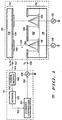
- FIG.1 is a schematic representation of a field emission display (FED) 100 in accordance with a preferred embodiment of the invention.
- FED 100 includes an FED device 110 and a control circuit 111 for controlling emission current.
- FED device 110 includes a cathode plate 112 and an anode plate 114.
- Cathode plate 112 includes a substrate 116, which can be made from glass, silicon, and the like.
- a first column electrode 118 and a second column electrode 120 are disposed upon substrate 116.
- First column electrode 118 is connected to a first voltage source 130, V 1
- second column electrode 120 is connected to a second voltage source 132, V 2 .
- a dielectric layer 122 is disposed upon column electrodes 118, 120, and further defines a plurality of wells.
- An electron emitter structure 124 such as a Spindt tip, is disposed in each of the wells.
- Anode plate 114 is disposed to receive an emission current 134, which is defined by the electrons emitted by electron emitter structures 124.
- a gate extraction electrode 126 is formed on dielectric layer 122 and is spaced apart from and is proximate to electron emitter structures 124. Column electrodes 118, 120 and gate extraction electrode 126 are used to selectively address electron emitter structures 124.
- FIG.1 depicts only a couple of column electrodes and one gate extraction electrode. However, it is desired to be understood that any number of column and gate extraction electrodes can be employed.
- An exemplary number of gate extraction electrodes for an FED device is 240, and an exemplary number of column electrodes is 960.
- Methods for fabricating cathode plates for matrix-addressable field emission displays are known to one of ordinary skill in the art.
- Anode plate 114 includes a transparent substrate 136 made from, for example, glass.
- An anode 138 is disposed on transparent substrate 136.
- Anode 138 is preferably made from a transparent conductive material, such as indium tin oxide.
- anode 138 is a continuous layer that opposes the entire emissive area of cathode plate 112. That is, anode 138 preferably opposes the entirety of electron emitter structures 124.
- An input 142 of anode 138 is designed to be connected to an output of a power supply 146.
- Power supply 146 includes one of several types of power supplies, such as a stepping-up transformer, a piezo electric power supply, and the like.
- power supply 146 is a variable, high-voltage power supply, which can provide an anode voltage, V A , on the order of 5000 volts.
- An anode current 144, I A flows from power supply 146 to anode 138.
- a useful assumption is that the magnitude of anode current 144 is equal to the magnitude of emission current 134.
- a plurality of phosphors 140 is disposed upon anode 138.
- Phosphors 140 are cathodoluminescent.
- phosphors 140 emit light upon activation by emission current 134.
- Methods for fabricating anode plates for matrix-addressable field emission displays are also known to one of ordinary skill in the art.
- control circuit 111 includes a sensor 150.
- An input of sensor 150 is connected to power supply 146.
- An output signal 148 flows from power supply 146 to sensor 150.
- Output signal 148 contains information corresponding to the operating parameters of power supply 146.
- output signal 148 can contain information about the electrical current, power output, or duty cycle of power supply 146.
- emission current 134 or anode current 144 is measured directly, as by making a current measurement, or indirectly.
- Indirect detection entails extraction of information about emission current 134 from the measured operating parameter of power supply 146.
- the power output of power supply 146 is proportional to anode current 144 and, correspondingly, emission current 134.
- Sensor 150 is responsive to output signal 148 and generates an output signal 152, which is useful for activating a current controller 154.
- Output signal 152 also contains information corresponding to an operating parameter of power supply 146.
- Current controller 154 has an output connected to an input of a gate voltage source 158.
- An output of gate voltage source 158 is connected to an input 128 of gate extraction electrode 126.
- current controller 154 In response to output signal 152 of sensor 150, current controller 154 generates an output signal 156.
- Output signal 156 manipulates gate voltage source 158 to adjust a gate voltage, V G , at gate extraction electrode 126. The gate voltage is adjusted by an amount sufficient to cause emission current 134 and, correspondingly, anode current 144 to reach a set point, desired value.
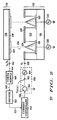
- FIG.2 is a schematic representation of FED 100 having current controller 154 that manipulates an offset voltage source 160, in accordance with the claims.
- the gate voltage source 158 includes offset voltage source 160 and a scanning voltage source 164.
- Offset voltage source 160 has an input for receiving output signal 156 of current controller 154. To adjust the gate voltage in accordance with the invention, output signal 156 manipulates offset voltage source 160.
- Offset voltage source 160 provides an offset voltage, V OFFSET , at an output 162.
- Scanning voltage source 164 is useful for adding a scanning voltage, V S , to the offset voltage.
- Offset voltage source 160 and scanning voltage source 164 are operably connected to achieve the addition of the offset and scanning voltages.
- offset voltage source 160 is connected in series with scanning voltage source 164, such that output 162 of offset voltage source 160 is connected to a negative input of scanning voltage source 164.
- Scanning voltage source 164 is activated to provide the scanning voltage by control circuitry (not shown).
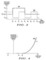
- FIG.3 is a timing diagram illustrating a method for operating FED 100 during the display mode of operation of FED 100.
- the display mode of operation is characterized by the creation of a display image at anode plate 114.
- Represented in FIG.3 is the selective addressing of electron emitter structure 124 at the intersection of gate extraction electrode 126 and first column electrode 118.
- FIG.3 illustrates a graph 166 of gate voltage and a graph 168 of column voltage, V 1 , at first column electrode 118.
- the column voltage is equal to V 1,1 and the gate voltage is equal to V OFFSET,1 . Because the gate voltage is less than the column voltage, no electron emission occurs.
- scanning voltage source 164 is activated, such that a scanning voltage is added to V OFFSET,1, resulting in a gate voltage of V G,1 .
- gate extraction electrode 126 is being scanned. That is, electron emitter structures 124 that are located along gate extraction electrode 126 can be caused to emit if an appropriate potential is applied to the corresponding column electrodes.
- electron emitter structure 124 at first column electrode 118 is caused to emit between times to and t 2 by applying a column voltage of V 1,2 . That is, the potential difference, ⁇ V, between the column voltage and the gate voltage is sufficiently large to cause electron emission of a desired value.
- the column voltage is returned to V 1,1 , resulting in a ⁇ V that is insufficient to cause emission, and electron emission ceases.
- the scanning of gate extraction electrode 126 is terminated by deactivating scanning voltage source 164, so that the gate voltage returns to the offset value.
- anode voltage, V A is selected to provide a desired brightness level for the light output from anode plate 114.
- an operating anode voltage, V A,OP on the order of thousands of volts can be employed.
- FIG.4 illustrates a graph 169 of emission current versus potential difference, ⁇ V, between the column voltage and the gate voltage, and further indicates operating points corresponding to various times represented in FIG.3.
- emission current 134 is activated, whereas at times t 3 , t 5 , and t 7 , electron emission is negligible.
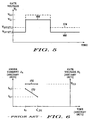
- FIG.5 illustrates graph 166 of FIG.3 and a graph 174 of the gate voltage before and after, respectively, a step of adjusting the gate voltage to control the emission or anode current in accordance with the invention.
- the offset voltage is initially set at V OFFSET,1 .
- gate extraction electrode 126 is scanned, the scanning voltage is added, resulting in a gate voltage of V G,1 .
- the gate voltage is adjusted in accordance with the invention. If emission current 134 has decreased, the adjusted gate voltage, as indicated by graph 174, is greater than the initial gate voltage. During the adjustment, the offset voltage is increased to V OFFSET,2 . Subsequently, when gate extraction electrode 126 is scanned, the constant scanning voltage is added to the adjusted offset voltage, increasing the gate voltage to V G,2 .
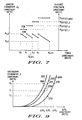
- FIG.6 illustrates a graph 170 of gate voltage and a graph 172 of anode current for a prior art method of operating a field emission display.
- the gate voltage remains constant at V G,0 over the operating lifetime of the display.
- the anode current which corresponds to the emission current, is not controlled, so that it decreases continuously during the operating lifetime of the display, as indicated by graph 172.
- Operation of the prior art FED starts at time t 0 .
- the prior art display lifetime, t' LIFE is defined as the total operating time required for the anode current to reach a selected value, I A,f .
- the value of I A,f is typically expressed as a percentage of an initial anode current, I A,0 , such as 50% of I A,0 .
- FIG.7 illustrates a graph 176 of anode current 144 and a graph 178 of offset voltage, in accordance with the method of the invention.
- the abscissa represents operating time, during which FED 100 is in a display mode of operation.
- illustrated in FIG.7 are at least four periods of operation of FED 100.
- the times specifically indicated on the abscissa in FIG.7 do not necessarily correspond to times specifically indicated in the other figures of the description.
- control method of the invention is performed at each start up of FED 100, just prior to a period of operation.
- the initial value, I A,0 , and final value, I A,f , of anode current 144 in FIG.7 are selected to be equal to those of FIG.6.
- Operation of FED 100 begins at time t 0 .
- a period of operation also begins at each of times t 1 , t 2 , and t 3 .
- Further shown at times t 1 , t 2 , and t 3 are the values of anode current 144 and offset voltage existing prior to and following control of the emission current, in accordance with the invention.
- the lower point on graph 176 indicates the value of anode current 144 at the end of the first period of operation.
- the method of the invention is employed to adjust the offset voltage from V OFFSET, 1 TO V OFFSET,2 .
- the adjusted offset voltage causes anode current 144 to return to the set point, which is the initial value, I A,0 , of anode current 144.
- the operating lifetime, t LIFE , of FED 100 is determined by a maximum offset voltage, V OFFSET,MAX , and by the lower limit, I A,f , of anode current 144.
- the maximum offset voltage can be defined by the operating limits of offset voltage source 160.
- the maximum offset voltage can equal a maximum voltage provided by offset voltage source 160.
- the maximum offset voltage may be defined by limits placed upon switching power requirements or by driver limitations.
- the operating lifetime includes the time, t 3 , required to reach the maximum offset voltage, V OFFSET,MAX .
- the operating lifetime further includes the operating time (t LIFE - t 3 ) required for anode current 144 to reach the selected, final value, I A,f , while FED 100 operates at a constant offset voltage of V OFFSET,MAX .
- the slopes of the segments of graph 176 are depicted in FIG.7 as being equal. However, they may differ. Also, the difference in anode current (graph 176) between consecutive operating periods, represented at times t 1 , t 2 , and t 3 , is depicted as being constant. However, the difference in anode current may vary. Furthermore, the duration of each operating period is not necessarily the same.
- t' LIFE the lifetime of the prior art represented in FIG.6.
- the method of the invention provides an appreciably improved display operating lifetime, t LIFE , over that of the prior art.
- the realized improvement in lifetime may not be equal to that shown in FIG.7.
- adjustment of the gate voltage in accordance with the invention can occur at each start-up of the display.
- the scope of the invention is not limited to this particular timing scheme.
- the steps of the invention can be performed at the end of selected display frames, during blanking intervals.
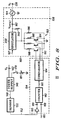
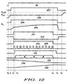
- FIG.8 is a circuit diagram of control circuit 111, in accordance with the preferred embodiment of the invention.
- current controller 154 includes a counter 182 and a comparator 184
- offset voltage source 160 includes a variable resistor 193 and a regulator 200, which is connected in parallel to a resistor 202.
- Control circuit 111 of FIG.8 further includes an electric relay 179 and a variable resistor 181, which are useful for adjusting the anode voltage, V A .
- Electric relay 179 is connected, at a first terminal, to a feedback circuit (not shown) of power supply 146 and, at a second terminal, to variable resistor 181.
- Electric relay 179 is controlled by a signal (not shown), which causes electric relay 179 to make or break the connection between power supply 146 and variable resistor 181.
- a first input 186 of counter 182 is connected to the output of sensor 150.
- the output of counter 182 is connected to an input of comparator 184, and outputs 192 of comparator 184 are connected to inputs of variable resistor 193.
- sensor 150 is a pulse modulator, such as a pulse width modulator and/or a pulse frequency modulator.
- Output signal 152 is a digital signal.
- the width and frequency of the pulses encode information corresponding to the operating parameters of power supply 146. That is, output signal 152 is a function of, for example, time, temperature, output power, and/or duty cycle.
- Output signal 152 is transmitted to first input 186 of counter 182.
- a buffer 195 is connected to first input 186 of counter 182 to minimize the loading of output signal 152.
- First input 186 is connected to the clock of counter 182.
- Counter 182 has a second input 188, which is connected to the clock enabler of counter 182.
- Second input 188 is designed to receive a counter enabler signal 180.
- Counter 182 generates an output signal 190, which is a data signal including N bits.
- Variable resistor 193 includes a plurality of resistors 198, 196, which are connected in parallel. The resistance of each of resistors 198, 196 is individually selected and need not be equal to the same value. Each of resistors 198 is further connected in series to a transistor 194, which performs a switching function to allow control of current flow through resistors 198. The base of each transistor 194 is connected to one of outputs 192 of comparator 184. Comparator 184 controls the effective resistance of variable resistor 193 by controlling the operational status of transistors 194.
- Regulator 200 is an adjustable linear regulator.
- V OFFSET V b (R 2 /R effective ), where:
- Equations (1) and (2) show that, as resistors 198 are effectively added by comparator 184, the effective resistance of variable resistor 193 falls, and the offset voltage increases.
- Comparator 184 utilizes the information provided by output signal 190 to determine the required adjustment of the offset voltage.
- the offset voltage is determined by the effective resistance of variable resistor 193.
- comparator 184 performs the function of enabling the required effective resistance of variable resistor 193.
- the step of adjusting the gate voltage can be achieved by mapping a detected value of emission current 134 into a set point value to define the adjusted gate voltage.
- the mapping operation utilizes the detected value of emission current 134 to arrive at a configuration for variable resistor 193, which will produce the adjusted offset voltage.
- the mapping operation can be implemented using a look-up table. The information in the look-up table is generated by employing a mapping function.
- Formulation of the mapping function requires information about the relationship between emission current 134 and the gate voltage. For example, a useful approximation is that emission current 134 is proportional to the offset voltage. Alternatively, a more precise relationship can be determined for a given display design, by using empirical methods or computer simulations, and can be utilized as described in greater detail with reference to FIG.9.
- Formulation of the mapping function further requires information about the relationship between emission current 134 and anode voltage.
- emission current varies with anode voltage.
- the anode voltage is preferably not constant throughout the control and display modes of operation of FED 100.
- anode voltage, V A at anode 138 preferably equals a control value, V A,C .
- the anode voltage is equal to operating anode voltage, V A,OP .
- the control value, V A,C is less than operating anode voltage, V A,OP .
- the control value is selected to reduce or eliminate emission of visible light at anode plate 114 during the control mode of operation, whereas the operating anode voltage is selected to provide a display image having a particular level of brightness.
- the set point value of emission current 134 during the control mode of operation does not equal the desired value of emission current 134 selected for the display mode of operation. Rather, the set point value for the control mode is selected to take into account the effect upon emission current 134 of the increase in the anode voltage, when FED 100 enters the display mode of operation.
- FIG.9 is a family of operating curves 201, 203, 205, of emission current, I, versus potential difference, ⁇ V, (between column voltage and gate voltage) for FED 100 at a constant temperature.
- FIG.9 further illustrates a mapping function for mapping a measured operating point into an operating point having an emission current equal to the set point value, in accordance with the method of the invention.
- the operating curve of FED 100 changes with respect to operating time due to the contamination of electron emitter structures 124. That is, chemical alteration of the emissive surfaces results in alteration of the work function of the surface and, therefore, produces a shift in the operating curve.
- First operating curve 201 of FIG.9 is the initial operating curve of FED 100.
- Second operating curve 203 is the operating curve at the time of a first detection and adjustment of emission current 134, in accordance with the method of the invention.
- Third operating curve 205 is the operating curve of FED 100 at the time of a second detection and adjustment of emission current 134, in accordance with the method of the invention.
- FED 100 operates at a first operating point 199 on first operating curve 201; emission current 134 is equal to I 0 , which is the desired value, and ⁇ V is equal to ⁇ V 0 .
- the value of emission current 134 decreases due to, for example, contamination of electron emitter structures 124.
- the value of emission current 134 is detected at a value of I 1 , and ⁇ V remains unchanged at a value of ⁇ V 0 , so that FED 100 operates at a second operating point 209. Determination of the operating point allows identification of the operating curve, which is second operating curve 203 in this example.
- the required ⁇ V can be found.
- the required ⁇ V is found by identifying the operating point along the operating curve that includes an emission current equal to I 0 , the desired value. In this manner, a third operating point 211 is selected along second operating curve 203, and the required value of ⁇ V is found to be ⁇ V 1 . Because the values of ⁇ V, scanning voltage, and column voltage are known, the required offset voltage can be calculated. The required effective resistance of variable resistor 193 can then be determined.
- the mapping function is similarly utilized to calculate the required offset voltage for use during the third operating period, as further illustrated in FIG.9.
- the value of emission current 134 is detected at a value of I 2
- ⁇ V is at a value of ⁇ V 1
- FED 100 operates at a fourth operating point 213, which is on third operating curve 205.
- a fifth operating point 215 is the operating point on third operating curve 205 that includes the desired emission current, I 0 .
- the required value of ⁇ V for the third operating period is therefore ⁇ V 2 .
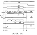
- FIG.10 is a timing diagram of the operation of the embodiment of FIG.8, in accordance with the method of the invention.
- power supply 146 is powered up, as represented by a graph 191 in FIG.10.
- Output signal 148 is represented by a graph 204 in FIG.10.
- output signal 148 is an alternating current (A.C.) signal corresponding to the power output of power supply 146.
- A.C. alternating current
- the pulse modulator of sensor 150 produces output signal 152, which is represented by a graph 206 in FIG.10.
- the anode voltage, V A at anode 138 (FIG.1) is ramped up to control value, V A,C , as illustrated in a graph 208 of FIG.10.
- the anode voltage is increased to operating anode voltage, V A,OP , as illustrated by graph 208 at time t 4 .
- the value of the anode voltage is determined by the configuration of electric relay 179 and variable resistor 181 (FIG.8). During the control mode of operation, electric relay 179 is caused to break the connection between power supply 146 and variable resistor 181. This configuration of electric relay 179 is represented by a graph 217 for times less than time t 4 . Graph 217 further shows that, at time t 4 , electric relay 179 is caused to make a connection between power supply 146 and variable resistor 181. The value of the anode voltage (V A,OP ) for times greater than t 4 is determined by the value of the resistance of variable resistor 181.
- counter enabler signal 180 is fed to second input 188, for enabling counter 182, as represented by a graph 210 in FIG.10.
- counter 182 When enabled, counter 182 generates the counter bits of output signal 190, as illustrated by a graph 212.
- the offset voltage which is represented by a graph 216, is set to an initial value, which can be a default setting or the value that was used during a period of operation immediately prior to the current control sequence.
- the offset voltage is applied to all gate extraction electrodes of FED 100.
- the scanning voltage is also applied to all gate extraction electrodes of the array by circuitry (not shown). Emission-activating potentials are applied to all column electrodes of FED 100. In this manner at time t 2 , all of electron emitter structures 124 are caused to emit electrons, thereby defining emission. current 134, as represented by a graph 207 of FIG.10.
- all of electron emitter structures 124 in the array are caused to emit.
- the scope of the invention is not limited to this configuration; fewer than all of electron emitter structures 124 can be caused to emit.
- Activation of the entire array, or a substantial portion thereof, is beneficial for reducing signal errors that may be caused by electrical signal noise. That is, as the measured value of emission current 134 increases, the error due to signal noise decreases.
- Emission current 134 is then received at anode 138 (FIG.1). Generation of emission current 134 causes a change in output signal 148, as indicated by graph 204 at time t 2 .
- control circuit 111 measures emission current 134 and compares the measured value with a set point value.
- emission current 134 is measured by measuring a power output of power supply 146.
- the power output can be measured, for example, by measuring the duty cycle of power supply 146.
- comparator 184 activates an effective resistance of variable resistor 193, which adjusts the gate voltage in a manner sufficient to cause emission current 134 to approach the set point value. Most preferably, emission current 134 is caused to equal the set point value.
- comparator 184 activates selected ones of transistors 194, as represented by a graph 214 in Fig.10.
- the effective resistance of variable resistor 193 is decreased, causing an increase in the offset voltage, as illustrated by graph 216 at time t 3 .
- counter enabler signal 180 (graph 210) ceases the counting of counter 182. Also, electron emission, for the purpose of controlling emission current 134, is terminated, as indicated by graph 207 at time t 3 . Termination of emission by the array causes a change in output signal 148, as indicated by graph 204 at time t 3 .
- the anode voltage is increased to operating anode voltage, V A,OP , as illustrated by graph 208.
- the operating anode voltage is selected to provide a useful brightness level for creating the display image.
- the anode voltage is increased by causing electric relay 179 to make a connection between power supply 146 and variable resistor 181 (FIG.8), which is represented by graph 217 at time t 4 .
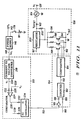
- FIG.11 is a circuit diagram of control circuit 111 for controlling emission current 134, in accordance with another embodiment of the invention.
- emission current 134 is measured by measuring a current, I PS , passing through power supply 146.
- the measured current can be a current passing through a secondary coil of a stepping-up transformer of power supply 146.
- output signal 148 from power supply 146 is a current signal.
- sensor 150 includes a current-to-voltage converter 218, a second comparator 224, and an oscillator 234.
- An input of current-to-voltage converter 218 is designed to be connected to power supply 146, and an output of current-to-voltage converter 218 is connected to a first input 222 of second comparator 224.
- a second input 226 of second comparator 224 is designed to receive a reference voltage signal 228.
- the output of second comparator 224 is connected to a first input 232 of oscillator 234.
- a second input 236 of oscillator 234 is connected to a reset and is designed to receive a reset signal 238.
- the output of oscillator 234 is connected to first input 186 of counter 182 of current controller 154.
- the circuitry of current controller 154 and gate voltage source 158 is described with reference to FIG.8.
- FIG.12 is a timing diagram of the operation of the embodiment of FIG.11, in accordance with the method of the invention.
- power supply 146 is powered up, as represented by graph 191 in FIG.12.
- the anode voltage is ramped up to control value, V A,C , as illustrated by graph 208.
- the offset voltage is equal to an initial value, which can be a default setting or the value that was used during a period of operation immediately prior to the current control sequence.
- the offset voltage is applied to all of the gate extraction electrodes of FED 100.
- the scanning voltage is also applied to all of the gate extraction electrodes of the array by circuitry (not shown).
- Emission-activating potentials are applied to all of the column electrodes of FED 100.
- all of electron emitter structures 124 are caused to emit electrons, thereby defining emission current 134.
- graph 207 of FIG.12 electron emission commences at time t 1 .
- Emission current 134 is then received at anode 138 (FIG.1).
- Output signal 148 is represented by graph 204. At time t1, output signal 148 changes in response to the generation of emission current 134.
- Output signal 148 from power supply 146 is transmitted to current-to-voltage converter 218, which includes circuitry useful for converting the current signal of output signal 148 to a corresponding voltage signal 220.
- current-to-voltage converter 218 can be a simple resistor.
- the value, V I , of voltage signal 220 is represented by a graph 240 in FIG.12. The control of V I commences at time t 3 , at which time current controller 154 is activated, in the manner described with reference to FIGs.8 and 10.
- reference voltage signal 228 is applied to second input 226 of second comparator 224, as represented by a graph 241 in FIG.12.
- a set point value, V C , of reference voltage signal 228 corresponds to the desired value of emission current 134 during the control mode of operation.
- reset signal 238 is applied to second input 236 of oscillator 234, as shown by a graph 242 in FIG.12.
- Second comparator 224 compares the value, V I , of voltage signal 220 with set point value, V C , of reference voltage signal 228. As long as V C is greater than V I , an output signal 230 of second comparator 224 defines an enabling signal, which activates the clock enabler of oscillator 234. Between times t 2 and t 4 , V I is less than V C , and output signal 230 is activated to its enabling state, as shown by a graph 244.
- Oscillator 234 is responsive to output signal 230 of second comparator 224 and generates output signal 152, which is represented by a graph 246 in FIG.12.
- counter enabler signal 180 enables counter 182, as shown by graph 210.
- counter 182 In response to output signal 152 of sensor 150, counter 182 generates output signal 190, which is represented by graph 212 in FIG.12.
- Comparator 184 and gate voltage source 158 function in a manner similar to that described with reference to FIGs.8 and 10, resulting in the adjustment of the effective resistance of variable resistor 193, as illustrated by a graph 248 in FIG.12. As the effective resistance is reduced, the offset voltage increases, as shown by graph 250.
- the set point value of reference voltage signal 228 is removed from second comparator 224 (graph 241). Electron emission by the array of electron emitter structures is thereafter terminated at time t 5 (graph 207), which causes a change in output signal 148 (graph 204) and further causes the value of V I to drop (graph 240). At time t 6 , the anode voltage (graph 208) is ramped up to the operating anode voltage, V A,OP , in the manner described with reference to FIG.10.
- the invention is for a method and a field emission display useful for maintaining a constant emission current over the lifetime of the display.
- the method of the invention includes a step for manipulating a gate voltage to cause an emission current to equal a set point value.
- a field emission display in accordance with the claims includes a control circuit for controlling the emission current at start-up.
- the method and display of the invention provide the benefits of constant brightness and an improved display operating lifetime compared to operation at a constant gate voltage.
- the step of mapping a measured value of emission current into a set point value can include using operating curves that take into account the effects of variation in temperature.
- the second comparator can include a low-pass filter circuit.
- the emission current can be measured by measuring the anode current at the input to the anode.
Claims (9)
- Verfahren zum Steuern eines Emissionsstroms (134) in einem Feldemissionsdisplay (100), das eine Mehrzahl von elektronenemittierenden Strukturen (124), eine Gate-Extraktionselektrode (126) und eine Anode (138) hat, wobei das Verfahren die folgenden Schritte umfasst:dadurch gekennzeichnet, dass,Bewirken, dass die Mehrzahl von elektronenemittierenden Strukturen (124) Elektronen emittieren, wodurch der Emissionsstrom (134) definiert wird;Messen des Emissionsstroms (134), wodurch ein gemessener Wert definiert wird;Vergleichen des gemessenen Wertes mit einem Sollwert; undAnlegen einer Gate-Spannung einschließlich einer Offset-Spannung an der Gate-Extraktionselektrode (126),
wenn der gemessene Wert nicht gleich dem Sollwert ist, die Gate-Spannung durch Einstellen der Offset-Spannung in einer Weise eingestellt wird, die ausreichend ist, um zu verursachen, dass sich der Emissionsstrom (134) dem Sollwert annähert. - Verfahren zum Steuern eines Emissionsstroms (134) in einem Feldemissionsdisplay (100) nach Anspruch 1, bei dem der Schritt des Messens des Emissionsstroms (134) die Schritte des Empfangens des Emissionsstroms (134) an der Anode (138), wodurch ein Anodenstrom (144) definiert wird, und das Messen des Anodenstroms (144) umfasst.
- Verfahren zum Steuern eines Emissionsstroms (134) in einem Feldemissionsdisplay (100) nach Anspruch 1, bei dem das Feldemissionsdisplay (100) durch eine Anodenbetriebsspannung gekennzeichnet ist, und wobei es weiterhin, gleichzeitig mit dem Schritt des Verursachens, dass die Mehrzahl von elektronenemittierenden Strukturen (124), Elektronen emittiert, den Schritt des Bereitstellens einer ersten Anodenspannung an der ersten Anode (138) umfasst, wobei die erste Anodenspannung geringer ist als die Anodenbetriebsspannung.
- Verfahren zum Steuern eines Emissionsstroms (134) in einem Feldemissionsdisplay (100) nach Anspruch 1, das weiterhin den Schritt des Verbindens der Anode (138) mit der Stromversorgung (146) umfasst und bei dem der Schritt des Messens des Emissionsstroms (134) die Schritte des Empfangens des Emissionsstroms (134) an der Anode und des Messens einer Leistungs- bzw. Energie- bzw. Spannungsausgabe der Stromversorgung (146) umfasst.
- Verfahren zum Steuern eines Emissionsstroms (134) in einem Feldemissionsdisplay (100) nach Anspruch 1, bei dem der Schritt des Einstellens der Gate-Spannung den Schritt des Einstellens der Gate-Spannung in einer Weise umfasst, die ausreicht, um zu verursachen, dass der Emissionsstrom (134) gleich dem Sollwert ist.
- Verfahren zum Steuern eines Emissionsstroms (134) in einem Feldemissionsdisplay (100) nach Anspruch 1, bei dem der Schritt des Einstellens der Gate-Spannung die Schritte des Abbildens des gemessenen Wertes in den Sollwert, um eine eingestellte Gate-Spannung zu definieren, und des Zuführens der eingestellten Gate-Spannung zu der Gate-Extraktionselektrode (126) umfasst.
- Feldemissionsdisplay (100), das folgendes umfasst:eine Kathodenplatte (112), die eine Mehrzahl von elektronenemittierenden Strukturen (124) und eine Gate-Extraktionselektrode (126) hat, die getrennt von der Mehrzahl der elektronenemittierenden Strukturen (124) angeordnet ist;eine Anodenplatte (114), die geeignet ist, Elektronen zu empfangen, die durch die Mehrzahl von elektronenemittierenden Strukturen (124) emittiert werden, und die eine Anode (138) hat, wobei die Anode (138) geeignet ist, mit einer Stromversorgung (146) verbunden zu werden;einen Sensor (150), der einen Eingang und einen Ausgang hat, wobei der Eingang geeignet ist, mit der Stromversorgung (146) verbunden zu werden; undeine Stromsteuerung (154), die einen Eingang (152) und einen Ausgang (156) hat, wobei der Eingang der Stromsteuerung (154) mit dem Ausgang des Sensors (150) verbunden ist, gekennzeichnet durch;eine Gate-Spannungsquelle (158) einschließlich einer Offset-Spannungsquelle (160), wobei die Gate-Spannungsquelle (158) einen Eingang und einen Ausgang hat, wobei der Eingang der Gate-Spannungsquelle (158) mit dem Ausgang der Stromsteuerung (154) verbunden ist, und wobei der Ausgang der Gate-Spannungsquelle (158) mit der Gate-Extraktionselektrode (126) verbunden ist, so dass die Offset-Spannungsquelle (160) mit dem Stromsteuerausgang (156) verbunden ist, um die Gate-Spannung in einer Weise einzustellen, die ausreichend ist, um zu verursachen, dass sich der Emissionsstrom dem Sollwert annähert.
- Feldemissionsdisplay (100) nach Anspruch 7, wobei die Gate-Spannungsquelle (158) einschließlich der Offset-Spannungsquelle weiterhin eine Abtastspannungsquelle umfasst, wobei die Offset-Spannungsquelle mit der Abtastspannungsquelle in Wirkverbindung steht, so dass die Abtastspannungsquelle, wenn sie aktiviert wird, einer durch die Offset-Spannungsquelle zur Verfügung gestellten Offset-Spannung eine Abtastspannung hinzufügt.
- Feldemissionsdisplay (100) nach Anspruch 7, wobei der Sensor (150) einen Strom-Spannungs-Wandler (218), der einen Eingang und einen Ausgang hat, einen Komparator (184), der erste und zweite Eingänge hat, und einen Oszillator (234) umfasst, der einen Eingang und einen Ausgang hat, wobei der Eingang des Strom-Spannungs-Wandlers (218) geeignet ist, mit der Stromversorgung (146) verbunden zu werden, wobei der Ausgang des Strom-Spannungs-Wandlers (218) mit dem ersten Eingang des Komparators (184) verbunden ist, wobei der zweite Eingang des Komparators (184) geeignet ist, ein Spannungsnachschlagesignal zu empfangen, wobei der Ausgang des Komparators (184) mit dem Eingang des Oszillators (234) verbunden ist, wobei der Ausgang des Oszillators (234) mit dem Eingang der Stromsteuerung (154) verbunden ist.
Applications Claiming Priority (3)
| Application Number | Priority Date | Filing Date | Title |
|---|---|---|---|
| US253100 | 1994-06-02 | ||
| US09/253,100 US6060840A (en) | 1999-02-19 | 1999-02-19 | Method and control circuit for controlling an emission current in a field emission display |
| PCT/US2000/003122 WO2000049636A1 (en) | 1999-02-19 | 2000-02-07 | Method and circuit for controlling field emission current |
Publications (2)
| Publication Number | Publication Date |
|---|---|
| EP1155432A1 EP1155432A1 (de) | 2001-11-21 |
| EP1155432B1 true EP1155432B1 (de) | 2004-05-06 |
Family
ID=22958853
Family Applications (1)
| Application Number | Title | Priority Date | Filing Date |
|---|---|---|---|
| EP00906002A Expired - Lifetime EP1155432B1 (de) | 1999-02-19 | 2000-02-07 | Verfahren und schaltungsanordnung zur steuerung von feldemissionsstrom |
Country Status (6)
| Country | Link |
|---|---|
| US (1) | US6060840A (de) |
| EP (1) | EP1155432B1 (de) |
| JP (1) | JP2002537588A (de) |
| DE (1) | DE60010434T2 (de) |
| TW (1) | TW451256B (de) |
| WO (1) | WO2000049636A1 (de) |
Families Citing this family (38)
| Publication number | Priority date | Publication date | Assignee | Title |
|---|---|---|---|---|
| US6462484B2 (en) * | 1998-08-31 | 2002-10-08 | Candescent Intellectual Property Services | Procedures and apparatus for turning-on and turning-off elements within a field emission display device |
| JP4505868B2 (ja) * | 1999-03-12 | 2010-07-21 | 双葉電子工業株式会社 | 電界放出型表示装置の輝度補償回路 |
| JP2001209352A (ja) * | 2000-01-24 | 2001-08-03 | Nec Corp | 電界電子放出型ディスプレィ装置およびその駆動方法 |
| US6392355B1 (en) | 2000-04-25 | 2002-05-21 | Mcnc | Closed-loop cold cathode current regulator |
| US6404136B1 (en) * | 2000-07-05 | 2002-06-11 | Motorola Inc. | Method and circuit for controlling an emission current |
| US6346776B1 (en) * | 2000-07-10 | 2002-02-12 | Memsolutions, Inc. | Field emission array (FEA) addressed deformable light valve modulator |
| US6559819B1 (en) | 2000-07-17 | 2003-05-06 | Motorola, Inc. | Method for extending an operating range of a field emission display and circuit therefor |
| US6542136B1 (en) | 2000-09-08 | 2003-04-01 | Motorola, Inc. | Means for reducing crosstalk in a field emission display and structure therefor |
| US6600464B1 (en) | 2000-09-08 | 2003-07-29 | Motorola, Inc. | Method for reducing cross-talk in a field emission display |
| TWM309746U (en) * | 2000-10-19 | 2007-04-11 | Matsushita Electric Ind Co Ltd | Driving apparatus for a field emission device, field emission device, electron source, light source, image display apparatus, electron gun, electron beam apparatus, cathode ray tube, and discharge tube |
| JP2008052289A (ja) * | 2001-09-07 | 2008-03-06 | Semiconductor Energy Lab Co Ltd | 発光装置及び電子機器 |
| US7088052B2 (en) * | 2001-09-07 | 2006-08-08 | Semiconductor Energy Laboratory Co., Ltd. | Light emitting device and method of driving the same |
| KR100500777B1 (ko) * | 2001-09-21 | 2005-07-12 | 엘지전자 주식회사 | 평면형 전계방출 표시소자의 구동장치 |
| US6911781B2 (en) * | 2002-04-23 | 2005-06-28 | Semiconductor Energy Laboratory Co., Ltd. | Light emitting device and production system of the same |
| US7158102B2 (en) * | 2002-04-26 | 2007-01-02 | Candescent Technologies Corporation | System and method for recalibrating flat panel field emission displays |
| JP4266616B2 (ja) | 2002-11-13 | 2009-05-20 | キヤノン株式会社 | 表示装置及びその駆動制御方法 |
| JP3720017B2 (ja) * | 2002-11-14 | 2005-11-24 | 株式会社東芝 | 平面型表示装置を駆動する方法及び駆動システム |
| US6771027B2 (en) | 2002-11-21 | 2004-08-03 | Candescent Technologies Corporation | System and method for adjusting field emission display illumination |
| US20040100426A1 (en) * | 2002-11-21 | 2004-05-27 | Madhukar Gaganam | Field emission display brightness uniformity compensation system and method |
| FR2853133B1 (fr) * | 2003-03-27 | 2005-04-29 | Commissariat Energie Atomique | Dispositif et procede de commande et de controle d'une dose d'electrons emise par un micro-emetteur |
| KR100524772B1 (ko) * | 2003-04-18 | 2005-11-01 | 엘지전자 주식회사 | 전계 방출 소자의 에이징 구동 방법 |
| KR20050077972A (ko) * | 2004-01-30 | 2005-08-04 | 삼성에스디아이 주식회사 | 전계 방출 표시 장치 및 그 구동 방법 |
| US20070273617A1 (en) * | 2004-04-28 | 2007-11-29 | Hiroyuki Yamakawa | Field emission display and method for controlling the same |
| KR101022657B1 (ko) * | 2004-05-31 | 2011-03-22 | 삼성에스디아이 주식회사 | 전자 방출 장치의 구동방법 |
| KR20060001372A (ko) * | 2004-06-30 | 2006-01-06 | 삼성에스디아이 주식회사 | 배경휘도 저감형 전자 방출 장치 |
| KR20060104221A (ko) * | 2005-03-29 | 2006-10-09 | 삼성에스디아이 주식회사 | 전자 방출 표시장치 및 그 제어 방법 |
| KR20060122475A (ko) * | 2005-05-27 | 2006-11-30 | 삼성에스디아이 주식회사 | 전자방출표시장치 및 그 전압제어방법 |
| KR20070029020A (ko) * | 2005-09-08 | 2007-03-13 | 삼성에스디아이 주식회사 | 전자방출표시소자 및 그의 구동방법 |
| KR20070043543A (ko) * | 2005-10-21 | 2007-04-25 | 삼성에스디아이 주식회사 | 전자 방출 표시소자 및 그 제어 방법 |
| US20080150934A1 (en) * | 2006-12-01 | 2008-06-26 | Toshifumi Ozaki | Image display device |
| KR100863961B1 (ko) | 2007-08-02 | 2008-10-16 | 삼성에스디아이 주식회사 | 발광장치 및 이를 이용한 표시장치, 발광장치의 구동방법및 표시 장치의 구동방법 |
| JP2010019896A (ja) * | 2008-07-08 | 2010-01-28 | Canon Inc | 画像表示装置 |
| KR101104073B1 (ko) * | 2008-12-18 | 2012-01-12 | 한국전자통신연구원 | 전계 방출 장치 |
| US9646798B2 (en) | 2011-12-29 | 2017-05-09 | Elwha Llc | Electronic device graphene grid |
| US9171690B2 (en) | 2011-12-29 | 2015-10-27 | Elwha Llc | Variable field emission device |
| WO2013101948A1 (en) * | 2011-12-29 | 2013-07-04 | Elwha Llc | Materials and configurations of a field emission device |
| US9627168B2 (en) | 2011-12-30 | 2017-04-18 | Elwha Llc | Field emission device with nanotube or nanowire grid |
| WO2019151251A1 (ja) * | 2018-01-31 | 2019-08-08 | ナノックス イメージング ピーエルシー | X線管の制御方法及びx線管の制御装置 |
Family Cites Families (19)
| Publication number | Priority date | Publication date | Assignee | Title |
|---|---|---|---|---|
| US5157309A (en) * | 1990-09-13 | 1992-10-20 | Motorola Inc. | Cold-cathode field emission device employing a current source means |
| US5173634A (en) * | 1990-11-30 | 1992-12-22 | Motorola, Inc. | Current regulated field-emission device |
| US5262698A (en) * | 1991-10-31 | 1993-11-16 | Raytheon Company | Compensation for field emission display irregularities |
| DE69320590T2 (de) * | 1992-11-02 | 1999-03-04 | Motorola Inc | Helligkeitsmodulierte Kaltkathodeanzeigevorrichtung |
| US5313140A (en) * | 1993-01-22 | 1994-05-17 | Motorola, Inc. | Field emission device with integral charge storage element and method for operation |
| US5404081A (en) * | 1993-01-22 | 1995-04-04 | Motorola, Inc. | Field emission device with switch and current source in the emitter circuit |
| JPH0721903A (ja) * | 1993-07-01 | 1995-01-24 | Nec Corp | 電界放出型陰極を用いた陰極線管用電子銃構体 |
| US5514937A (en) * | 1994-01-24 | 1996-05-07 | Motorola | Apparatus and method for compensating electron emission in a field emission device |
| US5578906A (en) * | 1995-04-03 | 1996-11-26 | Motorola | Field emission device with transient current source |
| AU5777096A (en) * | 1995-06-12 | 1997-01-09 | Ecole Polytechnique Federale De Lausanne | Electron source and applications of the same |
| DE19522221A1 (de) * | 1995-06-20 | 1997-01-02 | Zeiss Carl Fa | Verfahren zur Regelung des Emissionsstromes einer Elektronenquelle und Elektronenquelle mit einer Regelung des Emissionsstromes |
| US5721560A (en) * | 1995-07-28 | 1998-02-24 | Micron Display Technology, Inc. | Field emission control including different RC time constants for display screen and grid |
| US5700175A (en) * | 1996-04-08 | 1997-12-23 | Industrial Technology Research Institute | Field emission device with auto-activation feature |
| JP2907150B2 (ja) * | 1996-09-27 | 1999-06-21 | 日本電気株式会社 | 冷陰極電子銃およびこれを用いた電子ビーム装置 |
| US5847515A (en) * | 1996-11-01 | 1998-12-08 | Micron Technology, Inc. | Field emission display having multiple brightness display modes |
| US5940052A (en) * | 1997-01-15 | 1999-08-17 | Micron Technology, Inc. | Current monitor for field emission displays |
| US5961362A (en) * | 1997-09-09 | 1999-10-05 | Motorola, Inc. | Method for in situ cleaning of electron emitters in a field emission device |
| US5910792A (en) * | 1997-11-12 | 1999-06-08 | Candescent Technologies, Corp. | Method and apparatus for brightness control in a field emission display |
| US5936354A (en) * | 1998-11-02 | 1999-08-10 | Motorola, Inc. | Field emission display with temperature sensing element and method for the operation thereof |
-
1999
- 1999-02-19 US US09/253,100 patent/US6060840A/en not_active Expired - Lifetime
-
2000
- 2000-02-07 DE DE60010434T patent/DE60010434T2/de not_active Expired - Fee Related
- 2000-02-07 WO PCT/US2000/003122 patent/WO2000049636A1/en active IP Right Grant
- 2000-02-07 EP EP00906002A patent/EP1155432B1/de not_active Expired - Lifetime
- 2000-02-07 JP JP2000600287A patent/JP2002537588A/ja not_active Withdrawn
- 2000-02-22 TW TW089102904A patent/TW451256B/zh not_active IP Right Cessation
Also Published As
| Publication number | Publication date |
|---|---|
| DE60010434D1 (de) | 2004-06-09 |
| JP2002537588A (ja) | 2002-11-05 |
| US6060840A (en) | 2000-05-09 |
| DE60010434T2 (de) | 2004-09-23 |
| TW451256B (en) | 2001-08-21 |
| WO2000049636A1 (en) | 2000-08-24 |
| EP1155432A1 (de) | 2001-11-21 |
Similar Documents
| Publication | Publication Date | Title |
|---|---|---|
| EP1155432B1 (de) | Verfahren und schaltungsanordnung zur steuerung von feldemissionsstrom | |
| US8279143B2 (en) | OLED luminance degradation compensation | |
| KR100412169B1 (ko) | 전계방출디바이스,전계방출디바이스화상표시장치,및전계방출디바이스에서전자방출을제어하는방법 | |
| US6404136B1 (en) | Method and circuit for controlling an emission current | |
| WO1999024961A1 (en) | Method and apparatus for brightness control in a field emission display | |
| EP1306870B1 (de) | Elektronenquelle des Feldemissionstyps und Verfahren zum Anlegen einer Vorspannung | |
| US7280088B2 (en) | Method and device for controlling a matrix electron source, with regulation by the emitted charge | |
| EP1729276A1 (de) | Elektronenemissionsanzeige und Verfahren zur Ansteuerung | |
| US6031344A (en) | Method for driving a field emission display including feedback control | |
| JP2001195026A (ja) | マトリクス型表示装置 | |
| US7696959B2 (en) | Display device and driving method of the same | |
| KR20080010873A (ko) | 발광소자 보정회로 및 보정방법 | |
| GB2105108A (en) | Aging electroluminescent devices | |
| US20060082317A1 (en) | Electron-emitting apparatus | |
| US6479938B1 (en) | Driving method for electric-field electron emission apparatus | |
| JP2006523858A (ja) | 表示装置 | |
| TW518627B (en) | Field emission display and method | |
| KR100805117B1 (ko) | 플라즈마 표시 장치 및 이에 사용되는 제어 장치 | |
| KR20020008254A (ko) | 액티브 소자의 구동 회로 및 제어 방법 | |
| JPH0782303B2 (ja) | 発光素子駆動装置 | |
| US20070146241A1 (en) | Method of Driving Field Emission Display | |
| KR100531794B1 (ko) | 표시 소자 제작용 잉크젯 프린터의 구동 장치 | |
| KR20010039027A (ko) | 전계 방출 표시장치 및 방법 | |
| KR19990066443A (ko) | 전계방출 디스플레이의 전류 제한 방법 및 장치 | |
| KR20050043477A (ko) | 표시 소자 제작용 잉크젯 프린터의 구동 장치 |
Legal Events
| Date | Code | Title | Description |
|---|---|---|---|
| PUAI | Public reference made under article 153(3) epc to a published international application that has entered the european phase |
Free format text: ORIGINAL CODE: 0009012 |
|
| 17P | Request for examination filed |
Effective date: 20010919 |
|
| AK | Designated contracting states |
Kind code of ref document: A1 Designated state(s): AT BE CH CY DE DK ES FI FR GB GR IE IT LI LU MC NL PT SE |
|
| RIN1 | Information on inventor provided before grant (corrected) |
Inventor name: FOO, KEN, KOK Inventor name: RAUMBAUGH, ROBERT, C. |
|
| 17Q | First examination report despatched |
Effective date: 20030407 |
|
| GRAP | Despatch of communication of intention to grant a patent |
Free format text: ORIGINAL CODE: EPIDOSNIGR1 |
|
| GRAS | Grant fee paid |
Free format text: ORIGINAL CODE: EPIDOSNIGR3 |
|
| GRAA | (expected) grant |
Free format text: ORIGINAL CODE: 0009210 |
|
| AK | Designated contracting states |
Kind code of ref document: B1 Designated state(s): DE FR GB |
|
| RIN1 | Information on inventor provided before grant (corrected) |
Inventor name: FOO, KEN, KOK Inventor name: RAUMBAUGH, ROBERT, C. |
|
| REG | Reference to a national code |
Ref country code: GB Ref legal event code: FG4D |
|
| REF | Corresponds to: |
Ref document number: 60010434 Country of ref document: DE Date of ref document: 20040609 Kind code of ref document: P |
|
| REG | Reference to a national code |
Ref country code: IE Ref legal event code: FG4D |
|
| ET | Fr: translation filed | ||
| PLBE | No opposition filed within time limit |
Free format text: ORIGINAL CODE: 0009261 |
|
| STAA | Information on the status of an ep patent application or granted ep patent |
Free format text: STATUS: NO OPPOSITION FILED WITHIN TIME LIMIT |
|
| 26N | No opposition filed |
Effective date: 20050208 |
|
| PGFP | Annual fee paid to national office [announced via postgrant information from national office to epo] |
Ref country code: FR Payment date: 20060202 Year of fee payment: 7 |
|
| PGFP | Annual fee paid to national office [announced via postgrant information from national office to epo] |
Ref country code: DE Payment date: 20060228 Year of fee payment: 7 |
|
| GBPC | Gb: european patent ceased through non-payment of renewal fee |
Effective date: 20070207 |
|
| REG | Reference to a national code |
Ref country code: FR Ref legal event code: ST Effective date: 20071030 |
|
| PG25 | Lapsed in a contracting state [announced via postgrant information from national office to epo] |
Ref country code: DE Free format text: LAPSE BECAUSE OF NON-PAYMENT OF DUE FEES Effective date: 20070901 |
|
| PG25 | Lapsed in a contracting state [announced via postgrant information from national office to epo] |
Ref country code: GB Free format text: LAPSE BECAUSE OF NON-PAYMENT OF DUE FEES Effective date: 20070207 Ref country code: FR Free format text: LAPSE BECAUSE OF NON-PAYMENT OF DUE FEES Effective date: 20070228 |
|
| PGFP | Annual fee paid to national office [announced via postgrant information from national office to epo] |
Ref country code: GB Payment date: 20060109 Year of fee payment: 7 |