EP1154525A2 - Double helix lead dressing of flat flexible cables - Google Patents
Double helix lead dressing of flat flexible cables Download PDFInfo
- Publication number
- EP1154525A2 EP1154525A2 EP01401061A EP01401061A EP1154525A2 EP 1154525 A2 EP1154525 A2 EP 1154525A2 EP 01401061 A EP01401061 A EP 01401061A EP 01401061 A EP01401061 A EP 01401061A EP 1154525 A2 EP1154525 A2 EP 1154525A2
- Authority
- EP
- European Patent Office
- Prior art keywords
- double helix
- terminals
- cable
- flat
- cable assembly
- Prior art date
- Legal status (The legal status is an assumption and is not a legal conclusion. Google has not performed a legal analysis and makes no representation as to the accuracy of the status listed.)
- Granted
Links
Images

Classifications
-
- H—ELECTRICITY
- H01—ELECTRIC ELEMENTS
- H01R—ELECTRICALLY-CONDUCTIVE CONNECTIONS; STRUCTURAL ASSOCIATIONS OF A PLURALITY OF MUTUALLY-INSULATED ELECTRICAL CONNECTING ELEMENTS; COUPLING DEVICES; CURRENT COLLECTORS
- H01R12/00—Structural associations of a plurality of mutually-insulated electrical connecting elements, specially adapted for printed circuits, e.g. printed circuit boards [PCB], flat or ribbon cables, or like generally planar structures, e.g. terminal strips, terminal blocks; Coupling devices specially adapted for printed circuits, flat or ribbon cables, or like generally planar structures; Terminals specially adapted for contact with, or insertion into, printed circuits, flat or ribbon cables, or like generally planar structures
- H01R12/70—Coupling devices
- H01R12/71—Coupling devices for rigid printing circuits or like structures
- H01R12/72—Coupling devices for rigid printing circuits or like structures coupling with the edge of the rigid printed circuits or like structures
- H01R12/73—Coupling devices for rigid printing circuits or like structures coupling with the edge of the rigid printed circuits or like structures connecting to other rigid printed circuits or like structures
-
- H—ELECTRICITY
- H01—ELECTRIC ELEMENTS
- H01R—ELECTRICALLY-CONDUCTIVE CONNECTIONS; STRUCTURAL ASSOCIATIONS OF A PLURALITY OF MUTUALLY-INSULATED ELECTRICAL CONNECTING ELEMENTS; COUPLING DEVICES; CURRENT COLLECTORS
- H01R12/00—Structural associations of a plurality of mutually-insulated electrical connecting elements, specially adapted for printed circuits, e.g. printed circuit boards [PCB], flat or ribbon cables, or like generally planar structures, e.g. terminal strips, terminal blocks; Coupling devices specially adapted for printed circuits, flat or ribbon cables, or like generally planar structures; Terminals specially adapted for contact with, or insertion into, printed circuits, flat or ribbon cables, or like generally planar structures
- H01R12/70—Coupling devices
- H01R12/77—Coupling devices for flexible printed circuits, flat or ribbon cables or like structures
- H01R12/79—Coupling devices for flexible printed circuits, flat or ribbon cables or like structures connecting to rigid printed circuits or like structures
Definitions
- the present invention relates generally to electrical circuit module interconnecting cables and, more specifically, to an interconnecting cable utilizing a pair of flat cables adapted to form a self-supported interconnecting cable assembly.
- Flat flexible cables FFCs
- ribbon cables and other flat cabling technologies are well known in the electronics industry as a means of electrical systems interconnection.
- advantages provided by flat cables are simple, low cost systems assembly and ease in mass termination, since all the conductors of a flat cable are fixed in known relationship to one another in a flat, easy to handle, array.
- Such cables may be manufactured, for example, by coating and laminating operations or by etching or adhesive deposition techniques.
- Ribbon cables are typically terminated using insulation displacement connectors to form cable assemblies suitable for interconnecting printed circuit boards, circuit modules and other electrical and electronic devices.
- insulation displacement type connectors are relatively low, often resulting in inadvertent disassembly or disconnection. This condition may be somewhat remedied by the use of locking flight cable connectors.
- an adhesive is typically added to improve the retention force of the connector.
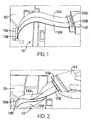
- FIG. 1 depicts a flat cable assembly.
- FIG. 1 depicts a printed circuit board (PCB) 105 connected to a circuit module 140 via a flat flexible cable (FFC) assembly (CA) comprising a pair of flat cables 130A and 130B having respective first or proximate terminating connectors 110A and 110B and respective second or distal terminating connectors 120A and 120B. That is, a first cable assembly is formed by connector 110A, FFC 130A and connector 120A, while a second cable assembly is formed by connector 110B, FFC 130B and connector 120B.
- PCB printed circuit board
- FFC assembly CA
- a first cable assembly is formed by connector 110A, FFC 130A and connector 120A
- a second cable assembly is formed by connector 110B, FFC 130B and connector 120B.
- the respective first terminating connectors 110A and 110B electronically and mechanically couple the ribbon cables 130A, 130B to the PCB 105, while the second terminating connectors 120A, 120B electronically and mechanically couple the ribbon cables 130A, 130B to the circuit module 140.
- the terminating connectors 110A, 110B, 120A and 120B comprise standard ribbon cable terminating connectors, such as insulation displacement-type connectors.
- the various electronic components are depicted on the PC board 105. Since the particular components depicted on the PC board 105 are not relevant to the subject invention, they will not be discussed in more detail. However, it is noted that the various electronic components may include electronic components that emit radio frequency (RF) signals or other electromagnetic radiation, or are effected by RF radiation or other electromagnetic radiation. As will be discussed in more detail below, the subject invention advantageously reduces the emissions of radio frequency and other electromagnetic emissions from the cable assembly.
- RF radio frequency
- FIG. 2 depicts the cable assembly of FIG. 1 as spatially modified according to an embodiment of the present invention. Specifically, FIG. 2 depicts the cable assembly of FIG. 1 comprising proximate connectors 110A and 110B, flat cables 130A and 130B, and respective distal connectors 120A and 120B. As previously noted, the cable assembly CA is proximally terminated at a printed circuit board 105 and distally terminated at a circuit module 140. Referring now to FIG. 2, the circuit module 140 is shown as having rotated by 180°, thereby causing a corresponding rotation of the flat cables 130A and 130B and respective distal terminations 120A and 120B as shown.
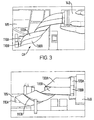
- FIG. 3 depicts the cable assembly of FIG. 2 as spatially modified according to an embodiment of the present invention. Specifically, FIG. 3 depicts the circuit module 140, and corresponding cable assembly CA of FIG. 2 rotated by an additional 180°, to provide thereby a full 360° of rotation with respect to the initially depicted cable assembly CA of FIG. 1.
- the double helix cable assembly structure has been formed. That is, the first 130A and second 130B flat cables have been adapted to form a double helix structure by rotating the distal connectors 120 by 360° with respect to the proximate connectors 110.
- each of the non-orthogonal proximate termination connectors may be considered as being in-line or generally in-line (parallel or generally parallel) and closely adjacent to the other non-orthogonal proximate termination connectors.
- the respective non-orthogonal distal terminating connectors are similarly positioned with respect to each other.
- FIG. 4 depicts the cable assembly of FIG. 3 mounted within an electronic apparatus. Specifically, FIG. 4 depicts the cable assemblies described above with respect to FIGS. 1-3 wherein the PCB 105 and circuit module 140 are secured within a common housing, thereby showing the actual use of a double helix cable assembly formed according to the present invention.
- FIG. 5 depicts a flow diagram of a method of forming a cable assembly according to the present invention. Specifically, FIG. 5 depicts a flow diagram of a method 500 suitable for use in, for example, a manufacturing or repair environment where the double helix assembly may be used.
- the method 500 is entered at step 510 and proceeds to step 520, where the length of the flat cable needed to provide the appropriate circuit interconnections is determined. That is, referring to box 515, parameters such as the end-to-end minimum length, the double helix minimum/maximum slack and any service "loop" is used to determine the length of the flat cables.
- the end-to-end minimum comprises the minimum distance between a proximate connector and distal connector within a cable assembly electrically coupling two circuits (e.g., between connectors 110 of PCB 105 and 120 of circuit module 140).
- the double helix minimum slack parameter comprises a length allowance for a minimum amount of slack within a double helix cable assembly configuration.
- the double helix maximum slack parameter comprises a length allowance for a maximum amount of slack within a double helix cable assembly configuration. It is noted that a length greater than a maximum slack parameter will result in a "droopy" double helix cable assembly, which may disadvantageously require additional securing means such as clamps to route properly between the two circuit connections.
- a "service loop" comprises a length allowance for accessing electrical components that are connected using the double helix cable assembly. The method 500 then proceeds to step 530.
- the basic flat cable assemblies are formed using the determined length. That is, each of the single or basic flat cable assemblies are formed using the length parameter determined at step 520.It must be noted that the basic flat cable assemblies may be formed using individual connectors or common connectors.
- the method 500 then proceeds to step 540.
- the formed flat cable assemblies are oriented such that the connectors are in proper orthogonal relationships. That is, in the case of a plurality of FFC assemblies having individual connectors, the respective proximate and distal connectors are aligned such that the cable assemblies are substantially "in-line” (that is, co-planar or parallel planar).
- the method 500 then proceeds to step 550.
- the formed and oriented flat cable assemblies are adapted to form the double helix structure of the present invention. That is, one end of the oriented flat cable assemblies (proximate or distal) is rotated by, for example, 360° such that the double helix structure shown above with respect to FIGS. 1-4 is formed. It will be appreciated by those skilled in the art that a rotation of exactly 360° is not necessary to practice the invention. Rather, rotations of more or less than 360° may be used within the context of the present invention. For example, by rotating more than 360°, a "tighter" double helix structure is formed in which a greater initial cable length may be tolerated (e.g., to provide for a greater service loop). By rotating less than 360°, a "looser" double helix structure is formed in which a shorter initial cable length may be tolerated. The method 550 then proceeds to optional step 560.
- the circuits using the adapted double helix flat cable assembly are connected. That is, at step 560 the circuits, such as PCB 105 and circuit module 140 are connected using the double helix cable assembly provided at step 550. The method 500 then proceeds to step 570 where it is exited.
- the double helix cable assembly (or lead dressing) formed according to the present invention will keep the flat cables positioned in space in a relatively straight line between the two ends of the cable (i.e., between the proximate and distal ends of the cable assemblies).
- This means that the double helix lead dress will ideally work if the desired position of the cable assembly CA is in a straight line between the two ends. It is noted by the inventors that such a cable positioning is common within the electronics industry. As such, it has been anticipated that the lead dress assembly of the present invention will have wide applicability within the art of cable lead dressing.
- the double helix lead dressing of the present invention is accomplished without the use of extra features or parts. Specifically, it is noted that the double helix lead dress cable will support itself in space, thereby avoiding the use of clamps and other means to provide such support. Moreover, since the force exerted by the lead dressing on the connectors is relatively low, the standard insulation displacement connectors may be used without the use of glue or other locking mechanisms intended to combat that force and reduce connection problems caused by cable stress.
- the double helix lead dress configuration creates extra slack within a cable assembly. While this may add to the cost of the cables, as compared to returning them directly between two modules (e.g., PCB 105 and circuit module 140), such slack provides an important benefit. Specifically, if the cable assembly is pulled during handling, which often occurs during the assembly and/or testing processes, the force of such pull on the cable assembly is not directly transmitted to the connectors 110 or 120. That is, the force on such a cable assembly simply takes slack out of the cable, rather than transmitting the force to cable connectors. If the double helix is pulled completely taut, it would still pull out easily. However, it is intended that there be adequate slack in the double helix to be able to tolerate most rough handling that is typically expected during assembly and/or testing of electronic devices.
- the double helix cable lead dressing increases the electromagnetic shielding of the cable assembly. That is, in a manner similar to that of a twisted pair of cable, the double helix cable assembly form intertwines the two flat flexible cables such that the respective electromagnetic fields produced by current flow through the cables tend to cancel or offset each other. In this manner, the double helix cable assembly of the present invention is less prone to radiating energy than other cable assemblies, while also being less susceptible to external radiation.
- the present invention may be utilized within the context of a "double" helix cable assembly in which more than two cable sub-assemblies or flat cables are provided. That is, many flat cable sub-assemblies having respective non-orthogonal proximate terminations and respective non-orthogonal distal terminations may be adapted according to the teachings of the present invention to provide a double helix or other helix structure.
- electrical cables i.e., cables including electrical conductors for conducting electrical signals thereon
- fiber optic cables or other non-conductive information bearing channels arranged in a planar manner may be used within the underlying flat cables used to form the helix structures of the present invention.
Abstract
Description
- The present invention relates generally to electrical circuit module interconnecting cables and, more specifically, to an interconnecting cable utilizing a pair of flat cables adapted to form a self-supported interconnecting cable assembly.
- Flat flexible cables (FFCs), "ribbon" cables and other flat cabling technologies are well known in the electronics industry as a means of electrical systems interconnection. Among the advantages provided by flat cables are simple, low cost systems assembly and ease in mass termination, since all the conductors of a flat cable are fixed in known relationship to one another in a flat, easy to handle, array. Such cables may be manufactured, for example, by coating and laminating operations or by etching or adhesive deposition techniques.
- Ribbon cables, for example, are typically terminated using insulation displacement connectors to form cable assemblies suitable for interconnecting printed circuit boards, circuit modules and other electrical and electronic devices. The retention force of such insulation displacement type connectors is relatively low, often resulting in inadvertent disassembly or disconnection. This condition may be somewhat remedied by the use of locking flight cable connectors. For non-locking flat cable connectors, an adhesive is typically added to improve the retention force of the connector.
- Unfortunately, the cost of a cable assembly is increased due to the use of an adhesive, though such cost increase is less than the cost of a locking connector. Additionally, the use of an adhesive increases manufacturing complexity due to the need to controllably dispense the adhesive during the mating of the flat cable and the flat cable connector. Finally, any mismatch in the thermal coefficients of expansion between the adhesive used, the cable connector and any printed circuit board (PCB) material to which the cable connector is joined will cause mechanical stresses in solder joints that may fail over time.
- Therefore, it is seen to be desirable to provide a flat cable assembly in which non-locking flat cable connectors may be used without adhesives and without experiencing undue mechanical failures.
- The disadvantages heretofore associated with the prior art are overcome by the present invention of a method and apparatus for providing a flat cable assembly in which two or more flat cables having respective non-orthogonal proximate terminations and respective non-orthogonal distal terminations are adapted to form a substantially straight helix structure providing a self-supporting cable assembly while reducing mechanical stresses on termination points.
- The teachings of the present invention can be readily understood by considering the following detailed description in conjunction with the accompanying drawings, in which:
- FIG. 1 depicts a flat cable assembly;
- FIGS. 2-4 depict a flat cable assembly modified according to an embodiment of the invention; and
- FIG. 5 depicts a flow diagram of a method of forming a double helix cable assembly according to the present invention
-
- To facilitate understanding, identical reference numerals have been used, where possible, to designate identical elements that are common to the figures.
- FIG. 1 depicts a flat cable assembly. Specifically, FIG. 1 depicts a printed circuit board (PCB) 105 connected to a
circuit module 140 via a flat flexible cable (FFC) assembly (CA) comprising a pair offlat cables proximate terminating connectors distal terminating connectors connector 110A, FFC 130A andconnector 120A, while a second cable assembly is formed byconnector 110B, FFC 130B andconnector 120B. - The respective
first terminating connectors ribbon cables PCB 105, while the secondterminating connectors ribbon cables circuit module 140. The terminatingconnectors - Referring to FIG. 1, it is noted that various electronic components are depicted on the
PC board 105. Since the particular components depicted on thePC board 105 are not relevant to the subject invention, they will not be discussed in more detail. However, it is noted that the various electronic components may include electronic components that emit radio frequency (RF) signals or other electromagnetic radiation, or are effected by RF radiation or other electromagnetic radiation. As will be discussed in more detail below, the subject invention advantageously reduces the emissions of radio frequency and other electromagnetic emissions from the cable assembly. - FIG. 2 depicts the cable assembly of FIG. 1 as spatially modified according to an embodiment of the present invention. Specifically, FIG. 2 depicts the cable assembly of FIG. 1 comprising
proximate connectors flat cables distal connectors circuit board 105 and distally terminated at acircuit module 140. Referring now to FIG. 2, thecircuit module 140 is shown as having rotated by 180°, thereby causing a corresponding rotation of theflat cables distal terminations - FIG. 3 depicts the cable assembly of FIG. 2 as spatially modified according to an embodiment of the present invention. Specifically, FIG. 3 depicts the
circuit module 140, and corresponding cable assembly CA of FIG. 2 rotated by an additional 180°, to provide thereby a full 360° of rotation with respect to the initially depicted cable assembly CA of FIG. 1. In this manner, the double helix cable assembly structure has been formed. That is, the first 130A and second 130B flat cables have been adapted to form a double helix structure by rotating the distal connectors 120 by 360° with respect to the proximate connectors 110. Specifically, the double helix structure depicted in FIG. 3 comprises two flat cable assemblies (though more than two flat cable assemblies may be used) having respective non-orthogonal proximate terminations and respective non-orthogonal distal terminations that have been adapted (by rotation) to form a substantially straight helix structure providing a self-supporting cable assembly. In this manner, mechanical stresses on the cable assembly termination points are reduced, the transmission of electromagnetic radiation is reduced and the susceptibility to received electromagnetic radiation is reduced. Each of the non-orthogonal proximate termination connectors may be considered as being in-line or generally in-line (parallel or generally parallel) and closely adjacent to the other non-orthogonal proximate termination connectors. The respective non-orthogonal distal terminating connectors are similarly positioned with respect to each other. - FIG. 4 depicts the cable assembly of FIG. 3 mounted within an electronic apparatus. Specifically, FIG. 4 depicts the cable assemblies described above with respect to FIGS. 1-3 wherein the
PCB 105 andcircuit module 140 are secured within a common housing, thereby showing the actual use of a double helix cable assembly formed according to the present invention. - FIG. 5 depicts a flow diagram of a method of forming a cable assembly according to the present invention. Specifically, FIG. 5 depicts a flow diagram of a method 500 suitable for use in, for example, a manufacturing or repair environment where the double helix assembly may be used.
- The method 500 is entered at
step 510 and proceeds tostep 520, where the length of the flat cable needed to provide the appropriate circuit interconnections is determined. That is, referring tobox 515, parameters such as the end-to-end minimum length, the double helix minimum/maximum slack and any service "loop" is used to determine the length of the flat cables. The end-to-end minimum comprises the minimum distance between a proximate connector and distal connector within a cable assembly electrically coupling two circuits (e.g., between connectors 110 ofPCB 105 and 120 of circuit module 140). The double helix minimum slack parameter comprises a length allowance for a minimum amount of slack within a double helix cable assembly configuration. It is noted that a length less than a minimum slack parameter will result in a cable assembly that cannot be formed into a double helix cable assembly without unduly stressing the various connectors. The double helix maximum slack parameter comprises a length allowance for a maximum amount of slack within a double helix cable assembly configuration. It is noted that a length greater than a maximum slack parameter will result in a "droopy" double helix cable assembly, which may disadvantageously require additional securing means such as clamps to route properly between the two circuit connections. A "service loop" comprises a length allowance for accessing electrical components that are connected using the double helix cable assembly. The method 500 then proceeds tostep 530. - At
step 530, the basic flat cable assemblies are formed using the determined length. That is, each of the single or basic flat cable assemblies are formed using the length parameter determined at step 520.It must be noted that the basic flat cable assemblies may be formed using individual connectors or common connectors. The method 500 then proceeds tostep 540. - At
step 540, the formed flat cable assemblies are oriented such that the connectors are in proper orthogonal relationships. That is, in the case of a plurality of FFC assemblies having individual connectors, the respective proximate and distal connectors are aligned such that the cable assemblies are substantially "in-line" (that is, co-planar or parallel planar). The method 500 then proceeds tostep 550. - At
step 550, the formed and oriented flat cable assemblies are adapted to form the double helix structure of the present invention. That is, one end of the oriented flat cable assemblies (proximate or distal) is rotated by, for example, 360° such that the double helix structure shown above with respect to FIGS. 1-4 is formed. It will be appreciated by those skilled in the art that a rotation of exactly 360° is not necessary to practice the invention. Rather, rotations of more or less than 360° may be used within the context of the present invention. For example, by rotating more than 360°, a "tighter" double helix structure is formed in which a greater initial cable length may be tolerated (e.g., to provide for a greater service loop). By rotating less than 360°, a "looser" double helix structure is formed in which a shorter initial cable length may be tolerated. Themethod 550 then proceeds tooptional step 560. - At
optional step 560, the circuits using the adapted double helix flat cable assembly are connected. That is, atstep 560 the circuits, such asPCB 105 andcircuit module 140 are connected using the double helix cable assembly provided atstep 550. The method 500 then proceeds to step 570 where it is exited. - By controlling the length of the
flat cables - Advantageously, the double helix lead dressing of the present invention is accomplished without the use of extra features or parts. Specifically, it is noted that the double helix lead dress cable will support itself in space, thereby avoiding the use of clamps and other means to provide such support. Moreover, since the force exerted by the lead dressing on the connectors is relatively low, the standard insulation displacement connectors may be used without the use of glue or other locking mechanisms intended to combat that force and reduce connection problems caused by cable stress.
- The double helix lead dress configuration creates extra slack within a cable assembly. While this may add to the cost of the cables, as compared to returning them directly between two modules (e.g.,
PCB 105 and circuit module 140), such slack provides an important benefit. Specifically, if the cable assembly is pulled during handling, which often occurs during the assembly and/or testing processes, the force of such pull on the cable assembly is not directly transmitted to the connectors 110 or 120. That is, the force on such a cable assembly simply takes slack out of the cable, rather than transmitting the force to cable connectors. If the double helix is pulled completely taut, it would still pull out easily. However, it is intended that there be adequate slack in the double helix to be able to tolerate most rough handling that is typically expected during assembly and/or testing of electronic devices. - Advantageously, the double helix cable lead dressing increases the electromagnetic shielding of the cable assembly. That is, in a manner similar to that of a twisted pair of cable, the double helix cable assembly form intertwines the two flat flexible cables such that the respective electromagnetic fields produced by current flow through the cables tend to cancel or offset each other. In this manner, the double helix cable assembly of the present invention is less prone to radiating energy than other cable assemblies, while also being less susceptible to external radiation.
- It will be appreciated by those skilled in the art that the present invention may be utilized within the context of a "double" helix cable assembly in which more than two cable sub-assemblies or flat cables are provided. That is, many flat cable sub-assemblies having respective non-orthogonal proximate terminations and respective non-orthogonal distal terminations may be adapted according to the teachings of the present invention to provide a double helix or other helix structure. Moreover, while the invention is primarily described within the context of electrical cables (i.e., cables including electrical conductors for conducting electrical signals thereon), it will be appreciated by those skilled in the art that other types of information signal conductors may be utilized. For example, fiber optic cables or other non-conductive information bearing channels arranged in a planar manner may be used within the underlying flat cables used to form the helix structures of the present invention.
- Although one embodiment which incorporates the teachings of the present invention has been shown and described in detail herein, those skilled in the art can readily devise many other varied embodiments that still incorporate these teachings.
Claims (13)
- Apparatus, comprising:a first flat cable (130A), for conducting electrical signals between a first plurality of terminals (110A) and a second plurality of terminals (120A);a second flat cable (130B), for conducting electrical signals between a third plurality of terminals (110B) and a fourth plurality of terminals (120B);said first plurality of terminals (110A) and said third plurality of terminals (110B) sharing a common orientation;said second plurality of terminals (120A) and said fourth plurality of terminals (120B) sharing a common orientation; and characterized bysaid first and second flat cables (130A,130B) being adapted to form a double helix structure.
- The apparatus of claim 1, characterized in that said first and second flat cables (130A, 130B) are adapted to form a double helix structure by rotating either of said first and third pluralities of terminals (110A, 110B) or said second and fourth pluralities of terminals (120A,120B) by more than 180°.
- The apparatus of claim 1, characterized in that said first and second cables are adapted to form a double helix structure by rotating either said first and third pluralities of terminals (110A, 110B) or said second and fourth pluralities of terminals (120A, 120B) by more than 360°.
- The apparatus of claim 1, characterized in that said first and second flat cables (130A,130B) have length parameters determined with respect to a minimum end-to-end length selected to achieve a desired connection and a minimum amount of slack to be allocated to said double helix cable structure.
- The apparatus of claim 4, characterized in that said length is determined with respect to a maximum amount of slack to be allowed within said double helix cable assembly.
- The apparatus of claim 2, characterized in that said rotation amount is greater than 360°.
- Apparatus, comprising:
a plurality of flat cable assemblies (130A,130B) having respective non-orthogonal proximate terminations (110A,110B,120A,120B) and respective non-orthogonal distal terminations (110A,110B,120A,120B), characterized by said flat cable assemblies being adapted to form a substantially straight helix structure providing thereby a self-supporting cable assembly. - The apparatus of claim 7, characterized in that said plurality of flat cable assemblies (130A,130B) are adapted to form said double helix structure by rotating, by at least 180°, said non-orthogonal proximate terminations (110A,110B,120A,120B) or said non-orthogonal distal terminations (110A,110B,120A,120B).
- The apparatus of claim 8, characterized in that said rotation amount is greater than 180°.
- A method for providing a cable assembly (130A, 130B), comprising the steps of:determining a length for each of a plurality of flat cables to be used in said cable assembly;forming a plurality of basic flat cable assemblies (130A, 130B) according to said determined length;orienting each of said formed flat cable assemblies to provide a substantially common orientation of respective proximate (110A,110B) and distal (120A,120B) connectors; and characterized byadapting said formed flat cable assemblies (130A,130B) into a double helix structure by rotating one of said group of proximate connectors or distal connectors.
- The method of claim 10, characterized in that said length of said flat cables (130A,130B) is determined with respect to a minimum end-to-end length to achieve a desired connection and a minimum amount of slack to be allocated to said double helix cable structure.
- The method of claim 11, characterized in that said length is determined with respect to a maximum amount of slack to be allowed within said double helix cable assembly.
- The method of claim 10, further characterized by the step of rotating said proximal or distal portion of said cable assembly by an additional amount.
Applications Claiming Priority (2)
| Application Number | Priority Date | Filing Date | Title |
|---|---|---|---|
| US09/569,671 US6646207B1 (en) | 2000-05-12 | 2000-05-12 | Double helix lead dressing of flat flexible cables |
| US569671 | 2000-05-12 |
Publications (3)
| Publication Number | Publication Date |
|---|---|
| EP1154525A2 true EP1154525A2 (en) | 2001-11-14 |
| EP1154525A3 EP1154525A3 (en) | 2002-11-27 |
| EP1154525B1 EP1154525B1 (en) | 2005-11-23 |
Family
ID=24276369
Family Applications (1)
| Application Number | Title | Priority Date | Filing Date |
|---|---|---|---|
| EP01401061A Expired - Lifetime EP1154525B1 (en) | 2000-05-12 | 2001-04-25 | Double helix lead dressing of flat flexible cables |
Country Status (7)
| Country | Link |
|---|---|
| US (1) | US6646207B1 (en) |
| EP (1) | EP1154525B1 (en) |
| JP (1) | JP2002027643A (en) |
| KR (1) | KR100779921B1 (en) |
| CN (1) | CN1199323C (en) |
| DE (1) | DE60115141T2 (en) |
| MX (1) | MXPA01004803A (en) |
Families Citing this family (17)
| Publication number | Priority date | Publication date | Assignee | Title |
|---|---|---|---|---|
| DE10221085B4 (en) * | 2002-05-11 | 2012-07-26 | Robert Bosch Gmbh | Assembly having a connection device for contacting a semiconductor device and manufacturing method |
| US6877919B2 (en) * | 2003-02-03 | 2005-04-12 | Minebea Co., Ltd. | Foldable keyboard |
| US20060035487A1 (en) * | 2004-08-12 | 2006-02-16 | Acer Inc. | Flexible hybrid cable |
| US7078627B1 (en) * | 2005-01-27 | 2006-07-18 | Hewlett-Packard Development Company, L.P. | Ribbon cable having an offset rolling loop |
| US20060211298A1 (en) * | 2005-03-21 | 2006-09-21 | Edoardo Campini | Electrical component connector |
| US7314998B2 (en) * | 2006-02-10 | 2008-01-01 | Alan John Amato | Coaxial cable jumper device |
| WO2009042545A2 (en) * | 2007-09-24 | 2009-04-02 | Boston Scientific Limited | Mri phase visualization of interventional devices |
| US7897872B2 (en) * | 2008-03-04 | 2011-03-01 | International Business Machines Corporation | Spirally wound electrical cable for enhanced magnetic field cancellation and controlled impedance |
| JP5239683B2 (en) * | 2008-09-22 | 2013-07-17 | 富士通株式会社 | Electronics |
| US8354853B2 (en) * | 2008-11-25 | 2013-01-15 | Advantest (Singapore) Pte Ltd | Test electronics to device under test interfaces, and methods and apparatus using same |
| US20110021069A1 (en) * | 2009-07-21 | 2011-01-27 | Yiping Hu | Thin format crush resistant electrical cable |
| TWI420189B (en) * | 2010-05-10 | 2013-12-21 | Innolux Corp | Liquid crystal display |
| CN102263345A (en) * | 2010-05-24 | 2011-11-30 | 鸿富锦精密工业(深圳)有限公司 | Connecting piece |
| CN102315574A (en) * | 2010-07-09 | 2012-01-11 | 鸿富锦精密工业(深圳)有限公司 | Connecting component |
| RU2692486C2 (en) * | 2014-09-23 | 2019-06-25 | Конинклейке Филипс Н.В. | Unloading from tension of flat cable by means of controlled mechanical resistance |
| US10727620B2 (en) * | 2017-12-21 | 2020-07-28 | 3M Innovative Properties Company | Connector assembly with folded flat cable |
| CN113602111A (en) * | 2021-09-02 | 2021-11-05 | 长春捷翼汽车零部件有限公司 | Electric energy transmission system for vehicle, charging device and electric vehicle |
Citations (8)
| Publication number | Priority date | Publication date | Assignee | Title |
|---|---|---|---|---|
| GB382329A (en) * | 1931-07-28 | 1932-10-27 | Siemens Brothers & Co Ltd | An improved electric cable for telephone systems |
| JPS54151456A (en) * | 1978-05-20 | 1979-11-28 | Fujikura Ltd | Optical fiber flat cable given with twists and its production |
| US4847443A (en) * | 1988-06-23 | 1989-07-11 | Amphenol Corporation | Round transmission line cable |
| EP0701927A2 (en) * | 1994-09-15 | 1996-03-20 | Thomas & Betts Corporation | Arrangement for electrically connecting a rotating current contact to a stationary current source |
| WO1996023339A2 (en) * | 1995-01-25 | 1996-08-01 | Haworth, Inc. | Modular communication cabling arrangement |
| EP0903757A1 (en) * | 1997-09-19 | 1999-03-24 | W.L. GORE & ASSOCIATES GmbH | Electrical signal line cable assembly |
| EP0938167A1 (en) * | 1998-02-19 | 1999-08-25 | Japan Aviation Electronics Industry, Limited | Right-angle connector unit having signal passes equal to one another in length |
| US6010788A (en) * | 1997-12-16 | 2000-01-04 | Tensolite Company | High speed data transmission cable and method of forming same |
Family Cites Families (25)
| Publication number | Priority date | Publication date | Assignee | Title |
|---|---|---|---|---|
| US3300572A (en) | 1963-12-18 | 1967-01-24 | Sanders Associates Inc | Extensible and retractable flexible circuit cable |
| US3296365A (en) * | 1964-04-03 | 1967-01-03 | Thomas & Betts Co Inc | Flat conductor cable jumper |
| US3344392A (en) | 1965-02-08 | 1967-09-26 | Briscoe Mfg Company | Electrical terminal connector |
| US3764727A (en) | 1972-06-12 | 1973-10-09 | Western Electric Co | Electrically conductive flat cable structures |
| US3836415A (en) * | 1972-11-03 | 1974-09-17 | Ford Motor Co | Method of fabricating a precontoured unitized electrical wiring harness |
| US3818122A (en) * | 1973-05-29 | 1974-06-18 | Schjeldahl Co G T | Flexible printed circuit interconnecting cable |
| US3878341A (en) * | 1973-10-11 | 1975-04-15 | Western Electric Co | Interstage linkage for switching network |
| US4155613A (en) * | 1977-01-03 | 1979-05-22 | Akzona, Incorporated | Multi-pair flat telephone cable with improved characteristics |
| US4065199A (en) * | 1977-02-11 | 1977-12-27 | Methode Electronics, Inc. | Flat cable wiring harness and method of producing same |
| JPH01124610U (en) * | 1988-01-27 | 1989-08-24 | ||
| MX170026B (en) * | 1988-03-04 | 1993-08-04 | Raychem Corp | TELECOMMUNICATION TERMINAL BLOCK AND ADAPTER |
| US4861945A (en) | 1988-12-09 | 1989-08-29 | Precision Interconnect Corporation | Yieldably extensible self-retracting shielded cable |
| US4954100A (en) * | 1989-12-01 | 1990-09-04 | Amp Incorporated | Ribbon crossover cable assembly and method |
| US5259792A (en) * | 1992-05-26 | 1993-11-09 | Woven Electronics | Electrical connector housing and method for minimizing EMI emissions |
| US5274195A (en) | 1992-06-02 | 1993-12-28 | Advanced Circuit Technology, Inc. | Laminated conductive material, multiple conductor cables and methods of manufacturing such cables |
| JPH0644889A (en) * | 1992-07-21 | 1994-02-18 | Sony Corp | Automatic control device |
| US5710393A (en) * | 1995-05-17 | 1998-01-20 | The Whitaker Corporation | Modular array termination for multiconductor electrical cables |
| US5834698A (en) * | 1995-08-30 | 1998-11-10 | Mitsuba Corporation | Composite cable with built-in signal and power cables |
| US5698821A (en) * | 1995-12-20 | 1997-12-16 | Ncr Corporation | Cable assembly |
| JPH09233657A (en) * | 1996-02-22 | 1997-09-05 | Sumitomo Wiring Syst Ltd | Wiring of wire harness |
| KR200143315Y1 (en) * | 1996-03-19 | 1999-06-01 | 박옥열 | Cable box |
| JP2860468B2 (en) | 1996-05-24 | 1999-02-24 | モレックス インコーポレーテッド | Pseudo twisted pair flat flexible cable |
| KR100259660B1 (en) * | 1997-12-31 | 2000-06-15 | 정몽규 | Clamp for connecting cable and output port of alternator |
| US6096982A (en) * | 1998-02-18 | 2000-08-01 | Nanopierce Technologies, Inc. | Method and apparatus for conductively joining components |
| US6092944A (en) * | 1998-03-18 | 2000-07-25 | Butler; Robert B. | Expandable keyboard including flexible flat cable conductors |
-
2000
- 2000-05-12 US US09/569,671 patent/US6646207B1/en not_active Expired - Lifetime
-
2001
- 2001-04-25 EP EP01401061A patent/EP1154525B1/en not_active Expired - Lifetime
- 2001-04-25 DE DE60115141T patent/DE60115141T2/en not_active Expired - Lifetime
- 2001-05-09 KR KR1020010025181A patent/KR100779921B1/en active IP Right Grant
- 2001-05-10 JP JP2001140141A patent/JP2002027643A/en active Pending
- 2001-05-11 MX MXPA01004803A patent/MXPA01004803A/en active IP Right Grant
- 2001-05-14 CN CNB011190485A patent/CN1199323C/en not_active Expired - Lifetime
Patent Citations (8)
| Publication number | Priority date | Publication date | Assignee | Title |
|---|---|---|---|---|
| GB382329A (en) * | 1931-07-28 | 1932-10-27 | Siemens Brothers & Co Ltd | An improved electric cable for telephone systems |
| JPS54151456A (en) * | 1978-05-20 | 1979-11-28 | Fujikura Ltd | Optical fiber flat cable given with twists and its production |
| US4847443A (en) * | 1988-06-23 | 1989-07-11 | Amphenol Corporation | Round transmission line cable |
| EP0701927A2 (en) * | 1994-09-15 | 1996-03-20 | Thomas & Betts Corporation | Arrangement for electrically connecting a rotating current contact to a stationary current source |
| WO1996023339A2 (en) * | 1995-01-25 | 1996-08-01 | Haworth, Inc. | Modular communication cabling arrangement |
| EP0903757A1 (en) * | 1997-09-19 | 1999-03-24 | W.L. GORE & ASSOCIATES GmbH | Electrical signal line cable assembly |
| US6010788A (en) * | 1997-12-16 | 2000-01-04 | Tensolite Company | High speed data transmission cable and method of forming same |
| EP0938167A1 (en) * | 1998-02-19 | 1999-08-25 | Japan Aviation Electronics Industry, Limited | Right-angle connector unit having signal passes equal to one another in length |
Non-Patent Citations (1)
| Title |
|---|
| PATENT ABSTRACTS OF JAPAN vol. 004, no. 011, & JP 54 151456 A * |
Also Published As
| Publication number | Publication date |
|---|---|
| US6646207B1 (en) | 2003-11-11 |
| MXPA01004803A (en) | 2002-06-04 |
| DE60115141T2 (en) | 2006-07-13 |
| EP1154525B1 (en) | 2005-11-23 |
| DE60115141D1 (en) | 2005-12-29 |
| JP2002027643A (en) | 2002-01-25 |
| EP1154525A3 (en) | 2002-11-27 |
| KR100779921B1 (en) | 2007-11-28 |
| CN1199323C (en) | 2005-04-27 |
| CN1329377A (en) | 2002-01-02 |
| KR20010104233A (en) | 2001-11-24 |
Similar Documents
| Publication | Publication Date | Title |
|---|---|---|
| EP1154525B1 (en) | Double helix lead dressing of flat flexible cables | |
| EP1553664B1 (en) | High speed connector and circuit board interconnect | |
| US6535397B2 (en) | Interconnect structure for interconnecting electronic modules | |
| US5663526A (en) | Optical module with tolerant wave soldered joints | |
| JP2865312B2 (en) | Circuit board connection device | |
| US6233376B1 (en) | Embedded fiber optic circuit boards and integrated circuits | |
| US8611094B2 (en) | Optical module | |
| US7972143B2 (en) | Printed circuit assembly | |
| US7544064B2 (en) | Cyclindrical impedance matching connector standoff with optional common mode ferrite | |
| US6146153A (en) | Adapter apparatus and method for transmitting electronic data | |
| WO2016200663A1 (en) | Flexible printed circuit board connector | |
| US7293997B2 (en) | Transceiver mounting adapters | |
| JPH07288041A (en) | Flexible flat cable | |
| CN115486207A (en) | Flexible circuit board with power transmission line | |
| JP2007287471A (en) | Flexible flat cable and wiring circuit | |
| US20060281364A1 (en) | Area array device test adapter | |
| US11342695B2 (en) | Cable connection apparatus, connection assembly, and method for manufacturing connection assembly | |
| EP3467935A1 (en) | A transmission line coupling system | |
| JP6494458B2 (en) | Coaxial line type circuit, method for assembling coaxial line type circuit, and array antenna apparatus using coaxial line type circuit | |
| US11095075B2 (en) | Electrical device with a plug connector having a flexible section | |
| JPH0467585A (en) | Board assembling method | |
| CN111837462A (en) | Multiple circuit boards with high density press-fit type interconnection | |
| JPH0364992A (en) | Board assembling method | |
| US20060109598A1 (en) | Network bus coupler and system | |
| JPH05283133A (en) | Wiring device |
Legal Events
| Date | Code | Title | Description |
|---|---|---|---|
| PUAI | Public reference made under article 153(3) epc to a published international application that has entered the european phase |
Free format text: ORIGINAL CODE: 0009012 |
|
| AK | Designated contracting states |
Kind code of ref document: A2 Designated state(s): AT BE CH CY DE DK ES FI FR GB GR IE IT LI LU MC NL PT SE TR |
|
| AX | Request for extension of the european patent |
Free format text: AL;LT;LV;MK;RO;SI |
|
| PUAL | Search report despatched |
Free format text: ORIGINAL CODE: 0009013 |
|
| AK | Designated contracting states |
Kind code of ref document: A3 Designated state(s): AT BE CH CY DE DK ES FI FR GB GR IE IT LI LU MC NL PT SE TR |
|
| AX | Request for extension of the european patent |
Free format text: AL;LT;LV;MK;RO;SI |
|
| 17P | Request for examination filed |
Effective date: 20030412 |
|
| 17Q | First examination report despatched |
Effective date: 20030606 |
|
| AKX | Designation fees paid |
Designated state(s): DE FR GB |
|
| GRAP | Despatch of communication of intention to grant a patent |
Free format text: ORIGINAL CODE: EPIDOSNIGR1 |
|
| GRAS | Grant fee paid |
Free format text: ORIGINAL CODE: EPIDOSNIGR3 |
|
| RAP1 | Party data changed (applicant data changed or rights of an application transferred) |
Owner name: THOMSON LICENSING |
|
| GRAA | (expected) grant |
Free format text: ORIGINAL CODE: 0009210 |
|
| AK | Designated contracting states |
Kind code of ref document: B1 Designated state(s): DE FR GB |
|
| REG | Reference to a national code |
Ref country code: GB Ref legal event code: FG4D |
|
| REF | Corresponds to: |
Ref document number: 60115141 Country of ref document: DE Date of ref document: 20051229 Kind code of ref document: P |
|
| REG | Reference to a national code |
Ref country code: GB Ref legal event code: 746 Effective date: 20060126 |
|
| ET | Fr: translation filed | ||
| PLBE | No opposition filed within time limit |
Free format text: ORIGINAL CODE: 0009261 |
|
| STAA | Information on the status of an ep patent application or granted ep patent |
Free format text: STATUS: NO OPPOSITION FILED WITHIN TIME LIMIT |
|
| 26N | No opposition filed |
Effective date: 20060824 |
|
| REG | Reference to a national code |
Ref country code: FR Ref legal event code: PLFP Year of fee payment: 16 |
|
| REG | Reference to a national code |
Ref country code: FR Ref legal event code: PLFP Year of fee payment: 17 |
|
| REG | Reference to a national code |
Ref country code: DE Ref legal event code: R082 Ref document number: 60115141 Country of ref document: DE Representative=s name: DEHNS, DE Ref country code: DE Ref legal event code: R082 Ref document number: 60115141 Country of ref document: DE Representative=s name: HOFSTETTER, SCHURACK & PARTNER PATENT- UND REC, DE |
|
| REG | Reference to a national code |
Ref country code: FR Ref legal event code: PLFP Year of fee payment: 18 |
|
| REG | Reference to a national code |
Ref country code: FR Ref legal event code: TP Owner name: THOMSON LICENSING DTV, FR Effective date: 20180830 |
|
| REG | Reference to a national code |
Ref country code: GB Ref legal event code: 732E Free format text: REGISTERED BETWEEN 20180927 AND 20181005 |
|
| REG | Reference to a national code |
Ref country code: DE Ref legal event code: R082 Ref document number: 60115141 Country of ref document: DE Representative=s name: DEHNS, DE Ref country code: DE Ref legal event code: R081 Ref document number: 60115141 Country of ref document: DE Owner name: INTERDIGITAL MADISON PATENT HOLDINGS, FR Free format text: FORMER OWNER: THOMSON LICENSING, BOULOGNE BILLANCOURT, FR |
|
| PGFP | Annual fee paid to national office [announced via postgrant information from national office to epo] |
Ref country code: FR Payment date: 20190325 Year of fee payment: 19 Ref country code: GB Payment date: 20190325 Year of fee payment: 19 |
|
| PGFP | Annual fee paid to national office [announced via postgrant information from national office to epo] |
Ref country code: DE Payment date: 20190220 Year of fee payment: 19 |
|
| REG | Reference to a national code |
Ref country code: DE Ref legal event code: R119 Ref document number: 60115141 Country of ref document: DE |
|
| PG25 | Lapsed in a contracting state [announced via postgrant information from national office to epo] |
Ref country code: DE Free format text: LAPSE BECAUSE OF NON-PAYMENT OF DUE FEES Effective date: 20201103 Ref country code: FR Free format text: LAPSE BECAUSE OF NON-PAYMENT OF DUE FEES Effective date: 20200430 |
|
| GBPC | Gb: european patent ceased through non-payment of renewal fee |
Effective date: 20200425 |
|
| PG25 | Lapsed in a contracting state [announced via postgrant information from national office to epo] |
Ref country code: GB Free format text: LAPSE BECAUSE OF NON-PAYMENT OF DUE FEES Effective date: 20200425 |