EP1154259B1 - Measuring apparatus including a measuring chip - Google Patents
Measuring apparatus including a measuring chip Download PDFInfo
- Publication number
- EP1154259B1 EP1154259B1 EP20010111432 EP01111432A EP1154259B1 EP 1154259 B1 EP1154259 B1 EP 1154259B1 EP 20010111432 EP20010111432 EP 20010111432 EP 01111432 A EP01111432 A EP 01111432A EP 1154259 B1 EP1154259 B1 EP 1154259B1
- Authority
- EP
- European Patent Office
- Prior art keywords
- dielectric block
- sample
- measuring
- film layer
- light beam
- Prior art date
- Legal status (The legal status is an assumption and is not a legal conclusion. Google has not performed a legal analysis and makes no representation as to the accuracy of the status listed.)
- Expired - Lifetime
Links
- 229910052751 metal Inorganic materials 0.000 claims description 35
- 239000002184 metal Substances 0.000 claims description 35
- 230000003287 optical effect Effects 0.000 claims description 28
- 238000002198 surface plasmon resonance spectroscopy Methods 0.000 claims description 25
- 239000000463 material Substances 0.000 claims description 18
- 239000011347 resin Substances 0.000 claims description 9
- 229920005989 resin Polymers 0.000 claims description 9
- 238000006243 chemical reaction Methods 0.000 claims description 3
- 239000011521 glass Substances 0.000 claims description 3
- 230000005284 excitation Effects 0.000 claims 1
- 239000010408 film Substances 0.000 description 45
- 239000012530 fluid Substances 0.000 description 12
- 230000002411 adverse Effects 0.000 description 8
- 239000007788 liquid Substances 0.000 description 7
- 238000002347 injection Methods 0.000 description 6
- 239000007924 injection Substances 0.000 description 6
- 238000001746 injection moulding Methods 0.000 description 6
- 230000002950 deficient Effects 0.000 description 5
- 239000004033 plastic Substances 0.000 description 5
- 229920003023 plastic Polymers 0.000 description 5
- 238000005259 measurement Methods 0.000 description 4
- PCHJSUWPFVWCPO-UHFFFAOYSA-N gold Chemical compound [Au] PCHJSUWPFVWCPO-UHFFFAOYSA-N 0.000 description 3
- 229910052737 gold Inorganic materials 0.000 description 3
- 239000010931 gold Substances 0.000 description 3
- 229920003229 poly(methyl methacrylate) Polymers 0.000 description 3
- 239000004926 polymethyl methacrylate Substances 0.000 description 3
- BQCADISMDOOEFD-UHFFFAOYSA-N Silver Chemical compound [Ag] BQCADISMDOOEFD-UHFFFAOYSA-N 0.000 description 2
- 238000004458 analytical method Methods 0.000 description 2
- 230000006835 compression Effects 0.000 description 2
- 238000007906 compression Methods 0.000 description 2
- 230000008021 deposition Effects 0.000 description 2
- 230000006866 deterioration Effects 0.000 description 2
- 239000003989 dielectric material Substances 0.000 description 2
- 230000000644 propagated effect Effects 0.000 description 2
- 229910052709 silver Inorganic materials 0.000 description 2
- 239000004332 silver Substances 0.000 description 2
- 229910052782 aluminium Inorganic materials 0.000 description 1
- XAGFODPZIPBFFR-UHFFFAOYSA-N aluminium Chemical compound [Al] XAGFODPZIPBFFR-UHFFFAOYSA-N 0.000 description 1
- 239000000427 antigen Substances 0.000 description 1
- 102000036639 antigens Human genes 0.000 description 1
- 108091007433 antigens Proteins 0.000 description 1
- 238000011088 calibration curve Methods 0.000 description 1
- -1 cupper Chemical compound 0.000 description 1
- 150000001925 cycloalkenes Chemical class 0.000 description 1
- 238000006073 displacement reaction Methods 0.000 description 1
- 230000005684 electric field Effects 0.000 description 1
- 230000005281 excited state Effects 0.000 description 1
- 239000003574 free electron Substances 0.000 description 1
- 238000011835 investigation Methods 0.000 description 1
- 230000001788 irregular Effects 0.000 description 1
- 239000005304 optical glass Substances 0.000 description 1
- 230000010287 polarization Effects 0.000 description 1
- 239000004417 polycarbonate Substances 0.000 description 1
- 229920000515 polycarbonate Polymers 0.000 description 1
- 229920000098 polyolefin Polymers 0.000 description 1
- 238000004445 quantitative analysis Methods 0.000 description 1
- 238000011160 research Methods 0.000 description 1
- 239000004065 semiconductor Substances 0.000 description 1
- 239000011540 sensing material Substances 0.000 description 1
- 238000001228 spectrum Methods 0.000 description 1
- 229920003002 synthetic resin Polymers 0.000 description 1
- 239000000057 synthetic resin Substances 0.000 description 1
- 239000010409 thin film Substances 0.000 description 1
Images


Classifications
-
- G—PHYSICS
- G01—MEASURING; TESTING
- G01N—INVESTIGATING OR ANALYSING MATERIALS BY DETERMINING THEIR CHEMICAL OR PHYSICAL PROPERTIES
- G01N21/00—Investigating or analysing materials by the use of optical means, i.e. using sub-millimetre waves, infrared, visible or ultraviolet light
- G01N21/17—Systems in which incident light is modified in accordance with the properties of the material investigated
- G01N21/55—Specular reflectivity
- G01N21/552—Attenuated total reflection
- G01N21/553—Attenuated total reflection and using surface plasmons
-
- G—PHYSICS
- G01—MEASURING; TESTING
- G01N—INVESTIGATING OR ANALYSING MATERIALS BY DETERMINING THEIR CHEMICAL OR PHYSICAL PROPERTIES
- G01N2201/00—Features of devices classified in G01N21/00
- G01N2201/04—Batch operation; multisample devices
- G01N2201/0415—Carrusel, sequential
Definitions
- This invention relates to a measuring apparatus according to the preamble of claim 1, for instance, a surface plasmon resonance sensor for quantitatively analyzing a material in a sample utilizing generation of surface plasmon.
- the plasmon resonance sensor using the Kretschmann configuration basically comprises a dielectric block shaped, for instance, like a prism, a metal film which is formed on one face of the dielectric block and is brought into contact with a sample, a light source emitting a light beam, an optical system which causes the light beam to enter the dielectric block so that the light beam is reflected in total internal reflection at the interface of the dielectric block and the metal film and various angles of incidence of the light beam to the interface of the dielectric block and the metal film including an angle of incidence at which surface plasmon is generated can be obtained, and a photodetector means which is able to detect the intensity of the light beam reflected in total internal reflection at the interface and detect a state of surface plasmon resonance.
- a relatively thin incident light beam may be caused to impinge upon the interface while deflecting the incident light beam or a relatively thick incident light beam may be caused to impinge on the interface in the form of convergent light or divergent light so that components of the incident light beam impinge upon the interface at various angles.
- the light beam which is reflected from the interface at an angle which varies as the incident light beam is deflected may be detected by a photodetector which is moved in synchronization with deflection of the incident light beam or by an area sensor extending in the direction in which reflected light beam is moved as a result of deflection.
- an area sensor which extends in directions so that all the components of light reflected from the interface at various angles can be detected by the area sensor may be used.
- a plasmon resonance sensor when a light beam impinges upon the interface at a particular angle of incidence ⁇ sp not smaller than the angle of total internal reflection, evanescent waves having an electric field distribution in the sample in contact with the metal film are generated and surface plasmon is excited in the interface between the metal film and the sample.
- the wave vector of the evanescent waves is equal to the wave number of the surface plasmon and wave number matching is established, the evanescent waves and the surface plasmon resonate and light energy is transferred to the surface plasmon, whereby the intensity of light reflected in total internal reflection at the interface of the dielectric block and the metal film sharply drops.
- the sharp intensity drop is generally detected as a dark line by the photodetector.
- the aforesaid resonance occurs only when the incident light beam is p-polarized. Accordingly, it is necessary to set the light beam to impinge upon the interface in the form of p-polarized light.
- K sp ⁇ ⁇ c ⁇ ⁇ m ⁇ ⁇ ⁇ s ⁇ m ⁇ + ⁇ s
- K sp represents the wave number of the surface plasmon
- ⁇ represents the angular frequency of the surface plasmon
- c represents the speed of light in a vacuum
- ⁇ m and ⁇ s respectively represent the dielectric constants of the metal and the sample.
- the concentration of a specific material in the sample can be determined on the basis of a predetermined calibration curve or the like. Accordingly, a specific component in the sample can be quantitatively analyzed by detecting the angle of incidence ⁇ sp at which the intensity of light reflected in total internal reflection from the interface of the prism and the metal film sharply drops.
- the metal film is fixedly formed on a flat and thin dielectric plate as a unit and the unit is removably integrated with a prism-like dielectric block which functions as an optical coupler for causing total internal reflection.
- the prism-like dielectric block is fixedly provided with respect to the optical system and the unit of the metal film and the dielectric plate is changed sample by sample as a measuring chip.
- the leaky mode sensor basically comprises a dielectric block shaped, for instance, like a prism, a clad layer which is formed on one face of the dielectric block, an optical waveguide layer which is formed on the clad layer and is brought into contact with a sample, a light source emitting a light beam, an optical system which causes the light beam to enter the dielectric block at various angles of incidence so that total internal reflection conditions are satisfied at the interface of the dielectric block and the clad layer, and a photodetector means which is able to detect the intensity of the light beam reflected in total internal reflection at the interface and detect an excited state of waveguide mode, i.e., attenuation in total internal reflection (ATR).
- ATR attenuation in total internal reflection
- the leaky mode sensor In the leaky mode sensor with this arrangement, when the light beam is caused to impinge upon the clad layer through the dielectric block at an angle not smaller than an angle of total internal reflection, only light having a particular wave number and impinging upon the optical waveguide layer at a particular angle of incidence comes to propagate through the optical waveguide layer in a waveguide mode after passing through the clad layer.
- the waveguide mode When the waveguide mode is thus excited, almost all the incident light is taken in the optical waveguide layer and accordingly, the intensity of light reflected in total internal reflection at the interface of the dielectric block and the clad layer sharply drops. That is, attenuation in total internal reflection occurs.
- the refractive index and/or the properties of the sample related to the refractive index can be detected on the basis of the angle of incidence at which the attenuation in total internal reflection occurs.
- the leaky mode sensor it is possible to fix a dielectric block with respect to the optical system, to form the clad layer and the optical waveguide layer on another dielectric block to form a measuring chip, and to change the measuring chip sample by sample.
- the dielectric blocks have to be integrated with each other by way of refractive index matching fluid in order to prevent a space from being formed between the dielectric blocks to make discontinuous the refractive index between the blocks.
- Such operation is very troublesome, which makes the conventional measuring chips inconvenient to handle.
- loading and unloading the measuring chips take a lot of labor, which is apt to cause deterioration in the measuring efficiency.
- the refractive index matching fluid can adversely affect the environment.
- a measuring apparatus is known from EP 0 884 581 A1 .
- the sample is constituted by a liquid which is conveyed through a flow cell.
- WO 95/22754 discloses a measuring apparatus according to the preamble of claim 1.
- the space above the film layer is defined by walls which are perpendicularly oriented with respect to the film layer.
- WO 97/15819 discloses a surface plasmon resonance sensor in which a target liquid is dropped on a measurement area.
- JP 9 257 701 discloses a surface plasmon resonance sensor comprising a detecting piece which includes a prism part having a light reflection side formed by a vapour-deposited silver thin film.
- the object of the present invention is to provide a measuring apparatus which is easily replaceable and can eliminate necessity of using refractive index matching fluid.
- a measuring chip which is used in a measuring apparatus comprising the features of claim 1.
- the measuring apparatus is provided with a sample holder mechanism for holding the sample on the film layer.
- the sample holder mechanism comprises a member which defines above the film layer a space having closed side walls and is flared upward. It is preferred that the inner surface of the member which defines above the film layer a space having closed side walls is smoothly merged with the first face of the dielectric block on which the film layer is formed.
- the dielectric block be polygonal such as a rectangle in a horizontal cross-section.
- the horizontal cross-section means a cross-section taken along a plane perpendicular to the vertical direction of the block in which the block is positioned in operation of the measuring chip.
- the dielectric block is polygonal in a horizontal cross-section
- corners of the polygonal be rounded in at least one horizontal plane.
- the polygonal may be rounded at corners between two adjacent side surfaces thereof, at corners between two adjacent side surfaces and the bottom surface, and at both the corners.
- the dielectric block when the dielectric block is polygonal in a horizontal cross-section, it is preferred that the dielectric block is tapered downward so that the cross-sectional area becomes larger upward. In this case, it is preferred that the inclined side surfaces of the dielectric block be at 3 to 15° to the vertical axis of the dielectric block.
- the dielectric block is formed of, for instance, glass or transparent resin.
- the sample holder mechanism be formed integrally with the dielectric block.
- a sensing medium which makes bonding reaction with a particular material in the sample be fixed on the film layer.
- the single dielectric block has all the light incident face, the light emanating face and the face on which the film layer is formed and functions as an optical coupler, the measuring apparatus need be coupled with or decoupled from another member and accordingly, can be easily and quickly replaced.
- the measuring chip of the present invention need not be coupled with another dielectric block (as an optical coupler) by way of refractive index matching fluid, and accordingly it is very easy to handle.
- the sample holder mechanism comprises a member which defines above the film layer a space which has closed side walls and is flared upward, the film layer can be uniform in thickness. That is, since the film layer is generally formed by deposition, when the sample holder mechanism is of such a shape, the film layer can be uniformly formed without being adversely affected by the sample holder mechanism.
- the dielectric block is polygonal in a horizontal cross-section and the corners of the polygonal are rounded in at least one horizontal plane, plastic injection molding of the dielectric block/sample holder mechanism unit is facilitated since ejection of the products from the injection mold becomes smoother, whereby defective products can be reduced.
- the dielectric block is polygonal in a horizontal cross-section and is tapered downward so that the cross-sectional area becomes larger upward, positioning of the measuring chip on the measuring apparatus is facilitated.
- the dielectric block can be automatically set in a predetermined direction in a horizontal plane and held there through engagement of polygons.
- the measuring chips can be automatically positioned also in the vertical direction.
- the measuring chip can be especially accurately positioned, the reason for which will become apparent later.
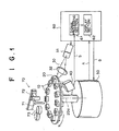
- a surface plasmon resonance sensor comprises a turn table 20 on which a plurality of measuring chips 10 in accordance with a first embodiment of the present invention are supported, a laser 31 such as a semiconductor laser which emits a measuring light beam 30, a condenser lens 32 which forms an incident optical system, a photodetector 40, a drive means 50 which intermittently rotates the turn table 20, a controller 60 which controls the drive means 50 and at the same time receives output signal S of the photodetector 40 to execute processing described later, and an automatic sample supply mechanism 70.
- a laser 31 such as a semiconductor laser which emits a measuring light beam 30
- a condenser lens 32 which forms an incident optical system
- a photodetector 40 which intermittently rotates the turn table 20
- a controller 60 which controls the drive means 50 and at the same time receives output signal S of the photodetector 40 to execute processing described later
- an automatic sample supply mechanism 70 an automatic sample supply mechanism
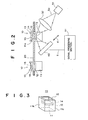
- each of the measuring chips 10 comprises a transparent dielectric block 11 which is rectangular in shape, a metal film 12 such as of gold, silver, cupper, aluminum or the like which is formed on the upper face of the block 11, and a sample holder frame (constituting a sample holder mechanism) 13 which is a tubular member defining above the metal film 12 a space having closed side walls.
- the dielectric block 11 is of a single piece which has all the face on which the metal film 12 is formed (a face forming an interface 11a to be described later), a light incident face 11 through which the measuring light beam 30 enters the block 11 and a light emanating face 11c through which the measuring light beam 30 emanates the block 11.
- the sample holder frame 13 is stored, for instance, a sample liquid 15 in the manner to be described later.
- the measuring chip 10 is formed, for instance, by integrally forming the dielectric block 11 and the sample holder frame 13 by injection molding of transparent resin and is replaceable.
- the measuring chips 10 are removably held in through holes formed in the turn table 20.
- a sensing medium 14 is fixed on the metal film 12. The sensing medium 14 will be described later.
- the transparent resin for forming the dielectric block 11 and the sample holder frame 13 PMMA, polycarbonate, amorphous polyolefin, cycloolefin and the like are preferred. Also glass may be preferably employed.
- the material for forming the dielectric block 11 those which are 1.45 to 2.5 or so in refractive index are generally preferred since a practical SPR angle is obtained in the refractive index range.
- the turn table 20 is arranged so that a plurality of (eleven in this particular embodiment) measuring chips 10 are supported on a circle about its axis of rotation 20a at regular intervals.
- the drive means 50 comprises a stepping motor and rotates the turn table 20 by an angle equal to the angular space between the chips 10.
- the condenser lens 32 condenses the light beam 30 and caused to enter the dielectric block 11 in the form of a convergent light beam so that various angles of incidence of the light beam 30 to the interface 11a of the dielectric block 11 and the metal film 12 can be obtained.
- the range of the angles of incidence is set to include a range in which the total internal reflection condition of the light beam 30 is satisfied at the interface 11a and a surface plasmon resonance can take place.
- the light beam 30 impinges upon the interface 11a in the form of p-polarized light.
- This can be realized by suitably positioning the laser 31 or by control the polarization direction of the light beam 30 by the use of a wavelength plate, a polarizing plate or the like.
- the photodetector 40 comprises a line sensor having a number of photodetector elements arranged in a row in the direction of arrow X in Figure 2 .
- the controller 60 receives an address signal A representing the position of the drive means 50 and outputs a drive signal D for driving the drive means 50 on the basis of a predetermined sequence. Further, the controller 60 is provided with a signal processing section 61 which receives an output signal S from the photodetector 40 and a display section 62 which receives an output of the signal processing section 61.
- the automatic sample supply mechanism 70 comprises a pipette 71 which sucks a predetermined amount of sample liquid and a pipette drive means 72 which moves the pipette 71.
- the automatic sample supply mechanism 70 causes the pipette 72 to suck the sample in a sample container 73 held in a predetermined position and moves the pipette 71 above the sample holder frame 13 of a measuring chip 10 in a predetermined position, and causes the pipette 71 to spot the sample liquid in the sample holder frame 13.
- the turn table 20 is intermittently rotated by the drive means 50.
- sample liquid 15 is supplied to the sample holder frame 13 of the measuring chip 10 in the predetermined position by the automatic sample supply mechanism 70.
- the laser 31 is driven under the control of the controller 60 and the light beam 30 emitted from the laser 31 impinges upon the interface 11a between the dielectric block 11 and the metal film 12 in the form of convergent light.
- the light beam 30 is reflected in total internal reflection at the interface 11a and is detected by the photodetector 40.
- the light beam 30 Since the light beam 30 impinges upon the interface 11a in the form of convergent light, the light beam 30 includes components which impinge upon the interface at various angles ⁇ .
- the angles ⁇ of incidence is not smaller than the angle of total internal reflection. Accordingly, the light beam 30 is reflected in total internal reflection at the interface 11a, and the reflected light beam 30 at the interface 11a includes components reflected at various reflecting angles.
- the optical system such as the condenser lens 32 may be arranged so that the light beam 30 impinges upon the interface 11 in a defocused state. This arrangement is advantageous in that errors in detecting the state of surface plasmon resonance, e.g., in detecting the position of the aforesaid dark line, are averaged, whereby the measuring accuracy is enhanced.
- FIG. 4 is a graph showing the relation between the angle of incidence ⁇ sp of the light beam 30 and the output (I) of the photodetector 40.
- the position of the photodetector element which detects the dark line can be determined and the angle ⁇ sp of incidence at which the intensity I of the light beam 30 reflected in total internal reflection at the interface 11a sharply drops can be determined. Accordingly by referring to a standard curve which represents the relation between the intensity I of the reflected light and the angle ⁇ sp of incidence at which the intensity I of the light beam 30 reflected in total internal reflection at the interface 11a sharply drops for each sample, a particular material in the sample 15 can be quantitatively analyzed.
- the signal processing section 61 of the controller 60 quantitatively analyzes the particular material in the sample 15 on the basis of this fact and the result of the analysis is displayed by the display section 62.
- the measuring chips 10 When each sample 15 is subjected to measurement only once, the measuring chips 10 may be manually or automatically removed from the turn table 20. Whereas when each sample 15 is subjected to measurement a plurality of times, the measuring chips 10 may be left on the turn table 20 so that the measuring chip 20 is brought to the measuring position again when the turn table 20 makes another rotation.
- the surface plasmon resonance sensor of this embodiment since a plurality of measuring chips 10 are held on the turn table 20 and the turn table 20 is intermittently rotated so that the measuring chips 10 are brought to the measuring position in sequence, a plurality of samples 15 can be measured at a high efficiency whereby the time required to measure each sample can be shortened.
- the automatic sample supply mechanism 70 since, the automatic sample supply mechanism 70 is provided, the time required to supply samples to the measuring chips 10 also can be shortened, whereby the time required to measure each sample can be further shortened.
- the measuring chip 10 of this embodiment need not be coupled with another dielectric block (as an optical coupler) by way of refractive index matching fluid, it is very easy to handle. Further, since it is not necessary to use the refractive index matching fluid, adverse influence of the fluid on the environment can be avoided.
- the sensing medium 14 fixed on the surface of the metal film 12 is selectively linked to a specific material in the sample 15.
- a specific material in the sample 15 for instance, combinations of antigen and antibody are known.
- antigen-antibody reaction can be detected on the basis of the angle ⁇ sp of total internal reflection attenuation.
- Figure 5 shows a measuring chip 10' in accordance with an example and a surface plasmon resonance sensor employing the measuring chip 10'.
- elements analogous to those shown in Figure 2 are given the same reference numerals and will not be described here.
- the measuring chip 10' of this example differs from the measuring chip 10 of the first embodiment in that the measuring chip 10' is not provided with the sensing medium 14. Accordingly, the specific material in the sample 15 is not linked with the sensing medium and the normal quantitative analysis of a material to be measured in the sample 15 is effected.
- the measuring chip 10' of the example is the same as the measuring chip 10 of the first embodiment.
- the measuring chip of the present invention is employed in an apparatus where a plurality of the measuring chips are mounted on the turn table 20 and automatically brought to and removed from the measuring position by rotating the turn table 20, the measuring chip of the present invention can be employed in a measuring apparatus where such an automatic measuring chip supply mechanism is not provided.
- the surface plasmon resonance sensor shown in Figure 6 comprises an attachment 80 which is fixed with respect to the laser 31, the condenser lens 32 and the photodetector 40.
- the measuring chip 10 is manually set to the attachment 80, and after measurement, the measuring chip 10 is manually replaced by new one.
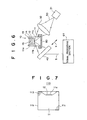
- the measuring chip 110 of the second embodiment of the present invention shown in Figure 7 is the same as the measuring chip 10, and in the measuring chip 110, the space inside the sample holder frame 113 is also flared upward. Since the metal film 12 is generally formed by deposition, when the sample holder mechanism 113 is of such a shape, the metal film 12 can be formed in a uniform thickness without being adversely affected by the sample holder frame 113.
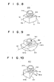
- the measuring chip 210 of the example shown in Figure 8 differs from that of the example shown in Figure 3 in that the sample holder frame 213 is cylindrical and the metal film 212 is circular.
- the sample holder frame 313 has a cylindrical inner space though is rectangular in outer shape.
- the metal film 312 is circular.
- the dielectric block 311 has a spherical light incident face 311b and a spherical light emanating face 311c.
- the light incident face 311b and the light emanating face 311c of the dielectric block 311 function like a lens to the light beam 30.
- the measuring chip 410 of the example shown in Figure 10 differs from that 210 of the example shown in Figure 8 in the shape of the dielectric block 411. That is, a part of the dielectric block 411 outside the optical path of the light beam 30 is cut away. With this arrangement, the material for forming the dielectric block can be saved.
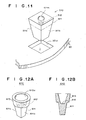
- the measuring chip 510 of the third embodiment and a surface plasmon resonance sensor in which the measuring chip 510 of the third embodiment is employed will be described with reference to Figure 11 , hereinbelow.
- the measuring chip 510 comprises a dielectric block 511 formed of transparent resin.
- the dielectric block 511 is of a quadrangular pyramid in outer shape which flares upward and is positioned with the smaller side down when it is set on the surface plasmon resonance sensor.
- two side faces form a light incident face 511b and a light emanating face 511c.
- the light incident face 511b and the light emanating face 511c of the dielectric body 511 may be transparent over the entire area or may be transparent only the part through which the light beam 30 travels.
- the other two faces may be transparent over the entire area or may be transparent only the part through which the light beam 30 travels, or may be semitransparent.
- a sample holder hole 511m which is tapered downward is formed on the top of the dielectric block 511 and a metal film 512 is formed on the bottom of the sample holder hole 511m. That is, in this embodiment, the part of the dielectric block 511 around the sample holder hole 511m forms the sample holder frame.
- the turn table 20 ( Figure 1 ) of the surface plasmon resonance sensor has a plurality of chip holding holes 20w which is of a quadrilateral in shape. Each of the chip holding holes 20w is tapered downward to conform to the outer shape of the dielectric block 511.
- the measuring chip 510 is inserted into the chip holding hole 20w from above and is held on the turn table 20 by way of engagement between the outer surface of the dielectric block 511 and inner surface of the chip holding hole 20w. Since the measuring chip 20w is positioned and held by way of engagement between the outer surface of the dielectric block 511 and the inner surface of the chip holding hole 20w which are both of quadrilateral in shape, the dielectric block 511 can be automatically oriented with respect to the turn table in the horizontal direction and cannot be moved from the position in the horizontal direction. With this arrangement, positioning of the measuring chip 510 in the horizontal direction is facilitated.
- the measuring chip can be automatically located also in the vertical direction.
- the part of the dielectric block 511 lower than the chained line in Figure 11 projects downward beyond the lower edge of the turn table 20.
- the measuring chip 610 of the fourth embodiment shown in Figures 12A and 12B differs from that 510 of the third embodiment in that a conical sample holding frame 613 provided with a conical sample holding hole 613a tapered downward is formed on the dielectric block 611 integrally therewith.
- a metal film 612 is formed on the bottom of the sample holding hole 613a.
- the dielectric block 611 of the measuring chip 601 of this embodiment is basically the same in the outer shape as the dielectric block 510 of the third embodiment. Out of the four side faces of the dielectric block 611, two side faces form a light incident face 611b and a light emanating face 611c. Since the dielectric block 611 is basically the same as that of the third embodiment in the outer shape, also the measuring chip 610 of this embodiment can be easily positioned in both the horizontal and vertical directions.
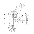
- FIG 13 is a side cross-sectional view partly cut away showing a measuring chip 700 in accordance with a further example and a leaky mode sensor employing the measuring chip 700.
- the leaky mode sensor is basically of the same structure as the surface plasmon resonance sensor shown in Figure 2 .
- the measuring chip 700 comprises a dielectric block 11, a clad layer 701 formed on the top surface of the dielectric block 11 and an optical waveguide layer 702 formed on the clad layer 701.
- the dielectric block 11 is formed of, for instance, synthetic resin or optical glass such as BK7.
- the clad layer 701 is formed of dielectric material lower than the dielectric block 11 in refractive index or metal such as gold.
- the optical wave guide layer 702 is formed of dielectric material such as PMMA which is higher than the clad layer 701 in refractive index.
- the thickness of the clad layer 701 is 36.5nm when it is formed gold film, and the thickness of the optical waveguide layer 702 is about 700nm when it is formed of PMMA.
- the leaky mode sensor when the light beam 30 emitted from the laser 31 is caused to impinge upon the clad layer 701 at an angle not smaller than an angle of total internal reflection, the light beam 30 is reflected in total internal reflection at the interface 11a of the dielectric block 11 and the clad layer 701, and only light having a particular wave number and impinging upon the waveguide layer 702 at a particular angle of incidence comes to propagate through the optical waveguide layer 702 in a waveguide mode after passing through the clad layer 701.
- the waveguide mode is thus excited, almost all the incident light is taken in the optical waveguide layer 702 and accordingly, the intensity of light reflected in total internal reflection at the interface 11a of the dielectric block 11 and the clad layer 701 sharply drops. That is, attenuation in total internal reflection occurs.
- the wave number of light to be propagated through the optical waveguide layer 702 in a waveguide mode depends upon the refractive index of the sample 15 on the optical waveguide layer 702, the refractive index and/or the properties of the sample 15 related to the refractive index can be detected on the basis of the angle of incidence at which the attenuation in total internal reflection occurs.
- a signal processing section 61 quantitatively analyzes the particular material in the sample 15 on the basis of this fact and the result of the analysis is displayed by the display section (not shown).
- the measuring chip 700 of this example need not be coupled with another dielectric block by way of refractive index matching fluid, it is very easy to handle. Further, since it is not necessary to use the refractive index matching fluid, adverse influence of the fluid on the environment can be avoided.
- a measuring chip 810 in accordance with the fifth embodiment of the present invention will be described with reference to Figures 14, 15A and 15B , hereinbelow.
- the measuring chip 810 of this embodiment is substantially the same as the measuring chip 510 of the third embodiment shown in Figure 11 except the shape of the sample holder hole 811m. That is, the measuring chip 810 comprises a dielectric block 811 formed of transparent resin.
- the dielectric block 811 is of a quadrangular pyramid in outer shape which flares upward and is positioned with the smaller side down when it is set on the surface plasmon resonance sensor.
- two side faces form a light incident face 811b and a light emanating face 811c.
- the light incident face 811b and the light emanating face 811c of the dielectric body 811 may be transparent over the entire area or may be transparent only the part through which the light beam 30 travels.
- the other two faces may be transparent over the entire area or may be transparent only the part through which the light beam 30 travels, or may be semitransparent.
- a sample holder hole 811m which is tapered downward is formed on the top of the dielectric block 811 and a metal film 812 is formed on the bottom of the sample holder hole 811m. That is, in this embodiment, the part of the dielectric block 811 around the sample holder hole 811m forms the sample holder frame.
- plastic injection molding When the dielectric block 811 is formed of transparent resin, plastic injection molding is generally employed. In plastic injection molding, when the product cannot be smoothly ejected from the injection mold, the product becomes of an irregular shape and a defective product is generated.
- the dielectric block 511 shown in Figure 11 can be relatively smoothly ejected from the injection mold since the sample holder hole 511m is tapered. However, a sharp edge defined between the side wall of the sample holder hole 511m and the bottom of the same can adversely affect ejection of the product.
- the sample holder hole 811m is formed like a bowl and the side wall of the sample holder hole 811m smoothly merges into the bottom of the same, the product can be ejected so smoothly from the injection mold that generation of defective products is suppressed to produce high yield.
- the metal film 812 can be formed in a uniform thickness without being adversely affected by the part around the sample holder hole 811m.
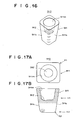
- a measuring chip 910 in accordance with the sixth embodiment of the present invention will be described with reference to Figures 16, 17A and 17B , hereinbelow.
- the measuring chip 910 of this embodiment is substantially the same as the measuring chip 810 of the fifth embodiment shown in Figures 14, 15A and 15B except the shape of the sample holder hole 911m and the outer shape of the dielectric block 911. That is, the measuring chip 910 comprises a dielectric block 911 formed of transparent resin.
- the dielectric block 911 is of a quadrangular pyramid in outer shape which flares upward and is positioned with the smaller side down when it is set on-the surface plasmon resonance sensor. Out of the four side faces of the dielectric block 911, two side faces form a light incident face 911b and a light emanating face 911c.
- the edges between adjacent side faces of the dielectric block 911 are rounded as indicated by arrow R1 in Figure 17A
- the corners between the side faces and the bottom face of the dielectric block 911 are rounded as indicated by arrow R2 in Figure 17B . That is, in both the horizontal cross-sections denoted by arrows v1 and v2, the corners of the dielectric block 911 are rounder.
- the rounded edges and the rounded corners permit the product to be smoothly ejected from the injection mold and suppress generation of defective products, whereby high yield is obtained.
- the shapes of the dielectric blocks 811 and 911 of the measuring chips in accordance with the fifth and sixth embodiments of the present invention may be also applied to the leaky mode sensor shown in Figure 13 and provide substantially the same results.
- the measuring system was basically the same as the surface plasmon resonance sensor shown in Figure 1 .
- Measuring chips 910 of the sixth embodiment were set in the chip holding holes 20w of the turn table 20 and the turn table 20 was rotated to bring the measuring chips 910 to the measuring position in sequence.
- the same light source and photodetector as shown in Figure 2 were used.
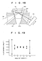
- Measuring chips 910 which were 1°, 3° , 7° , 10° , 15° and 20° in angle of taper ( ⁇ ), the angle between the vertical axis of the dielectric block 911 and the side faces of the same, were prepared, and at the same time, a measuring chip which was 0° in angle of taper ⁇ (not tapered) was prepared. Then the measuring chips were set on respective turn tables which were the same as the angles of taper ⁇ in angle of inclination of the chip holding holes 20w.
- Sensing medium 14 was fixed on the metal film 912 of each measuring chip and samples containing therein a specific material to be linked with the sensing medium 14.
- the specific material in the sample 15 is linked with the sensing medium 14, the refractive index of the sensing medium 14 is changed and the angle ⁇ sp at which attenuation in total internal reflection occurs changes.
- the change of the angle ⁇ sp at which attenuation in total internal reflection occurs is normally within 0.1 to 1.0°.
- fluctuation in the measured value of the angle ⁇ sp at which attenuation in total internal reflection occurs due to fluctuation in position of the measuring chip 910 should not exceed 1/10 of the range over which the angle ⁇ sp changes due to link of the specific material in the sample 15 with the sensing medium 14. That is, fluctuation in the measured value of the angle ⁇ sp due to fluctuation in position of the measuring chip should be not larger than 0.01° .
- the measuring chip is positioned with respect to the chip holder hole 20w of the turn table 20 by virtue of the tapered outer shape of the dielectric block, the measuring chip can be slightly displaced in the vertical direction as the turn table 20 is turned.
- the displacement of the measuring chip results in fluctuation in measured values of the angle ⁇ sp.
- the turn tables 20 which were loaded with the measuring chip having different angles of taper ⁇ were turned by one rotation and the difference between the measured values of the angle ⁇ sp before and after the rotation.
- the result is as shown in Figure 19 .
- fluctuation in the measured value of the angle ⁇ sp due to fluctuation in position of the measuring chip can be not larger than 0.01° when the angle of taper ⁇ is in the range 3 to 15°.
Landscapes
- Physics & Mathematics (AREA)
- Health & Medical Sciences (AREA)
- Life Sciences & Earth Sciences (AREA)
- Chemical & Material Sciences (AREA)
- Analytical Chemistry (AREA)
- Biochemistry (AREA)
- General Health & Medical Sciences (AREA)
- General Physics & Mathematics (AREA)
- Immunology (AREA)
- Pathology (AREA)
- Optical Measuring Cells (AREA)
- Investigating Or Analysing Materials By Optical Means (AREA)
- Automatic Analysis And Handling Materials Therefor (AREA)
Description
- This invention relates to a measuring apparatus according to the preamble of
claim 1, for instance, a surface plasmon resonance sensor for quantitatively analyzing a material in a sample utilizing generation of surface plasmon. - In metal, free electrons vibrate in a group to generate compression waves called plasma waves. The compression waves generated in a metal surface are quantized into surface plasmon.
- There have been proposed various surface plasmon resonance sensors for quantitatively analyzing a material in a sample utilizing a phenomenon that such surface plasmon is excited by light waves. Among those, one employing a system called "Kretschmann configuration" is best known. See, for instance, Japanese Unexamined Patent Publication No.
6(1994)-167443 - The plasmon resonance sensor using the Kretschmann configuration basically comprises a dielectric block shaped, for instance, like a prism, a metal film which is formed on one face of the dielectric block and is brought into contact with a sample, a light source emitting a light beam, an optical system which causes the light beam to enter the dielectric block so that the light beam is reflected in total internal reflection at the interface of the dielectric block and the metal film and various angles of incidence of the light beam to the interface of the dielectric block and the metal film including an angle of incidence at which surface plasmon is generated can be obtained, and a photodetector means which is able to detect the intensity of the light beam reflected in total internal reflection at the interface and detect a state of surface plasmon resonance.
- In order to obtain various angles of incidence of the light beam to the interface, a relatively thin incident light beam may be caused to impinge upon the interface while deflecting the incident light beam or a relatively thick incident light beam may be caused to impinge on the interface in the form of convergent light or divergent light so that components of the incident light beam impinge upon the interface at various angles. In the former case, the light beam which is reflected from the interface at an angle which varies as the incident light beam is deflected may be detected by a photodetector which is moved in synchronization with deflection of the incident light beam or by an area sensor extending in the direction in which reflected light beam is moved as a result of deflection. In the latter case, an area sensor which extends in directions so that all the components of light reflected from the interface at various angles can be detected by the area sensor may be used.
- In such a plasmon resonance sensor, when a light beam impinges upon the interface at a particular angle of incidence θsp not smaller than the angle of total internal reflection, evanescent waves having an electric field distribution in the sample in contact with the metal film are generated and surface plasmon is excited in the interface between the metal film and the sample. When the wave vector of the evanescent waves is equal to the wave number of the surface plasmon and wave number matching is established, the evanescent waves and the surface plasmon resonate and light energy is transferred to the surface plasmon, whereby the intensity of light reflected in total internal reflection at the interface of the dielectric block and the metal film sharply drops. The sharp intensity drop is generally detected as a dark line by the photodetector.
- The aforesaid resonance occurs only when the incident light beam is p-polarized. Accordingly, it is necessary to set the light beam to impinge upon the interface in the form of p-polarized light.
- When the wave number of the surface plasmon can be known from the angle of incidence θsp at which the phenomenon of attenuation in total internal reflection (ATR) takes place, the dielectric constant of the sample can be obtained. That is,

wherein Ksp represents the wave number of the surface plasmon, ω represents the angular frequency of the surface plasmon, c represents the speed of light in a vacuum, and ε m and ε s respectively represent the dielectric constants of the metal and the sample. - When the dielectric constant ε s of the sample is known, the concentration of a specific material in the sample can be determined on the basis of a predetermined calibration curve or the like. Accordingly, a specific component in the sample can be quantitatively analyzed by detecting the angle of incidence θsp at which the intensity of light reflected in total internal reflection from the interface of the prism and the metal film sharply drops.
- In the conventional plasmon resonance sensor of the type described above employing the system described above, it is practically necessary to change sample by sample the metal film to be brought into contact with the sample. Conventionally, the metal film is fixedly formed on a flat and thin dielectric plate as a unit and the unit is removably integrated with a prism-like dielectric block which functions as an optical coupler for causing total internal reflection. The prism-like dielectric block is fixedly provided with respect to the optical system and the unit of the metal film and the dielectric plate is changed sample by sample as a measuring chip.
- As a similar apparatus utilizing the phenomenon of attenuation in total internal reflection (ATR), there has been known a leaky mode sensor described in, for instance, T. Okamoto, "Spectrum Researches" Vol. 47, No.1 (1998), pp21 to 23 & pp26 and 27. The leaky mode sensor basically comprises a dielectric block shaped, for instance, like a prism, a clad layer which is formed on one face of the dielectric block, an optical waveguide layer which is formed on the clad layer and is brought into contact with a sample, a light source emitting a light beam, an optical system which causes the light beam to enter the dielectric block at various angles of incidence so that total internal reflection conditions are satisfied at the interface of the dielectric block and the clad layer, and a photodetector means which is able to detect the intensity of the light beam reflected in total internal reflection at the interface and detect an excited state of waveguide mode, i.e., attenuation in total internal reflection (ATR).
- In the leaky mode sensor with this arrangement, when the light beam is caused to impinge upon the clad layer through the dielectric block at an angle not smaller than an angle of total internal reflection, only light having a particular wave number and impinging upon the optical waveguide layer at a particular angle of incidence comes to propagate through the optical waveguide layer in a waveguide mode after passing through the clad layer. When the waveguide mode is thus excited, almost all the incident light is taken in the optical waveguide layer and accordingly, the intensity of light reflected in total internal reflection at the interface of the dielectric block and the clad layer sharply drops. That is, attenuation in total internal reflection occurs. Since the wave number of light to be propagated through the optical waveguide layer in a waveguide mode depends upon the refractive index of the sample on the optical waveguide layer, the refractive index and/or the properties of the sample related to the refractive index can be detected on the basis of the angle of incidence at which the attenuation in total internal reflection occurs.
- Also in the leaky mode sensor, it is possible to fix a dielectric block with respect to the optical system, to form the clad layer and the optical waveguide layer on another dielectric block to form a measuring chip, and to change the measuring chip sample by sample.
- However, when the conventional measuring chips are used, the dielectric blocks have to be integrated with each other by way of refractive index matching fluid in order to prevent a space from being formed between the dielectric blocks to make discontinuous the refractive index between the blocks. Such operation is very troublesome, which makes the conventional measuring chips inconvenient to handle. Especially, in an automated measuring system in which a plurality of measuring chips are loaded on a turret and the turret is rotated to bring the measuring chips in sequence to a measuring position where a light beam is projected onto each measuring chip, loading and unloading the measuring chips take a lot of labor, which is apt to cause deterioration in the measuring efficiency.
- Further, the refractive index matching fluid can adversely affect the environment.
- A measuring apparatus according to the preamble of
claim 1 is known fromEP 0 884 581 A1 . The sample is constituted by a liquid which is conveyed through a flow cell. AlsoWO 95/22754 claim 1. In this prior art apparatus, the space above the film layer is defined by walls which are perpendicularly oriented with respect to the film layer. -
WO 97/15819 -
JP 9 257 701 figures 7 and8 ) discloses a surface plasmon resonance sensor comprising a detecting piece which includes a prism part having a light reflection side formed by a vapour-deposited silver thin film. - In view of the foregoing observations and description, the object of the present invention is to provide a measuring apparatus which is easily replaceable and can eliminate necessity of using refractive index matching fluid.
- In accordance with the present invention, there is provided a measuring chip which is used in a measuring apparatus comprising the features of
claim 1. - The measuring apparatus is provided with a sample holder mechanism for holding the sample on the film layer. Specifically, the sample holder mechanism comprises a member which defines above the film layer a space having closed side walls and is flared upward. It is preferred that the inner surface of the member which defines above the film layer a space having closed side walls is smoothly merged with the first face of the dielectric block on which the film layer is formed.
- Further it is preferred that the dielectric block be polygonal such as a rectangle in a horizontal cross-section. In this specification, "the horizontal cross-section" means a cross-section taken along a plane perpendicular to the vertical direction of the block in which the block is positioned in operation of the measuring chip.
- When the dielectric block is polygonal in a horizontal cross-section, it is preferred that corners of the polygonal be rounded in at least one horizontal plane. The polygonal may be rounded at corners between two adjacent side surfaces thereof, at corners between two adjacent side surfaces and the bottom surface, and at both the corners.
- Further, when the dielectric block is polygonal in a horizontal cross-section, it is preferred that the dielectric block is tapered downward so that the cross-sectional area becomes larger upward. In this case, it is preferred that the inclined side surfaces of the dielectric block be at 3 to 15° to the vertical axis of the dielectric block.
- Preferably the dielectric block is formed of, for instance, glass or transparent resin. When the dielectric block is formed of transparent resin, it is preferred that the sample holder mechanism be formed integrally with the dielectric block.
- Further, it is preferred that a sensing medium which makes bonding reaction with a particular material in the sample be fixed on the film layer.
- In the measuring apparatus in accordance with the present invention since the single dielectric block has all the light incident face, the light emanating face and the face on which the film layer is formed and functions as an optical coupler, the measuring apparatus need be coupled with or decoupled from another member and accordingly, can be easily and quickly replaced.
- That is, unlike the prior art, the measuring chip of the present invention need not be coupled with another dielectric block (as an optical coupler) by way of refractive index matching fluid, and accordingly it is very easy to handle.
- Further, since it is not necessary to use the refractive index matching fluid, adverse influence of the fluid on the environment can be avoided.
- Since the sample holder mechanism comprises a member which defines above the film layer a space which has closed side walls and is flared upward, the film layer can be uniform in thickness. That is, since the film layer is generally formed by deposition, when the sample holder mechanism is of such a shape, the film layer can be uniformly formed without being adversely affected by the sample holder mechanism.
- Further, when the inner surface of the member which defines above the film layer a space having closed side walls is smoothly merged with the first face of the dielectric block on which the film layer is formed, plastic injection molding of the dielectric block/sample holder mechanism unit is facilitated since ejection of the products from the injection mold becomes smoother, whereby defective products can be reduced.
- When the dielectric block is polygonal in a horizontal cross-section and the corners of the polygonal are rounded in at least one horizontal plane, plastic injection molding of the dielectric block/sample holder mechanism unit is facilitated since ejection of the products from the injection mold becomes smoother, whereby defective products can be reduced.
- Further, when the dielectric block is polygonal in a horizontal cross-section and is tapered downward so that the cross-sectional area becomes larger upward, positioning of the measuring chip on the measuring apparatus is facilitated.
- That is, by forming a plurality of polygonal holes in a horizontal table of the measuring apparatus and holding the measuring chips by inserting the chips into the holes, the dielectric block can be automatically set in a predetermined direction in a horizontal plane and held there through engagement of polygons.
- By the same arrangement, the measuring chips can be automatically positioned also in the vertical direction.
- These inventors have found that when the inclined side surfaces of the dielectric block is at 3 to 15° to the vertical axis of the dielectric block, the measuring chip can be especially accurately positioned, the reason for which will become apparent later.
-
-
Figure 1 is a plan view of a surface plasmon resonance sensor employing a measuring apparatus including a chip in accordance with a first embodiment of the present invention, -
Figure 2 is a fragmentary side view showing a part of the surface plasmon resonance sensor, -
Figure 3 is a perspective view showing the measuring chip of an example not covered by the scope of the claims, -
Figure 4 is a graph showing the relation between the angle of incidence of a light beam and the output of the photodetector, -
Figure 5 is a side view partly cut away of a surface plasmon resonance sensor employing a measuring chip in accordance with a further example not covered by the scope of the claims, -
Figure 6 is a side view partly cut away of another example of a surface plasmon resonance sensor, -
Figure 7 is a side cross-sectional view of a measuring chip in accordance with a second embodiment of the present invention, -
Figure 8 is a perspective view of a measuring chip in accordance with a further example not covered by the scope of the claims, -
Figure 9 is a perspective view of a measuring chip in accordance with a further example not covered by the scope of the claims, -
Figure 10 is a perspective view of a measuring chip in accordance with a further example not covered by the scope of the claims, -
Figure 11 is a perspective view of a measuring chip in accordance with a third embodiment of the present invention, -
Figure 12A is a perspective view of a measuring chip in accordance with a fourth embodiment of the present invention, -
Figure 12B is a side cross-sectional view of a measuring chip in accordance with the fourth embodiment of the present invention, -
Figure 13 is a side cross-sectional view partly cut away showing a measuring chip in accordance with a further example not covered by the scope of the claims, and a leaky mode sensor employing the measuring chip, -
Figure 14 is a perspective view of a measuring chip in accordance with a fifth embodiment of the present invention, -
Figure 15A is a plan view of the measuring chip in accordance with the fifth embodiment of the present invention. -
Figure 15B a side cross-sectional view of the measuring chip in accordance with the fifth embodiment of the present invention, -
Figure 16 is a perspective view of a measuring chip in accordance with a sixth embodiment of the present invention, -
Figure 17A is a plan view of the measuring chip in accordance with the sixth embodiment of the present invention, -
Figure 17B a side cross-sectional view of the measuring chip in accordance with the sixth embodiment of the present invention, -
Figure 18 is a side view partly cut away of an apparatus for investigating a desirable angle of taper of the dielectric block, and -
Figure 19 is a graph showing the result of investigation. - In
Figures 1 to 3 , a surface plasmon resonance sensor comprises a turn table 20 on which a plurality of measuringchips 10 in accordance with a first embodiment of the present invention are supported, alaser 31 such as a semiconductor laser which emits a measuringlight beam 30, acondenser lens 32 which forms an incident optical system, aphotodetector 40, a drive means 50 which intermittently rotates the turn table 20, acontroller 60 which controls the drive means 50 and at the same time receives output signal S of thephotodetector 40 to execute processing described later, and an automaticsample supply mechanism 70. - As shown in
Figures 2 and 3 , each of the measuringchips 10 comprises atransparent dielectric block 11 which is rectangular in shape, ametal film 12 such as of gold, silver, cupper, aluminum or the like which is formed on the upper face of theblock 11, and a sample holder frame (constituting a sample holder mechanism) 13 which is a tubular member defining above the metal film 12 a space having closed side walls. Thedielectric block 11 is of a single piece which has all the face on which themetal film 12 is formed (a face forming aninterface 11a to be described later), alight incident face 11 through which the measuringlight beam 30 enters theblock 11 and alight emanating face 11c through which the measuringlight beam 30 emanates theblock 11. In thesample holder frame 13 is stored, for instance, asample liquid 15 in the manner to be described later. - The measuring
chip 10 is formed, for instance, by integrally forming thedielectric block 11 and thesample holder frame 13 by injection molding of transparent resin and is replaceable. In this particular embodiment, the measuringchips 10 are removably held in through holes formed in the turn table 20. Further, in this particular embodiment, asensing medium 14 is fixed on themetal film 12. Thesensing medium 14 will be described later. - As the transparent resin for forming the
dielectric block 11 and thesample holder frame 13, PMMA, polycarbonate, amorphous polyolefin, cycloolefin and the like are preferred. Also glass may be preferably employed. As the material for forming thedielectric block 11, those which are 1.45 to 2.5 or so in refractive index are generally preferred since a practical SPR angle is obtained in the refractive index range. - The turn table 20 is arranged so that a plurality of (eleven in this particular embodiment) measuring
chips 10 are supported on a circle about its axis of rotation 20a at regular intervals. The drive means 50 comprises a stepping motor and rotates the turn table 20 by an angle equal to the angular space between thechips 10. - As shown in
Figure 2 , thecondenser lens 32 condenses thelight beam 30 and caused to enter thedielectric block 11 in the form of a convergent light beam so that various angles of incidence of thelight beam 30 to theinterface 11a of thedielectric block 11 and themetal film 12 can be obtained. The range of the angles of incidence is set to include a range in which the total internal reflection condition of thelight beam 30 is satisfied at theinterface 11a and a surface plasmon resonance can take place. - The
light beam 30 impinges upon theinterface 11a in the form of p-polarized light. This can be realized by suitably positioning thelaser 31 or by control the polarization direction of thelight beam 30 by the use of a wavelength plate, a polarizing plate or the like. - The
photodetector 40 comprises a line sensor having a number of photodetector elements arranged in a row in the direction of arrow X inFigure 2 . - The
controller 60 receives an address signal A representing the position of the drive means 50 and outputs a drive signal D for driving the drive means 50 on the basis of a predetermined sequence. Further, thecontroller 60 is provided with asignal processing section 61 which receives an output signal S from thephotodetector 40 and adisplay section 62 which receives an output of thesignal processing section 61. - The automatic
sample supply mechanism 70 comprises apipette 71 which sucks a predetermined amount of sample liquid and a pipette drive means 72 which moves thepipette 71. The automaticsample supply mechanism 70 causes thepipette 72 to suck the sample in asample container 73 held in a predetermined position and moves thepipette 71 above thesample holder frame 13 of ameasuring chip 10 in a predetermined position, and causes thepipette 71 to spot the sample liquid in thesample holder frame 13. - Operation of the surface plasmon resonance sensor will be described hereinbelow. The turn table 20 is intermittently rotated by the drive means 50. When the turn table 20 is stopped,
sample liquid 15 is supplied to thesample holder frame 13 of themeasuring chip 10 in the predetermined position by the automaticsample supply mechanism 70. - When a
measuring chip 10 thesample holder frame 13 of which contains therein thesample liquid 15 is stopped in a predetermined measuring position (the position of the rightside measuring chip 10 inFigure 2 ), thelaser 31 is driven under the control of thecontroller 60 and thelight beam 30 emitted from thelaser 31 impinges upon theinterface 11a between thedielectric block 11 and themetal film 12 in the form of convergent light. Thelight beam 30 is reflected in total internal reflection at theinterface 11a and is detected by thephotodetector 40. - Since the
light beam 30 impinges upon theinterface 11a in the form of convergent light, thelight beam 30 includes components which impinge upon the interface at various angles θ. The angles θ of incidence is not smaller than the angle of total internal reflection. Accordingly, thelight beam 30 is reflected in total internal reflection at theinterface 11a, and the reflectedlight beam 30 at theinterface 11a includes components reflected at various reflecting angles. The optical system such as thecondenser lens 32 may be arranged so that thelight beam 30 impinges upon theinterface 11 in a defocused state. This arrangement is advantageous in that errors in detecting the state of surface plasmon resonance, e.g., in detecting the position of the aforesaid dark line, are averaged, whereby the measuring accuracy is enhanced. - When the
light beam 30 is reflected in total internal reflection at theinterface 11a, evanescent waves ooze out from theinterface 11a toward themetal film 12 and excite surface plasmon on the surface of themetal film 12. The component of thelight beam 30 which impinges upon the interface at a specified angle θ sp resonate with the surface plasmon excited on the surface of themetal film 12 and accordingly, the intensity I of the component of thelight beam 30 reflected in total internal reflection at theinterface 11a sharply drops.Figure 4 is a graph showing the relation between the angle of incidence θ sp of thelight beam 30 and the output (I) of thephotodetector 40. - By detecting the amount of reflected light received by each photodetector element on the basis of the output signal of the
photodetector 40, the position of the photodetector element which detects the dark line can be determined and the angle θ sp of incidence at which the intensity I of thelight beam 30 reflected in total internal reflection at theinterface 11a sharply drops can be determined. Accordingly by referring to a standard curve which represents the relation between the intensity I of the reflected light and the angle θ sp of incidence at which the intensity I of thelight beam 30 reflected in total internal reflection at theinterface 11a sharply drops for each sample, a particular material in thesample 15 can be quantitatively analyzed. Thesignal processing section 61 of thecontroller 60 quantitatively analyzes the particular material in thesample 15 on the basis of this fact and the result of the analysis is displayed by thedisplay section 62. - When each
sample 15 is subjected to measurement only once, the measuringchips 10 may be manually or automatically removed from the turn table 20. Whereas when eachsample 15 is subjected to measurement a plurality of times, the measuringchips 10 may be left on the turn table 20 so that the measuringchip 20 is brought to the measuring position again when the turn table 20 makes another rotation. - As described above, in the surface plasmon resonance sensor of this embodiment, since a plurality of measuring
chips 10 are held on the turn table 20 and the turn table 20 is intermittently rotated so that the measuringchips 10 are brought to the measuring position in sequence, a plurality ofsamples 15 can be measured at a high efficiency whereby the time required to measure each sample can be shortened. - Further, since, the automatic
sample supply mechanism 70 is provided, the time required to supply samples to the measuringchips 10 also can be shortened, whereby the time required to measure each sample can be further shortened. - Further, by replacing by a new measuring chip 10 a
measuring chip 10 holding thesample 15 which is already measured,new samples 15 can be measured immediately, whereby the time required to measure a plurality of samples can be further shortened. - Further since, unlike the prior art, the measuring
chip 10 of this embodiment need not be coupled with another dielectric block (as an optical coupler) by way of refractive index matching fluid, it is very easy to handle. Further, since it is not necessary to use the refractive index matching fluid, adverse influence of the fluid on the environment can be avoided. - The
sensing medium 14 fixed on the surface of themetal film 12 is selectively linked to a specific material in thesample 15. As such a combination of thesensing medium 14 and the specific material in thesample 15, for instance, combinations of antigen and antibody are known. In such a case, antigen-antibody reaction can be detected on the basis of the angle θ sp of total internal reflection attenuation. -
Figure 5 shows a measuring chip 10' in accordance with an example and a surface plasmon resonance sensor employing the measuring chip 10'. InFigure 5 , elements analogous to those shown inFigure 2 are given the same reference numerals and will not be described here. - The measuring chip 10' of this example differs from the measuring
chip 10 of the first embodiment in that the measuring chip 10' is not provided with thesensing medium 14. Accordingly, the specific material in thesample 15 is not linked with the sensing medium and the normal quantitative analysis of a material to be measured in thesample 15 is effected. - Except this point, the measuring chip 10' of the example is the same as the measuring
chip 10 of the first embodiment. - Though, the measuring chip of the present invention is employed in an apparatus where a plurality of the measuring chips are mounted on the turn table 20 and automatically brought to and removed from the measuring position by rotating the turn table 20, the measuring chip of the present invention can be employed in a measuring apparatus where such an automatic measuring chip supply mechanism is not provided. For example, the surface plasmon resonance sensor shown in
Figure 6 comprises anattachment 80 which is fixed with respect to thelaser 31, thecondenser lens 32 and thephotodetector 40. In the surface plasmon resonance sensor shown inFigure 6 , the measuringchip 10 is manually set to theattachment 80, and after measurement, the measuringchip 10 is manually replaced by new one. - Second to sixth embodiments of the present invention will be described with reference to
Figures 7 to 17B , hereinbelow. - The
measuring chip 110 of the second embodiment of the present invention shown inFigure 7 is the same as the measuringchip 10, and in themeasuring chip 110, the space inside thesample holder frame 113 is also flared upward. Since themetal film 12 is generally formed by deposition, when thesample holder mechanism 113 is of such a shape, themetal film 12 can be formed in a uniform thickness without being adversely affected by thesample holder frame 113. - The
measuring chip 210 of the example shown inFigure 8 differs from that of the example shown inFigure 3 in that thesample holder frame 213 is cylindrical and themetal film 212 is circular. - In the measuring chip of theexample shown in
Figure 9 , thesample holder frame 313 has a cylindrical inner space though is rectangular in outer shape. Themetal film 312 is circular. Further thedielectric block 311 has a spherical light incident face 311b and a sphericallight emanating face 311c. The light incident face 311b and thelight emanating face 311c of thedielectric block 311 function like a lens to thelight beam 30. - The
measuring chip 410 of the example shown inFigure 10 differs from that 210 of the example shown inFigure 8 in the shape of thedielectric block 411. That is, a part of thedielectric block 411 outside the optical path of thelight beam 30 is cut away. With this arrangement, the material for forming the dielectric block can be saved. - The
measuring chip 510 of the third embodiment and a surface plasmon resonance sensor in which themeasuring chip 510 of the third embodiment is employed will be described with reference toFigure 11 , hereinbelow. Themeasuring chip 510 comprises adielectric block 511 formed of transparent resin. Thedielectric block 511 is of a quadrangular pyramid in outer shape which flares upward and is positioned with the smaller side down when it is set on the surface plasmon resonance sensor. - Out of the four side faces of the
dielectric block 511, two side faces form a light incident face 511b and alight emanating face 511c. The light incident face 511b and thelight emanating face 511c of thedielectric body 511 may be transparent over the entire area or may be transparent only the part through which thelight beam 30 travels. The other two faces may be transparent over the entire area or may be transparent only the part through which thelight beam 30 travels, or may be semitransparent. - A
sample holder hole 511m which is tapered downward is formed on the top of thedielectric block 511 and ametal film 512 is formed on the bottom of thesample holder hole 511m. That is, in this embodiment, the part of thedielectric block 511 around thesample holder hole 511m forms the sample holder frame. - The turn table 20 (
Figure 1 ) of the surface plasmon resonance sensor has a plurality ofchip holding holes 20w which is of a quadrilateral in shape. Each of thechip holding holes 20w is tapered downward to conform to the outer shape of thedielectric block 511. - The
measuring chip 510 is inserted into thechip holding hole 20w from above and is held on the turn table 20 by way of engagement between the outer surface of thedielectric block 511 and inner surface of thechip holding hole 20w. Since themeasuring chip 20w is positioned and held by way of engagement between the outer surface of thedielectric block 511 and the inner surface of thechip holding hole 20w which are both of quadrilateral in shape, thedielectric block 511 can be automatically oriented with respect to the turn table in the horizontal direction and cannot be moved from the position in the horizontal direction. With this arrangement, positioning of themeasuring chip 510 in the horizontal direction is facilitated. - Further, since the outer surface of the
dielectric block 511 and the inner surface of thechip holding hole 20w are both tapered downward, the measuring chip can be automatically located also in the vertical direction. In themeasuring chip 510 of this embodiment, the part of thedielectric block 511 lower than the chained line inFigure 11 projects downward beyond the lower edge of the turn table 20. - The
measuring chip 610 of the fourth embodiment shown inFigures 12A and 12B differs from that 510 of the third embodiment in that a conicalsample holding frame 613 provided with a conicalsample holding hole 613a tapered downward is formed on thedielectric block 611 integrally therewith. Ametal film 612 is formed on the bottom of thesample holding hole 613a. - The
dielectric block 611 of the measuring chip 601 of this embodiment is basically the same in the outer shape as thedielectric block 510 of the third embodiment. Out of the four side faces of thedielectric block 611, two side faces form alight incident face 611b and alight emanating face 611c. Since thedielectric block 611 is basically the same as that of the third embodiment in the outer shape, also themeasuring chip 610 of this embodiment can be easily positioned in both the horizontal and vertical directions. -
Figure 13 is a side cross-sectional view partly cut away showing ameasuring chip 700 in accordance with a further example and a leaky mode sensor employing themeasuring chip 700. The leaky mode sensor is basically of the same structure as the surface plasmon resonance sensor shown inFigure 2 . Themeasuring chip 700 comprises adielectric block 11, aclad layer 701 formed on the top surface of thedielectric block 11 and anoptical waveguide layer 702 formed on theclad layer 701. - The
dielectric block 11 is formed of, for instance, synthetic resin or optical glass such as BK7. Theclad layer 701 is formed of dielectric material lower than thedielectric block 11 in refractive index or metal such as gold. The opticalwave guide layer 702 is formed of dielectric material such as PMMA which is higher than theclad layer 701 in refractive index. The thickness of theclad layer 701 is 36.5nm when it is formed gold film, and the thickness of theoptical waveguide layer 702 is about 700nm when it is formed of PMMA. - In the leaky mode sensor, when the
light beam 30 emitted from thelaser 31 is caused to impinge upon theclad layer 701 at an angle not smaller than an angle of total internal reflection, thelight beam 30 is reflected in total internal reflection at theinterface 11a of thedielectric block 11 and theclad layer 701, and only light having a particular wave number and impinging upon thewaveguide layer 702 at a particular angle of incidence comes to propagate through theoptical waveguide layer 702 in a waveguide mode after passing through theclad layer 701. When the waveguide mode is thus excited, almost all the incident light is taken in theoptical waveguide layer 702 and accordingly, the intensity of light reflected in total internal reflection at theinterface 11a of thedielectric block 11 and theclad layer 701 sharply drops. That is, attenuation in total internal reflection occurs. - Since the wave number of light to be propagated through the
optical waveguide layer 702 in a waveguide mode depends upon the refractive index of thesample 15 on theoptical waveguide layer 702, the refractive index and/or the properties of thesample 15 related to the refractive index can be detected on the basis of the angle of incidence at which the attenuation in total internal reflection occurs. Asignal processing section 61 quantitatively analyzes the particular material in thesample 15 on the basis of this fact and the result of the analysis is displayed by the display section (not shown). - As the
measuring chip 10 of the first embodiment, themeasuring chip 700 of this example need not be coupled with another dielectric block by way of refractive index matching fluid, it is very easy to handle. Further, since it is not necessary to use the refractive index matching fluid, adverse influence of the fluid on the environment can be avoided. - A
measuring chip 810 in accordance with the fifth embodiment of the present invention will be described with reference toFigures 14, 15A and 15B , hereinbelow. - The
measuring chip 810 of this embodiment is substantially the same as themeasuring chip 510 of the third embodiment shown inFigure 11 except the shape of thesample holder hole 811m. That is, themeasuring chip 810 comprises adielectric block 811 formed of transparent resin. Thedielectric block 811 is of a quadrangular pyramid in outer shape which flares upward and is positioned with the smaller side down when it is set on the surface plasmon resonance sensor. - Out of the four side faces of the
dielectric block 811, two side faces form alight incident face 811b and alight emanating face 811c. Thelight incident face 811b and thelight emanating face 811c of thedielectric body 811 may be transparent over the entire area or may be transparent only the part through which thelight beam 30 travels. The other two faces may be transparent over the entire area or may be transparent only the part through which thelight beam 30 travels, or may be semitransparent. - A
sample holder hole 811m which is tapered downward is formed on the top of thedielectric block 811 and ametal film 812 is formed on the bottom of thesample holder hole 811m. That is, in this embodiment, the part of thedielectric block 811 around thesample holder hole 811m forms the sample holder frame. - When the
dielectric block 811 is formed of transparent resin, plastic injection molding is generally employed. In plastic injection molding, when the product cannot be smoothly ejected from the injection mold, the product becomes of an irregular shape and a defective product is generated. Thedielectric block 511 shown inFigure 11 can be relatively smoothly ejected from the injection mold since thesample holder hole 511m is tapered. However, a sharp edge defined between the side wall of thesample holder hole 511m and the bottom of the same can adversely affect ejection of the product. - To the contrast, in the
measuring chip 810 of the fifth embodiment, thesample holder hole 811m is formed like a bowl and the side wall of thesample holder hole 811m smoothly merges into the bottom of the same, the product can be ejected so smoothly from the injection mold that generation of defective products is suppressed to produce high yield. - As in the
measuring chip 110 shown inFigure 7 , since thesample holder hole 811m is flared upward, themetal film 812 can be formed in a uniform thickness without being adversely affected by the part around thesample holder hole 811m. - A
measuring chip 910 in accordance with the sixth embodiment of the present invention will be described with reference toFigures 16, 17A and 17B , hereinbelow. - The
measuring chip 910 of this embodiment is substantially the same as themeasuring chip 810 of the fifth embodiment shown inFigures 14, 15A and 15B except the shape of thesample holder hole 911m and the outer shape of thedielectric block 911. That is, themeasuring chip 910 comprises adielectric block 911 formed of transparent resin. - The
dielectric block 911 is of a quadrangular pyramid in outer shape which flares upward and is positioned with the smaller side down when it is set on-the surface plasmon resonance sensor. Out of the four side faces of thedielectric block 911, two side faces form alight incident face 911b and alight emanating face 911c. - The edges between adjacent side faces of the
dielectric block 911 are rounded as indicated by arrow R1 inFigure 17A , and the corners between the side faces and the bottom face of thedielectric block 911 are rounded as indicated by arrow R2 inFigure 17B . That is, in both the horizontal cross-sections denoted by arrows v1 and v2, the corners of thedielectric block 911 are rounder. - When the
dielectric block 911 is formed by plastic injection molding, the rounded edges and the rounded corners permit the product to be smoothly ejected from the injection mold and suppress generation of defective products, whereby high yield is obtained. - The shapes of the dielectric blocks 811 and 911 of the measuring chips in accordance with the fifth and sixth embodiments of the present invention may be also applied to the leaky mode sensor shown in
Figure 13 and provide substantially the same results. - The preferred angle of taper when the dielectric block is shaped in a polygonal in horizontal cross-section and is tapered downward as in the third, fourth, fifth and sixth embodiments will be discussed hereinbelow.
- We have investigated the range of the preferred angle of taper by the use of the measuring system shown in
Figure 18 . The measuring system was basically the same as the surface plasmon resonance sensor shown inFigure 1 . Measuringchips 910 of the sixth embodiment were set in thechip holding holes 20w of the turn table 20 and the turn table 20 was rotated to bring the measuringchips 910 to the measuring position in sequence. Though not shown, the same light source and photodetector as shown inFigure 2 were used. - Measuring
chips 910 which were 1°, 3° , 7° , 10° , 15° and 20° in angle of taper (δ), the angle between the vertical axis of thedielectric block 911 and the side faces of the same, were prepared, and at the same time, a measuring chip which was 0° in angle of taper δ (not tapered) was prepared. Then the measuring chips were set on respective turn tables which were the same as the angles of taper δ in angle of inclination of thechip holding holes 20w. Sensingmedium 14 was fixed on themetal film 912 of each measuring chip and samples containing therein a specific material to be linked with thesensing medium 14. - A component impinging upon the interface of the
dielectric block 911 and themetal film 912 at an angle θ sp at which attenuation in total internal reflection occurs greatly deteriorates in the intensity of reflected light and the deterioration is observed as a dark line in the reflected light. When the specific material in thesample 15 is linked with thesensing medium 14, the refractive index of thesensing medium 14 is changed and the angle θsp at which attenuation in total internal reflection occurs changes. The change of the angle θ sp at which attenuation in total internal reflection occurs is normally within 0.1 to 1.0°. In order to correctly detect the change of the angle θ sp at which attenuation in total internal reflection occurs, fluctuation in the measured value of the angle θ sp at which attenuation in total internal reflection occurs due to fluctuation in position of themeasuring chip 910 should not exceed 1/10 of the range over which the angle θ sp changes due to link of the specific material in thesample 15 with thesensing medium 14. That is, fluctuation in the measured value of the angle θ sp due to fluctuation in position of the measuring chip should be not larger than 0.01° . - Though the measuring chip is positioned with respect to the
chip holder hole 20w of the turn table 20 by virtue of the tapered outer shape of the dielectric block, the measuring chip can be slightly displaced in the vertical direction as the turn table 20 is turned. The displacement of the measuring chip results in fluctuation in measured values of the angle θ sp. After link of the specific material and the sensing material was stabilized, the turn tables 20 which were loaded with the measuring chip having different angles of taper δ were turned by one rotation and the difference between the measured values of the angle θ sp before and after the rotation. The result is as shown inFigure 19 . As can be understood fromFigure 19 , fluctuation in the measured value of the angle θ sp due to fluctuation in position of the measuring chip can be not larger than 0.01° when the angle of taper δ is in therange 3 to 15°.
Claims (10)
- A measuring apparatus including a chip (10; ...910) comprising:a dielectric block, (11; ...911)a film layer(12; ...912) which is formed on a first face of the dielectric block (11; ... 911) and is in contact with a sample(15), a light source (31) adapted to emit a light beam (30), an optical system (32) adapted to cause the light beam (30) to enter the dielectric block(11; ...911) through a second face (11 c) thereof so that the light beam (30) is reflected in total internal reflection at the interface (11 a) of the dielectric block (11; ...911) and the film layer(12; ...912) and various angles of incidence of the light beam (30) to the interface of the dielectric block (11; ...911) and the film layer (12) are obtained,and a photodetector means (40), adapted to detect attenuation in total internal reflection by detecting the intensity of the light beam (30), which is reflected in total internal reflection at the interface and goes outside the dielectric block (11) through a third face (11b) thereof, whereinthe measuring chip (10; ...910) comprises said dielectric block(11) having all the first to third faces (11 a, 11c, 11b), and the film layer(12; ...912) is integrally formed on the first face of the dielectric block (11), and whereina sample holder mechanism (13', 113) is provided for holding the sample on the film layer (12),the sample holder mechanism comprises a member (13) which defines above the film layer (12; ...912) a space which has closed side walls, characterized in that the space is flared upward.
- A measuring apparatus as defined in Claim 1 in which an inner surface of the member which defines above the film layer (12; ...912) the space having closed side walls is smoothly merged with the first face (11 a) of the dielectric block (11; ...911) on which the film layer (12; ...912) is formed.
- A measuring apparatus as defined in Claim 1 in which the dielectric block (511; 811) is polygonal in a horizontal cross-section.
- A measuring apparatus as defined in Claim 3 in which the corners of the polygonal are rounded when viewed in a horizontal cross-section.
- A measuring apparatus as defined in Claim 3 in which the dielectric block (511; ...911) is tapered downward so that the cross-sectional area becomes larger upward.
- A measuring apparatus as defined in Claim 5 in which the inclined side surfaces of the dielectric block are at 3 to 15° to a vertical axis of the dielectric block (511; ... 911).
- A measuring apparatus as defined in Claim 1 in which the dielectric block is formed of glass or transparent resin.
- A measuring apparatus as defined in Claim 1 in which a sensing medium which makes a bonding reaction with a particular material in the sample is fixed on the film layer(12; ...912).
- A Measuring apparatus as defined in any of claims 1 to 8 in the form of a surface plasmon resonance sensor, wherein said film layer is
a metal film layer, and wherein said photodetector means (40) is adapted to detect attenuation in total internal reflection due to plasmon resonance. - A measuring apparatus according to any of claims 1 to 8, in the form of a leaky mode sensor wherein
said film layer is composed of a clad layer which is formed on the first face of the dielectric block and an optical waveguide layer which is formed on the clad layer and is in contact with the sample,
wherein said photodetector means (40) is adapted to detect attenuation in total internal reflection due to excitation of a waveguide mode in the optical waveguide layer, and
the clad layer and the waveguide layer are integrally formed on the first face of the dielectric block.
Applications Claiming Priority (8)
| Application Number | Priority Date | Filing Date | Title |
|---|---|---|---|
| JP2000138604 | 2000-05-11 | ||
| JP2000138604 | 2000-05-11 | ||
| JP2000212125 | 2000-07-13 | ||
| JP2000212125 | 2000-07-13 | ||
| JP2001016633 | 2001-01-25 | ||
| JP2001016633 | 2001-01-25 | ||
| JP2001092666A JP4368535B2 (en) | 2000-05-11 | 2001-03-28 | Measuring chip |
| JP2001092666 | 2001-03-28 |
Publications (2)
| Publication Number | Publication Date |
|---|---|
| EP1154259A1 EP1154259A1 (en) | 2001-11-14 |
| EP1154259B1 true EP1154259B1 (en) | 2011-07-13 |
Family
ID=27481283
Family Applications (1)
| Application Number | Title | Priority Date | Filing Date |
|---|---|---|---|
| EP20010111432 Expired - Lifetime EP1154259B1 (en) | 2000-05-11 | 2001-05-10 | Measuring apparatus including a measuring chip |
Country Status (3)
| Country | Link |
|---|---|
| US (1) | US6597456B2 (en) |
| EP (1) | EP1154259B1 (en) |
| JP (1) | JP4368535B2 (en) |
Families Citing this family (28)
| Publication number | Priority date | Publication date | Assignee | Title |
|---|---|---|---|---|
| US20020127706A1 (en) * | 2001-01-25 | 2002-09-12 | Fuji Photo Film Co., Ltd. | Surface plasmon resonance measuring chip and method of manufacture thereof |
| US7767131B2 (en) * | 2001-08-30 | 2010-08-03 | Bayer Technology Services Gmbh | Method for production of moulded bodies, in particular optical structures and use thereof |
| JP2003106992A (en) * | 2001-09-28 | 2003-04-09 | Fuji Photo Optical Co Ltd | Measurement chip and its manufacturing method |
| JP2003139694A (en) * | 2001-11-06 | 2003-05-14 | Fuji Photo Film Co Ltd | Measurement plate |
| US7187444B2 (en) * | 2001-11-12 | 2007-03-06 | Fuji Photo Film Co., Ltd. | Measuring method and apparatus using attenuation in total internal reflection |
| JP4382339B2 (en) | 2001-12-14 | 2009-12-09 | 富士フイルム株式会社 | Measuring chip |
| EP1324019B1 (en) * | 2001-12-25 | 2006-07-12 | Fuji Photo Film Co., Ltd. | Sensor utilizing evanescent wave |
| JP3801914B2 (en) * | 2001-12-25 | 2006-07-26 | 富士写真フイルム株式会社 | How to reuse measurement tips |
| JP4173725B2 (en) * | 2001-12-25 | 2008-10-29 | 富士フイルム株式会社 | Sensors using evanescent waves |
| JP4030796B2 (en) * | 2002-05-13 | 2008-01-09 | 富士フイルム株式会社 | Measuring chip |
| JP3786073B2 (en) * | 2002-10-10 | 2006-06-14 | 株式会社日立製作所 | Biochemical sensor kit and measuring device |
| JP2005077317A (en) * | 2003-09-02 | 2005-03-24 | Fuji Photo Film Co Ltd | Measuring device |
| EP1512961B1 (en) * | 2003-09-02 | 2010-01-13 | FUJIFILM Corporation | Measuring apparatus based on surface plasmon resonance |
| JP2005257455A (en) * | 2004-03-11 | 2005-09-22 | Fuji Photo Film Co Ltd | Measuring apparatus and measuring unit |
| JP4455362B2 (en) * | 2004-03-11 | 2010-04-21 | 富士フイルム株式会社 | Measuring device using total reflection attenuation |
| US7187446B2 (en) * | 2004-07-26 | 2007-03-06 | Fuji Photo Film Co., Ltd. | Measuring apparatus |
| US20070243633A1 (en) * | 2004-09-30 | 2007-10-18 | Fuji Photo Film Co., Ltd. | Biosensor |
| JP4270511B2 (en) * | 2005-02-28 | 2009-06-03 | 富士フイルム株式会社 | Biosensor |
| JP4435709B2 (en) * | 2005-03-22 | 2010-03-24 | 富士フイルム株式会社 | Biosensor |
| JP4435708B2 (en) * | 2005-03-22 | 2010-03-24 | 富士フイルム株式会社 | Biosensor |
| JP2007248361A (en) * | 2006-03-17 | 2007-09-27 | Toshiba Corp | Antibody chip, antigen measuring device, and liquid ejection method |
| GB2441780B (en) * | 2006-08-07 | 2009-05-20 | Toshiba Res Europ Ltd | An apparatus for measuring a signal from a carrier with surface plasmon characteristics |
| US8804114B2 (en) | 2010-11-03 | 2014-08-12 | Pocared Diagnostics Ltd. | Optical cup |
| EP2698624A1 (en) * | 2012-08-16 | 2014-02-19 | Siemens Healthcare Diagnostics Products GmbH | Reaction container |
| CN104955957B (en) | 2012-12-11 | 2019-01-11 | 普凯尔德诊断技术有限公司 | optics cup with curved bottom |
| US10337994B2 (en) * | 2016-09-20 | 2019-07-02 | Kabushiki Kaisha Toshiba | Sample liquid measuring device and measuring method |
| CN109943476A (en) * | 2019-04-16 | 2019-06-28 | 北京龙基高科生物科技有限公司 | A kind of genetic chip sequencing equipment |
| CN115839930B (en) * | 2023-02-14 | 2023-05-12 | 成都华芯众合电子科技有限公司 | Optical platform for measuring refractive index of liquid through plasmon resonance |
Family Cites Families (9)
| Publication number | Priority date | Publication date | Assignee | Title |
|---|---|---|---|---|
| GB8813307D0 (en) * | 1988-06-06 | 1988-07-13 | Amersham Int Plc | Biological sensors |
| GB9019123D0 (en) * | 1990-09-01 | 1990-10-17 | Fisons Plc | Analytical device |
| JPH06167443A (en) | 1992-10-23 | 1994-06-14 | Olympus Optical Co Ltd | Measuring apparatus utilizing surface plasmon resonance |
| FI96800C (en) | 1994-02-16 | 1996-08-26 | Valtion Teknillinen | Device for performing an analysis |
| US5822073A (en) | 1995-10-25 | 1998-10-13 | University Of Washington | Optical lightpipe sensor based on surface plasmon resonance |
| JPH09257701A (en) | 1996-03-21 | 1997-10-03 | Toto Ltd | Surface plasmon resonance sensor |
| EP0884581A1 (en) | 1997-06-13 | 1998-12-16 | Hoechst Aktiengesellschaft | Optical sensor for detecting chemical substances dissolved or dispersed in water |
| JP3739537B2 (en) * | 1997-03-26 | 2006-01-25 | 大日本印刷株式会社 | Measuring chip for optical analyzer |
| GB9803704D0 (en) * | 1998-02-24 | 1998-04-15 | Univ Manchester | Waveguide structure |
-
2001
- 2001-03-28 JP JP2001092666A patent/JP4368535B2/en not_active Expired - Fee Related
- 2001-05-10 US US09/851,957 patent/US6597456B2/en not_active Expired - Lifetime
- 2001-05-10 EP EP20010111432 patent/EP1154259B1/en not_active Expired - Lifetime
Also Published As
| Publication number | Publication date |
|---|---|
| US6597456B2 (en) | 2003-07-22 |
| JP4368535B2 (en) | 2009-11-18 |
| EP1154259A1 (en) | 2001-11-14 |
| JP2002296172A (en) | 2002-10-09 |
| US20010040680A1 (en) | 2001-11-15 |
Similar Documents
| Publication | Publication Date | Title |
|---|---|---|
| EP1154259B1 (en) | Measuring apparatus including a measuring chip | |
| US7075654B2 (en) | Measuring apparatus and measuring chip | |
| EP0601205B1 (en) | Optical measurement instrument | |
| EP1186881A1 (en) | Measuring method and instrument utilizing total reflection attenuation | |
| US8268613B2 (en) | Surface plasmon resonance measuring chip and method of manufacture thereof | |
| US20060082779A1 (en) | One dimensional measuring unit | |
| US20030075697A1 (en) | Measuring method and apparatus using attenuation in total internal reflection | |
| EP1324019B1 (en) | Sensor utilizing evanescent wave | |
| US20050046853A1 (en) | Measuring apparatus | |
| EP1308714B1 (en) | Measuring plate for a sensor utilising attenuated total reflection | |
| US7365853B2 (en) | Measuring method and measuring apparatus utilizing attenuated total reflection | |
| EP1319940B1 (en) | Measuring chip for a surface plasmon resonance measurement apparatus | |
| US6788415B2 (en) | Turntable measuring apparatus utilizing attenuated total reflection | |
| EP1512961B1 (en) | Measuring apparatus based on surface plasmon resonance | |
| JP2002243636A (en) | Sensor utilizing total reflection attenuation and measurement chip | |
| JP2002296177A (en) | Surface plasmon resonance measuring chip | |
| JP2002277390A (en) | Measuring chip | |
| JP2004061419A (en) | Measuring instrument | |
| JP4053246B2 (en) | Sensor using total reflection attenuation | |
| JPWO2019221040A1 (en) | Specimen detection chip and sample detection device using it | |
| US20030062842A1 (en) | Measuring chip and method of manufacture thereof | |
| JP2003194712A (en) | Apparatus and chip for measurement making use of attenuated total reflection | |
| JP2003106991A (en) | Measurement chip and its manufacturing method | |
| JP2002048707A (en) | Measuring method and device using total reflection decay | |
| JP2002214240A (en) | Analyzing device using measuring chip and measuring chip control device |
Legal Events
| Date | Code | Title | Description |
|---|---|---|---|
| PUAI | Public reference made under article 153(3) epc to a published international application that has entered the european phase |
Free format text: ORIGINAL CODE: 0009012 |
|
| AK | Designated contracting states |
Kind code of ref document: A1 Designated state(s): AT BE CH CY DE DK ES FI FR GB GR IE IT LI LU MC NL PT SE TR Kind code of ref document: A1 Designated state(s): CH DE FR GB IT LI SE |
|
| AX | Request for extension of the european patent |
Free format text: AL;LT;LV;MK;RO;SI |
|
| 17P | Request for examination filed |
Effective date: 20020417 |
|
| AKX | Designation fees paid |
Free format text: CH DE FR GB IT LI SE |
|
| 17Q | First examination report despatched |
Effective date: 20050617 |
|
| 17Q | First examination report despatched |
Effective date: 20050617 |
|
| RAP1 | Party data changed (applicant data changed or rights of an application transferred) |
Owner name: FUJIFILM CORPORATION |
|
| GRAP | Despatch of communication of intention to grant a patent |
Free format text: ORIGINAL CODE: EPIDOSNIGR1 |
|
| RTI1 | Title (correction) |
Free format text: MEASURING APPARATUS INCLUDING A MEASURING CHIP |
|
| GRAS | Grant fee paid |
Free format text: ORIGINAL CODE: EPIDOSNIGR3 |
|
| GRAA | (expected) grant |
Free format text: ORIGINAL CODE: 0009210 |
|
| AK | Designated contracting states |
Kind code of ref document: B1 Designated state(s): CH DE FR GB IT LI SE |
|
| REG | Reference to a national code |
Ref country code: GB Ref legal event code: FG4D |
|
| REG | Reference to a national code |
Ref country code: CH Ref legal event code: EP |
|
| REG | Reference to a national code |
Ref country code: DE Ref legal event code: R096 Ref document number: 60144935 Country of ref document: DE Effective date: 20110901 |
|
| PG25 | Lapsed in a contracting state [announced via postgrant information from national office to epo] |
Ref country code: SE Free format text: LAPSE BECAUSE OF FAILURE TO SUBMIT A TRANSLATION OF THE DESCRIPTION OR TO PAY THE FEE WITHIN THE PRESCRIBED TIME-LIMIT Effective date: 20110713 |
|
| PLBE | No opposition filed within time limit |
Free format text: ORIGINAL CODE: 0009261 |
|
| STAA | Information on the status of an ep patent application or granted ep patent |
Free format text: STATUS: NO OPPOSITION FILED WITHIN TIME LIMIT |
|
| PG25 | Lapsed in a contracting state [announced via postgrant information from national office to epo] |
Ref country code: IT Free format text: LAPSE BECAUSE OF FAILURE TO SUBMIT A TRANSLATION OF THE DESCRIPTION OR TO PAY THE FEE WITHIN THE PRESCRIBED TIME-LIMIT Effective date: 20110713 |
|
| 26N | No opposition filed |
Effective date: 20120416 |
|
| REG | Reference to a national code |
Ref country code: DE Ref legal event code: R097 Ref document number: 60144935 Country of ref document: DE Effective date: 20120416 |
|
| REG | Reference to a national code |
Ref country code: CH Ref legal event code: PL |
|
| PG25 | Lapsed in a contracting state [announced via postgrant information from national office to epo] |
Ref country code: CH Free format text: LAPSE BECAUSE OF NON-PAYMENT OF DUE FEES Effective date: 20120531 Ref country code: LI Free format text: LAPSE BECAUSE OF NON-PAYMENT OF DUE FEES Effective date: 20120531 |
|
| PGFP | Annual fee paid to national office [announced via postgrant information from national office to epo] |
Ref country code: GB Payment date: 20140507 Year of fee payment: 14 |
|
| PGFP | Annual fee paid to national office [announced via postgrant information from national office to epo] |
Ref country code: FR Payment date: 20140509 Year of fee payment: 14 Ref country code: DE Payment date: 20140507 Year of fee payment: 14 |
|
| REG | Reference to a national code |
Ref country code: DE Ref legal event code: R119 Ref document number: 60144935 Country of ref document: DE |
|
| GBPC | Gb: european patent ceased through non-payment of renewal fee |
Effective date: 20150510 |
|
| REG | Reference to a national code |
Ref country code: FR Ref legal event code: ST Effective date: 20160129 |
|
| PG25 | Lapsed in a contracting state [announced via postgrant information from national office to epo] |
Ref country code: DE Free format text: LAPSE BECAUSE OF NON-PAYMENT OF DUE FEES Effective date: 20151201 Ref country code: GB Free format text: LAPSE BECAUSE OF NON-PAYMENT OF DUE FEES Effective date: 20150510 |
|
| PG25 | Lapsed in a contracting state [announced via postgrant information from national office to epo] |
Ref country code: FR Free format text: LAPSE BECAUSE OF NON-PAYMENT OF DUE FEES Effective date: 20150601 |