EP1152408B1 - Method and apparatus for bonding optical disc substrates together - Google Patents
Method and apparatus for bonding optical disc substrates together Download PDFInfo
- Publication number
- EP1152408B1 EP1152408B1 EP20010420027 EP01420027A EP1152408B1 EP 1152408 B1 EP1152408 B1 EP 1152408B1 EP 20010420027 EP20010420027 EP 20010420027 EP 01420027 A EP01420027 A EP 01420027A EP 1152408 B1 EP1152408 B1 EP 1152408B1
- Authority
- EP
- European Patent Office
- Prior art keywords
- optical disc
- adhesive
- disc substrates
- bonding
- substrate
- Prior art date
- Legal status (The legal status is an assumption and is not a legal conclusion. Google has not performed a legal analysis and makes no representation as to the accuracy of the status listed.)
- Expired - Lifetime
Links
Images


Classifications
-
- B—PERFORMING OPERATIONS; TRANSPORTING
- B29—WORKING OF PLASTICS; WORKING OF SUBSTANCES IN A PLASTIC STATE IN GENERAL
- B29C—SHAPING OR JOINING OF PLASTICS; SHAPING OF MATERIAL IN A PLASTIC STATE, NOT OTHERWISE PROVIDED FOR; AFTER-TREATMENT OF THE SHAPED PRODUCTS, e.g. REPAIRING
- B29C65/00—Joining or sealing of preformed parts, e.g. welding of plastics materials; Apparatus therefor
- B29C65/02—Joining or sealing of preformed parts, e.g. welding of plastics materials; Apparatus therefor by heating, with or without pressure
- B29C65/04—Dielectric heating, e.g. high-frequency welding, i.e. radio frequency welding of plastic materials having dielectric properties, e.g. PVC
-
- G—PHYSICS
- G11—INFORMATION STORAGE
- G11B—INFORMATION STORAGE BASED ON RELATIVE MOVEMENT BETWEEN RECORD CARRIER AND TRANSDUCER
- G11B7/00—Recording or reproducing by optical means, e.g. recording using a thermal beam of optical radiation by modifying optical properties or the physical structure, reproducing using an optical beam at lower power by sensing optical properties; Record carriers therefor
- G11B7/24—Record carriers characterised by shape, structure or physical properties, or by the selection of the material
- G11B7/2403—Layers; Shape, structure or physical properties thereof
- G11B7/24047—Substrates
-
- B—PERFORMING OPERATIONS; TRANSPORTING
- B05—SPRAYING OR ATOMISING IN GENERAL; APPLYING FLUENT MATERIALS TO SURFACES, IN GENERAL
- B05C—APPARATUS FOR APPLYING FLUENT MATERIALS TO SURFACES, IN GENERAL
- B05C5/00—Apparatus in which liquid or other fluent material is projected, poured or allowed to flow on to the surface of the work
- B05C5/02—Apparatus in which liquid or other fluent material is projected, poured or allowed to flow on to the surface of the work the liquid or other fluent material being discharged through an outlet orifice by pressure, e.g. from an outlet device in contact or almost in contact, with the work
- B05C5/0208—Apparatus in which liquid or other fluent material is projected, poured or allowed to flow on to the surface of the work the liquid or other fluent material being discharged through an outlet orifice by pressure, e.g. from an outlet device in contact or almost in contact, with the work for applying liquid or other fluent material to separate articles
- B05C5/0212—Apparatus in which liquid or other fluent material is projected, poured or allowed to flow on to the surface of the work the liquid or other fluent material being discharged through an outlet orifice by pressure, e.g. from an outlet device in contact or almost in contact, with the work for applying liquid or other fluent material to separate articles only at particular parts of the articles
-
- B—PERFORMING OPERATIONS; TRANSPORTING
- B29—WORKING OF PLASTICS; WORKING OF SUBSTANCES IN A PLASTIC STATE IN GENERAL
- B29C—SHAPING OR JOINING OF PLASTICS; SHAPING OF MATERIAL IN A PLASTIC STATE, NOT OTHERWISE PROVIDED FOR; AFTER-TREATMENT OF THE SHAPED PRODUCTS, e.g. REPAIRING
- B29C65/00—Joining or sealing of preformed parts, e.g. welding of plastics materials; Apparatus therefor
- B29C65/48—Joining or sealing of preformed parts, e.g. welding of plastics materials; Apparatus therefor using adhesives, i.e. using supplementary joining material; solvent bonding
- B29C65/4805—Joining or sealing of preformed parts, e.g. welding of plastics materials; Apparatus therefor using adhesives, i.e. using supplementary joining material; solvent bonding characterised by the type of adhesives
- B29C65/483—Reactive adhesives, e.g. chemically curing adhesives
-
- B—PERFORMING OPERATIONS; TRANSPORTING
- B29—WORKING OF PLASTICS; WORKING OF SUBSTANCES IN A PLASTIC STATE IN GENERAL
- B29C—SHAPING OR JOINING OF PLASTICS; SHAPING OF MATERIAL IN A PLASTIC STATE, NOT OTHERWISE PROVIDED FOR; AFTER-TREATMENT OF THE SHAPED PRODUCTS, e.g. REPAIRING
- B29C65/00—Joining or sealing of preformed parts, e.g. welding of plastics materials; Apparatus therefor
- B29C65/48—Joining or sealing of preformed parts, e.g. welding of plastics materials; Apparatus therefor using adhesives, i.e. using supplementary joining material; solvent bonding
- B29C65/52—Joining or sealing of preformed parts, e.g. welding of plastics materials; Apparatus therefor using adhesives, i.e. using supplementary joining material; solvent bonding characterised by the way of applying the adhesive
- B29C65/521—Joining or sealing of preformed parts, e.g. welding of plastics materials; Apparatus therefor using adhesives, i.e. using supplementary joining material; solvent bonding characterised by the way of applying the adhesive by spin coating
-
- B—PERFORMING OPERATIONS; TRANSPORTING
- B29—WORKING OF PLASTICS; WORKING OF SUBSTANCES IN A PLASTIC STATE IN GENERAL
- B29C—SHAPING OR JOINING OF PLASTICS; SHAPING OF MATERIAL IN A PLASTIC STATE, NOT OTHERWISE PROVIDED FOR; AFTER-TREATMENT OF THE SHAPED PRODUCTS, e.g. REPAIRING
- B29C65/00—Joining or sealing of preformed parts, e.g. welding of plastics materials; Apparatus therefor
- B29C65/78—Means for handling the parts to be joined, e.g. for making containers or hollow articles, e.g. means for handling sheets, plates, web-like materials, tubular articles, hollow articles or elements to be joined therewith; Means for discharging the joined articles from the joining apparatus
- B29C65/7802—Positioning the parts to be joined, e.g. aligning, indexing or centring
- B29C65/7805—Positioning the parts to be joined, e.g. aligning, indexing or centring the parts to be joined comprising positioning features
- B29C65/7808—Positioning the parts to be joined, e.g. aligning, indexing or centring the parts to be joined comprising positioning features in the form of holes or slots
- B29C65/7811—Positioning the parts to be joined, e.g. aligning, indexing or centring the parts to be joined comprising positioning features in the form of holes or slots for centring purposes
-
- B—PERFORMING OPERATIONS; TRANSPORTING
- B29—WORKING OF PLASTICS; WORKING OF SUBSTANCES IN A PLASTIC STATE IN GENERAL
- B29C—SHAPING OR JOINING OF PLASTICS; SHAPING OF MATERIAL IN A PLASTIC STATE, NOT OTHERWISE PROVIDED FOR; AFTER-TREATMENT OF THE SHAPED PRODUCTS, e.g. REPAIRING
- B29C65/00—Joining or sealing of preformed parts, e.g. welding of plastics materials; Apparatus therefor
- B29C65/78—Means for handling the parts to be joined, e.g. for making containers or hollow articles, e.g. means for handling sheets, plates, web-like materials, tubular articles, hollow articles or elements to be joined therewith; Means for discharging the joined articles from the joining apparatus
- B29C65/7841—Holding or clamping means for handling purposes
- B29C65/7847—Holding or clamping means for handling purposes using vacuum to hold at least one of the parts to be joined
-
- B—PERFORMING OPERATIONS; TRANSPORTING
- B29—WORKING OF PLASTICS; WORKING OF SUBSTANCES IN A PLASTIC STATE IN GENERAL
- B29C—SHAPING OR JOINING OF PLASTICS; SHAPING OF MATERIAL IN A PLASTIC STATE, NOT OTHERWISE PROVIDED FOR; AFTER-TREATMENT OF THE SHAPED PRODUCTS, e.g. REPAIRING
- B29C66/00—General aspects of processes or apparatus for joining preformed parts
- B29C66/01—General aspects dealing with the joint area or with the area to be joined
- B29C66/05—Particular design of joint configurations
- B29C66/10—Particular design of joint configurations particular design of the joint cross-sections
- B29C66/11—Joint cross-sections comprising a single joint-segment, i.e. one of the parts to be joined comprising a single joint-segment in the joint cross-section
- B29C66/112—Single lapped joints
- B29C66/1122—Single lap to lap joints, i.e. overlap joints
-
- B—PERFORMING OPERATIONS; TRANSPORTING
- B29—WORKING OF PLASTICS; WORKING OF SUBSTANCES IN A PLASTIC STATE IN GENERAL
- B29C—SHAPING OR JOINING OF PLASTICS; SHAPING OF MATERIAL IN A PLASTIC STATE, NOT OTHERWISE PROVIDED FOR; AFTER-TREATMENT OF THE SHAPED PRODUCTS, e.g. REPAIRING
- B29C66/00—General aspects of processes or apparatus for joining preformed parts
- B29C66/01—General aspects dealing with the joint area or with the area to be joined
- B29C66/342—Preventing air-inclusions
-
- B—PERFORMING OPERATIONS; TRANSPORTING
- B29—WORKING OF PLASTICS; WORKING OF SUBSTANCES IN A PLASTIC STATE IN GENERAL
- B29C—SHAPING OR JOINING OF PLASTICS; SHAPING OF MATERIAL IN A PLASTIC STATE, NOT OTHERWISE PROVIDED FOR; AFTER-TREATMENT OF THE SHAPED PRODUCTS, e.g. REPAIRING
- B29C66/00—General aspects of processes or apparatus for joining preformed parts
- B29C66/40—General aspects of joining substantially flat articles, e.g. plates, sheets or web-like materials; Making flat seams in tubular or hollow articles; Joining single elements to substantially flat surfaces
- B29C66/41—Joining substantially flat articles ; Making flat seams in tubular or hollow articles
- B29C66/45—Joining of substantially the whole surface of the articles
- B29C66/452—Joining of substantially the whole surface of the articles the article having a disc form, e.g. making CDs or DVDs
-
- B—PERFORMING OPERATIONS; TRANSPORTING
- B29—WORKING OF PLASTICS; WORKING OF SUBSTANCES IN A PLASTIC STATE IN GENERAL
- B29C—SHAPING OR JOINING OF PLASTICS; SHAPING OF MATERIAL IN A PLASTIC STATE, NOT OTHERWISE PROVIDED FOR; AFTER-TREATMENT OF THE SHAPED PRODUCTS, e.g. REPAIRING
- B29C66/00—General aspects of processes or apparatus for joining preformed parts
- B29C66/80—General aspects of machine operations or constructions and parts thereof
- B29C66/83—General aspects of machine operations or constructions and parts thereof characterised by the movement of the joining or pressing tools
- B29C66/832—Reciprocating joining or pressing tools
- B29C66/8322—Joining or pressing tools reciprocating along one axis
-
- G—PHYSICS
- G11—INFORMATION STORAGE
- G11B—INFORMATION STORAGE BASED ON RELATIVE MOVEMENT BETWEEN RECORD CARRIER AND TRANSDUCER
- G11B7/00—Recording or reproducing by optical means, e.g. recording using a thermal beam of optical radiation by modifying optical properties or the physical structure, reproducing using an optical beam at lower power by sensing optical properties; Record carriers therefor
- G11B7/24—Record carriers characterised by shape, structure or physical properties, or by the selection of the material
- G11B7/26—Apparatus or processes specially adapted for the manufacture of record carriers
-
- B—PERFORMING OPERATIONS; TRANSPORTING
- B05—SPRAYING OR ATOMISING IN GENERAL; APPLYING FLUENT MATERIALS TO SURFACES, IN GENERAL
- B05C—APPARATUS FOR APPLYING FLUENT MATERIALS TO SURFACES, IN GENERAL
- B05C11/00—Component parts, details or accessories not specifically provided for in groups B05C1/00 - B05C9/00
- B05C11/02—Apparatus for spreading or distributing liquids or other fluent materials already applied to a surface ; Controlling means therefor; Control of the thickness of a coating by spreading or distributing liquids or other fluent materials already applied to the coated surface
- B05C11/08—Spreading liquid or other fluent material by manipulating the work, e.g. tilting
-
- B—PERFORMING OPERATIONS; TRANSPORTING
- B05—SPRAYING OR ATOMISING IN GENERAL; APPLYING FLUENT MATERIALS TO SURFACES, IN GENERAL
- B05C—APPARATUS FOR APPLYING FLUENT MATERIALS TO SURFACES, IN GENERAL
- B05C5/00—Apparatus in which liquid or other fluent material is projected, poured or allowed to flow on to the surface of the work
- B05C5/02—Apparatus in which liquid or other fluent material is projected, poured or allowed to flow on to the surface of the work the liquid or other fluent material being discharged through an outlet orifice by pressure, e.g. from an outlet device in contact or almost in contact, with the work
-
- B—PERFORMING OPERATIONS; TRANSPORTING
- B05—SPRAYING OR ATOMISING IN GENERAL; APPLYING FLUENT MATERIALS TO SURFACES, IN GENERAL
- B05C—APPARATUS FOR APPLYING FLUENT MATERIALS TO SURFACES, IN GENERAL
- B05C9/00—Apparatus or plant for applying liquid or other fluent material to surfaces by means not covered by any preceding group, or in which the means of applying the liquid or other fluent material is not important
- B05C9/08—Apparatus or plant for applying liquid or other fluent material to surfaces by means not covered by any preceding group, or in which the means of applying the liquid or other fluent material is not important for applying liquid or other fluent material and performing an auxiliary operation
- B05C9/12—Apparatus or plant for applying liquid or other fluent material to surfaces by means not covered by any preceding group, or in which the means of applying the liquid or other fluent material is not important for applying liquid or other fluent material and performing an auxiliary operation the auxiliary operation being performed after the application
-
- B—PERFORMING OPERATIONS; TRANSPORTING
- B29—WORKING OF PLASTICS; WORKING OF SUBSTANCES IN A PLASTIC STATE IN GENERAL
- B29C—SHAPING OR JOINING OF PLASTICS; SHAPING OF MATERIAL IN A PLASTIC STATE, NOT OTHERWISE PROVIDED FOR; AFTER-TREATMENT OF THE SHAPED PRODUCTS, e.g. REPAIRING
- B29C66/00—General aspects of processes or apparatus for joining preformed parts
- B29C66/01—General aspects dealing with the joint area or with the area to be joined
- B29C66/05—Particular design of joint configurations
- B29C66/20—Particular design of joint configurations particular design of the joint lines, e.g. of the weld lines
- B29C66/21—Particular design of joint configurations particular design of the joint lines, e.g. of the weld lines said joint lines being formed by a single dot or dash or by several dots or dashes, i.e. spot joining or spot welding
-
- B—PERFORMING OPERATIONS; TRANSPORTING
- B29—WORKING OF PLASTICS; WORKING OF SUBSTANCES IN A PLASTIC STATE IN GENERAL
- B29C—SHAPING OR JOINING OF PLASTICS; SHAPING OF MATERIAL IN A PLASTIC STATE, NOT OTHERWISE PROVIDED FOR; AFTER-TREATMENT OF THE SHAPED PRODUCTS, e.g. REPAIRING
- B29C66/00—General aspects of processes or apparatus for joining preformed parts
- B29C66/70—General aspects of processes or apparatus for joining preformed parts characterised by the composition, physical properties or the structure of the material of the parts to be joined; Joining with non-plastics material
- B29C66/72—General aspects of processes or apparatus for joining preformed parts characterised by the composition, physical properties or the structure of the material of the parts to be joined; Joining with non-plastics material characterised by the structure of the material of the parts to be joined
- B29C66/723—General aspects of processes or apparatus for joining preformed parts characterised by the composition, physical properties or the structure of the material of the parts to be joined; Joining with non-plastics material characterised by the structure of the material of the parts to be joined being multi-layered
-
- B—PERFORMING OPERATIONS; TRANSPORTING
- B29—WORKING OF PLASTICS; WORKING OF SUBSTANCES IN A PLASTIC STATE IN GENERAL
- B29C—SHAPING OR JOINING OF PLASTICS; SHAPING OF MATERIAL IN A PLASTIC STATE, NOT OTHERWISE PROVIDED FOR; AFTER-TREATMENT OF THE SHAPED PRODUCTS, e.g. REPAIRING
- B29C66/00—General aspects of processes or apparatus for joining preformed parts
- B29C66/80—General aspects of machine operations or constructions and parts thereof
- B29C66/82—Pressure application arrangements, e.g. transmission or actuating mechanisms for joining tools or clamps
- B29C66/824—Actuating mechanisms
- B29C66/8242—Pneumatic or hydraulic drives
-
- B—PERFORMING OPERATIONS; TRANSPORTING
- B29—WORKING OF PLASTICS; WORKING OF SUBSTANCES IN A PLASTIC STATE IN GENERAL
- B29L—INDEXING SCHEME ASSOCIATED WITH SUBCLASS B29C, RELATING TO PARTICULAR ARTICLES
- B29L2017/00—Carriers for sound or information
- B29L2017/001—Carriers of records containing fine grooves or impressions, e.g. disc records for needle playback, cylinder records
- B29L2017/003—Records or discs
- B29L2017/005—CD''s, DVD''s
-
- G—PHYSICS
- G11—INFORMATION STORAGE
- G11B—INFORMATION STORAGE BASED ON RELATIVE MOVEMENT BETWEEN RECORD CARRIER AND TRANSDUCER
- G11B2220/00—Record carriers by type
- G11B2220/20—Disc-shaped record carriers
- G11B2220/25—Disc-shaped record carriers characterised in that the disc is based on a specific recording technology
- G11B2220/2537—Optical discs
Definitions
- the present invention relates to a method and an apparatus for forming a single optical disc substrate by bonding optical disc substrates together.
- a ring-shaped adhesive liquid film Ta is formed on the upper bonding surface of the lower optical disc substrate A.
- a plurality of dot-shaped adhesive liquid films Tb are formed in a circular shape having a diameter slightly larger than that of the ring-shaped adhesive liquid film Ta.
- the two optical disc substrates A and B are brought close together with the bonding surfaces thereof facing each other, and the two optical disc substrates A and B are joined together bringing the ring-shaped adhesive liquid film Ta into contact with the dot-shaped adhesive liquid films Tb. Then, the two optical disc substrates A and B are spin-processed to spread out the adhesive liquid film Ta and the adhesive liquid films Tb. The excess adhesive is spun off from the substrates, and an adhesive layer having a uniform films thickness is formed between the optical disc substrates A and B.
- voids may also be formed when the adhesive liquid film Ta or the adhesive liquid films Tb are formed by supplying a liquid adhesive from an adhesive-supplying nozzle (not shown) onto the lower optical disc substrate A or onto the upper optical disc substrate B, the formation of voids during this process also needs to be prevented.
- Document EP-A-0 999 249 offers a process for avoiding the inclusion of bubbles during the joining by adhesives of optical data carrier substrates. It is proposed to apply an electrical charge through an electrical field to one and/or the other substrate and/or the adhesive.
- Document EF-A-1 026 214 discloses a system for avoiding voids in an adhesive layer sandwiched between two optical substrate discs. By applying an electric field during superposing the upper and lower plates, at least one being supplied with an adhesive, said adhesive is deformed into a tapered form, the initial contact form is reduced and then voids are reduced.
- the present invention has been invented in view of the above circumstances.
- the object of the present invention is to provide a method according to claim 1 and an apparatus according to claim 11 for bonding optical disc substrates together, which rarely or never generate voids between the optical disc substrates when a liquid adhesive is supplied onto the optical disc substrate or the like, or when the two optical disc substrates or the like supplied with an adhesive are bonded together.
- the present invention relates to a method for bonding two optical disc substrates together which comprises the steps of joining the optical disc substrates together with an adhesive and curing the adhesive, in which the adhesive is supplied onto the optical disc substrate by an electric field formed between an adhesive-supplying nozzle, for supplying the adhesive onto the optical disc substrate, and the optical disc substrate, and the two optical disc substrates are then joined together and spun by a spinning process.
- the other optical disc substrate may not have the adhesive applied thereon at all, may have the adhesive film formed over almost the entire surface, or may have the adhesive formed into dots at a relatively small spacing in a circular shape.
- the other optical disc substrate may not have the adhesive applied thereon at all or may have the adhesive film formed over almost the entire surface.
- the present invention also relates to an apparatus for bonding optical disc substrates together by joining the two optical disc substrates together with an adhesive and curing the adhesive, which comprises an adhesive-supplying nozzle for supplying the adhesive onto the optical disc substrate, an electrode means placed in contact with or in the vicinity of the surface of the optical disc substrate which is opposite the surface which faces the adhesive-supplying nozzle, and an electric power supply for generating an electric field between the electrode means and the adhesive-supplying nozzle.
- the adhesive-supplying nozzle comprises a single nozzle or two nozzles separated from each other by almost 180 degrees, is placed over the optical disc substrate nearly perpendicular thereto with its tip(s) pointing downward, and forms a ring-shaped adhesive liquid film on the optical disc substrate which spins relative to the nozzle(s).
- the adhesive-supplying nozzle may comprise, for example, a plurality of nozzles placed at an approximately uniform spacing in a circular shape, may be placed under the optical disc substrate nearly perpendicular thereto with their tips pointing upward, and may supply dot-shaped adhesive liquid films onto the underside of the optical disc substrate.
- the electric field generated by the electric power supply may be an alternating-current or a direct-current electric field.
- the alternating-current electric field is preferable.
- the present invention is based on a finding that when an electric field, especially an alternating-current electric field, is generated between an adhesive-supplying nozzle and an optical disc substrate at the time of supplying a liquid adhesive from the adhesive-supplying nozzle onto the optical disc substrate, a contact area of the liquid film of the adhesive supplied onto the optical disc substrate which makes contact with the other optical disc substrate directly or when the adhesive liquid film is formed thereon for the first time, can be smaller, and the less likely it is that voids are formed in compliance with the contact area is smaller.
- DVD digital versatile discs
- a single-sided single-layer optical disc in which only one of the optical disc substrates to be bonded together has a recording layer comprising pits and a reflective layer
- a double-sided single-layer optical disc in which both of the optical disc substrates to be bonded together have a recording layer
- a single-sided double-layer optical disc in which the reflective layer of one of the optical disc substrates to be bonded together is a translucent film
- a combination of the single-sided single-layer optical disc and the single-sided double-layer optical disc described above and a double-sided double-layer optical disc comprising two single-sided double-layer optical discs bonded together.
- the present invention can be applied to the production of any of these various types of DVD's.
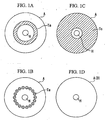
- a flat adhesive liquid film Tc is formed over almost the entire surface of the substrate except for a predetermined circular area having a central hole H in the center. Further, in Fig. 1D, the optical disc substrate A has no adhesive liquid film formed thereon.
- a combination with a substrate similar to the substrate A denoted in Fig. 1A or with any of the substrates A denoted in Figs. 1B to D can obtain the desired effect of the present invention by employing the voltage-applying method according to the present invention.
- the substrate A denoted in Fig. 1 B similarly, a combination with a substrate similar to the substrate A denoted in Fig. 1B or with any of the substrates A denoted in Fig.
- 1A to 1D can obtain the desired effect of the present invention by employing the voltage-applying method according to the present invention.
- a combination of the substrate A denoted in Fig. 1C and the substrate A denoted in Fig. 1D and a combination of the substrate A denoted in Fig. 1C and a substrate similar to the substrate A denoted in Fig. 1C cannot produce the desired effect of the present invention even by employing the voltage-applying method according to the present invention.
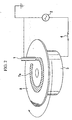
- Fig. 2 is a diagram for illustrating an embodiment in which a ring-shaped adhesive liquid film Ta as denoted in Fig. 1A is formed.
- An adhesive-supplying nozzle 1 for supplying a liquid adhesive to the optical disc substrate A is a small-diameter pipe made of an ordinary metallic material, by which a general liquid-supplying operation is performed.
- the adhesive-supplying nozzle 1 is connected to one of the terminals of an alternating-current power supply 2 as well as to the ground potential, and an electrode means 3 which serves as an electrode on a support stage is connected, via a switch 4, to the other terminal of the alternating-current power supply 2.
- the amount of the sinusoidal voltage applied cannot be generally determined because it depends on the rotation speed of the optical disc substrate A or the adhesive-supplying nozzle 1, the ejection speed of the liquid adhesive, and properties of the liquid adhesive such as resistivity and viscosity.
- the sinusoidal voltage having a peak value of about 1 kV and a frequency of 500 Hz was used.
- the amount of the sinusoidal voltage applied is preferably as small as possible in order to minimize the risk of occurrence of electrical discharge but large enough to achieve the desired object. It has been found that by setting the frequency of the applied sinusoidal voltage equal to 50 Hz and above when the ring-shaped adhesive liquid film Ta as denoted in Fig. 1A is formed, the amount of the applied sinusoidal voltage can be decreased while the desired object to prevent or reduce the formation of voids is achieved.
- the frequency of the sinusoidal voltage applied is preferably equal to 50 Hz and above.
- a base portion 5 which is made of a metallic material or a synthetic resin material whose surface is covered with an electrical insulating coating, has a ring-shaped peripheral wall portion 6 provided along the outermost periphery of one surface of the base portion for the purpose of storing an excess of the adhesive supplied from the adhesive-supplying nozzle 1.
- the adhesive-supplying nozzle 1 comprises a ring-shaped common nozzle portion 1a formed around the center of the base portion 5 and nozzle portions 1b formed at an approximately uniform spacing in the circumferential direction of the common nozzle portion 1a, and is made of a metal such as stainless steel.
- the numbers of the nozzle portions 1b are the same as the numbers of dots in the dot-shaped adhesive liquid films Tb as denoted in Fig. 1B for example.
- the base portion 5 has a liquid-supplying channel 7 for supplying a liquid adhesive to the adhesive-supplying nozzle 1.
- a support 9 is fixed which supports a center pin 8 which is inserted into the central hole H of the optical disc substrate A for positioning the optical disc substrate A.
- a support means 10 supports the optical disc substrate in order to move the optical disc substrate not only vertically but also horizontally as required, and comprises a ring-shaped plate or disc-shaped electrode portion 11 and a positioning means 12 which holds the center pin 8 on the main surface thereof.
- This support means 10 is connected to a driving mechanism for moving the optical disc substrate vertically or in other directions.
- a suction path and the like, for selectively holding the optical disc substrate by suction is formed on the underside of the electrode portion 11.
- the electrode portion 11 is connected, via the switch 4, to one of the terminals of the alternating-current power supply 2, and the adhesive-supplying nozzle 1 is connected not only to the ground potential but also to the other terminal of the alternating-current power supply 2.
- center pin 8 and the support 9 are not necessarily required, and it is also by all means acceptable to detect via a sensor (not shown) whether the support means 10 is moved horizontally to a predetermined position over the adhesive-supplying nozzle 1, in order to stop the horizontal movement and then move the support means 10 downward.
- the optical disc substrate A is stopped about 0.4 to 2 mm above the tips of the adhesive-supplying nozzle 1, and the liquid adhesive from the adhesive-supplying nozzle is applied to the underside of the optical disc substrate A, as exemplified by the substrate denoted in Fig. 1 B. Thereafter, the optical disc substrate A is brought upward and removed to proceed to the next step.
- an elastic material 9a is fixed on the upper surface of the support 9 to prevent the optical disc substrate A from approaching the tips of the adhesive-supplying nozzle 1 and further extends to a point about 0.4 mm away from the tips.
- the upper surface of the elastic material 9a is about 0.4 mm above the tips of the adhesive-supplying nozzle 1.
- the elastic material 9a serves as a stopper.
- the amount of applied sinusoidal voltage cannot be generally determined because the amount of applied sinusoidal voltage depends on the ejection speed of the liquid adhesive, properties of the liquid adhesive such as resistivity and viscosity, the capacitance between the electrodes, and the like.
- a sinusoidal voltage having a peak value of its about 400 V or higher is required.
- a sinusoidal voltage having a peak value of about 900 V and a frequency of 4 kHz or higher, and in consideration of the audio-frequency range, a sinusoidal voltage of 20 kHz was used
- the bonding of the optical disc substrate A to the optical disc substrate B will be described with reference to Figs. 1, 3, and 4 by considering the case where the optical disc substrate A is one having a ring-shaped adhesive liquid film as denoted in Fig. 1A, and the optical disc substrate B is one having no adhesive liquid film formed thereon as denoted in Fig. 1D
- the lower optical disc substrate A having the ring-shaped adhesive liquid film Ta as denoted in Fig. 1A is mounted on a support 15 of a bonding apparatus.
- the support 15 has a center axis 15A protruding at the center.
- the side wall of the center axis 15A is divided into a plurality of sections, through which chuck pawls, which will be described later, can pass.
- the support 15 has a ring-shaped electrode portion 16 to which one of the terminals of an alternating-current power supply 18 is connected via a power supply wire 17.
- the upper optical disc substrate B having no adhesive liquid film formed thereon is supported by a support means 19.
- the support means 19 is a disc-shaped member made of a conductive material such as stainless steel, which serves as one of the electrodes, and has a general suction mechanism (not shown) by which the support means 19 holds the upper surface of the upper optical disc substrate B by suction. Further, the support means 19 is connected to a transfer arm (not shown) that is horizontally spinnable at a certain angle and is electrically grounded through the transfer arm.
- a chuck means 20 having an axis whose center is aligned with the center of the center axis 15A of the support 15 is fixed.
- the chuck means 20 has three chuck pawls 20A which can change the diameter of the chuck means 20 by an external signal.
- the chuck pawls 20A expand the diameter in the central holes of the optical disc substrates A and B in order to hold the inner walls of the optical disc substrates A and B when the optical disc substrates A and B are transferred to another position while maintaining the substrate B on the substrate A.
- the support 15 is elevated by moving the lifting shaft 21 fixed on the underside of the support 15 upward by means of a driving mechanism (not shown) such as a cylinder device, whereby the spacing between the optical disc substrates A and B becomes smaller as denoted in Fig. 5A and the top of the liquid film Ta eventually makes contact with the underside of the optical disc substrate B as denoted in Fig. 5B.
- a driving mechanism such as a cylinder device
- the area of the top of the liquid film Ta at the moment when the liquid film Ta makes contact with the optical disc substrate B becomes significantly smaller than that of the prior art.
- the initial state of the contact is magnified and shown in Fig. 6.
- the liquid film Ta which makes contact with the optical disc substrate B spreads not only in the circumferential direction but also in the radial direction between the optical disc substrates A and B to form a circle as denoted in Figs. 5C and 5D.
- the chuck means 20 is operated by the external signal, and the chuck pawls 20A move to expand the diameter of the chuck means 20 in the central holes of the optical disc substrates A and B so as to hold the inner walls of the optical disc substrates A and B.
- the support 15 is brought down by moving the lifting shaft 21 downward, and the optical disc substrates A and B are held by the chuck means 20 and supported by the support means 19.
- the adhesive liquid film between the optical disc substrates A and B in this state spreads out much more widely than shown in Fig. 5, and minute voids or larger voids are not observed when the liquid film is observed through the optical disc substrates A and B.
- the support means 19 is spun by a spinning means (not shown) and transfers the optical disc substrates A and B to a spinner (not shown).
- the adhesive can make contact with the optical disc substrate B in a very preferable condition, and the formation of voids between the optical disc substrates A and B bonded together can be significantly inhibited.
- the optical disc substrates A and B are bonded together, it is difficult to make them sufficiently parallel to each other across the whole surface, and it is also extremely difficult to make the thickness of the adhesive liquid film Ta uniform. Therefore, when the adhesive liquid film Ta is observed microscopically at the time of contacting with the optical disc substrate B, the adhesive condition of the adhesive liquid film Ta is not actually uniform. Therefore, when a direct-current voltage is applied, the first portion of the liquid film which makes contact is wetted due to the effect of applying the voltage but the second and later portions of the liquid film which make contact are not ' ' wetted as well as the first portion.
- the electrode portion 16 of the support 15, the reflective film (not shown) of the optical disc substrate A and the insulating material of the optical disc substrate A form a first capacitance and exhibit an impedance Z1 as shown in Fig. 7.
- the gap between the reflective film of the optical disc substrate A and the reflective film (not shown) of the optical disc substrate B forms a second capacitance and exhibits an impedance Z2 as shown in Fig. 7.
- the reflective film of the optical disc substrate B, the support means 19 and the insulating material of the optical disc substrate B interposed between them form a third capacitance and exhibit an impedance Z3 as shown in Fig. 7.
- the gap between the reflective film of the optical disc substrate A and the reflective film of the optical disc substrate B is denoted by a switch S and the resistance of the adhesive is denoted by R; these are connected in parallel to the impedance Z2.
- the impedances Z1 to Z3 can be made small by applying a sinusoidal voltage having an appropriate frequency between the optical disc substrates A and B. Therefore, when the frequency f is determined such that the values of the impedances Z1 to Z3 are to be equal to or less than the resistance R of the adhesive, the voltage V2 between the reflective film of the optical disc substrate A and the reflective film of the optical disc substrate B is hardly affected by the resistance R.
- the sinusoidal voltage when the sinusoidal voltage is applied between the optical disc substrates A and B, by setting the frequency f of the sinusoidal voltage properly, the voltage V2 between the reflective film of the optical disc substrate A and the reflective film of the optical disc substrate B hardly decreases even when the adhesive liquid film Ta makes contact with the optical disc substrate B. This indicates that the effect of applying the voltage is still maintained even when a plurality of different portions of the adhesive liquid film Ta make contact at different times.
- the effect of applying the voltage is large when the frequency f of the sinusoidal voltage to be applied is 50 Hz or higher.
- the top of the liquid film Ta is tapered by the alternating-current electric field and the adhesive makes contact with the optical disc substrate B at the top, the occurrence of minute voids which are likely to be formed at the time of bonding is sufficiently inhibited. Further, since the liquid film Ta quickly spreads out not only in the circumferential direction but also in the radial direction between the optical disc substrates A and B whose surfaces are charged with positive and negative electric charges, no air is trapped therebetween in this process. Therefore, voids which are larger in diameter than the minute voids are also not formed in the adhesive layer which has been spread out thinly and uniformly between the optical disc substrates A and B by the spinning process.
- the voltage to be applied is a sinusoidal voltage
- voltage must be applied based on the mean value of the sinusoidal voltage since the absolute mean value affects the effect the voltage application.
- the waveform of the sinusoidal voltage is not limited to a sinusoidal wave and can be a positive and negative alternating waveform such as a rectangular wave, a trigonal wave or a sinusoidal wave having periods when the voltage is not applied.
- the present invention can be applied not only to the case where optical disc substrates are flat but also to the case where optical disc substrates having a curved surface, such as lenses, are bonded together, and the same effect can be obtained.
- two adhesive-supplying nozzles can be used which are separated from each other by 180 degrees and supply adhesives on the optical disc substrate simultaneously while the optical disc substrate is rotated about a half turn.
- the adhesive-supplying nozzle(s) can be rotated at a fixed speed.
- the same effect can be obtained by applying a direct-current voltage.
- the switch 4 is shown in Figs. 2 and 3 for illustrating the ON and OFF states of the sinusoidal voltage and is substituted with the switching element of the primary circuit of the alternating-current power supply in an actual apparatus.
Landscapes
- Engineering & Computer Science (AREA)
- Mechanical Engineering (AREA)
- Manufacturing & Machinery (AREA)
- Chemical & Material Sciences (AREA)
- Chemical Kinetics & Catalysis (AREA)
- General Chemical & Material Sciences (AREA)
- Manufacturing Optical Record Carriers (AREA)
- Lining Or Joining Of Plastics Or The Like (AREA)
- Adhesives Or Adhesive Processes (AREA)
Description
- The present invention relates to a method and an apparatus for forming a single optical disc substrate by bonding optical disc substrates together.
- When optical disc substrates are bonded together by an optical disc bonding apparatus using a liquid adhesive, it is important to ensure that no void exists in the adhesive layer after the bonding of the substrates. Therefore, various proposals have heretofore been considered, but all proposals have been unsatisfactory in that voids having a diameter of about 0.1 mm or larger, minute voids having a diameter of about 0.05 to 0.1 mm, or a mixture of these voids are formed between the optical disc substrates.
- As a method for significantly minimizing such a problem, the applicant of the present invention has applied the following invention, described in Japanese Patent Application No. Hei 10-257530. The invention will be described with reference to Fig. 8. Of two optical disc substrates A and B, a ring-shaped adhesive liquid film Ta is formed on the upper bonding surface of the lower optical disc substrate A. On the bonding surface of the upper optical disc substrate B, a plurality of dot-shaped adhesive liquid films Tb are formed in a circular shape having a diameter slightly larger than that of the ring-shaped adhesive liquid film Ta. Thereafter, the two optical disc substrates A and B are brought close together with the bonding surfaces thereof facing each other, and the two optical disc substrates A and B are joined together bringing the ring-shaped adhesive liquid film Ta into contact with the dot-shaped adhesive liquid films Tb. Then, the two optical disc substrates A and B are spin-processed to spread out the adhesive liquid film Ta and the adhesive liquid films Tb. The excess adhesive is spun off from the substrates, and an adhesive layer having a uniform films thickness is formed between the optical disc substrates A and B.
- In this method, by properly bringing the ends of the dot-shaped adhesive liquid films Tb, which are formed in a circular shape on the upper optical disc substrate B, into contact with the rim of the ring-shaped adhesive liquid film Ta formed on the lower optical disc substrate A, the development of particularly minute voids at the moment when these liquid films make contact with each other can be prevented. Further, since air between the liquid films is expelled when the contact portions between the liquid films expand over the entire liquid films, the occurrence of voids is lower at these points.
- However, since it is still extremely difficult, even by this method, to make the contact area sufficiently small at the moment when the adhesive liquid film Ta and the adhesive liquid films Tb contact each other, the development of minute voids cannot be totally prevented. Further, voids may develop when the adhesive liquid film Ta or the adhesive liquid films Tb make contact with the opposing optical disc substrate B or A.
- Further, since voids may also be formed when the adhesive liquid film Ta or the adhesive liquid films Tb are formed by supplying a liquid adhesive from an adhesive-supplying nozzle (not shown) onto the lower optical disc substrate A or onto the upper optical disc substrate B, the formation of voids during this process also needs to be prevented.
- Document EP-A-0 999 249 offers a process for avoiding the inclusion of bubbles during the joining by adhesives of optical data carrier substrates. It is proposed to apply an electrical charge through an electrical field to one and/or the other substrate and/or the adhesive.
- Document EF-A-1 026 214 discloses a system for avoiding voids in an adhesive layer sandwiched between two optical substrate discs. By applying an electric field during superposing the upper and lower plates, at least one being supplied with an adhesive, said adhesive is deformed into a tapered form, the initial contact form is reduced and then voids are reduced.
- The present invention has been invented in view of the above circumstances. The object of the present invention is to provide a method according to
claim 1 and an apparatus according to claim 11 for bonding optical disc substrates together, which rarely or never generate voids between the optical disc substrates when a liquid adhesive is supplied onto the optical disc substrate or the like, or when the two optical disc substrates or the like supplied with an adhesive are bonded together. - The present invention relates to a method for bonding two optical disc substrates together which comprises the steps of joining the optical disc substrates together with an adhesive and curing the adhesive, in which the adhesive is supplied onto the optical disc substrate by an electric field formed between an adhesive-supplying nozzle, for supplying the adhesive onto the optical disc substrate, and the optical disc substrate, and the two optical disc substrates are then joined together and spun by a spinning process.
- When the adhesive is supplied onto one of the two optical disc substrates in the shape of a ring, the other optical disc substrate may not have the adhesive applied thereon at all, may have the adhesive film formed over almost the entire surface, or may have the adhesive formed into dots at a relatively small spacing in a circular shape.
- When the adhesive is supplied as dots at a relatively small spacing in a circular shape on one of the two optical disc substrates, the other optical disc substrate may not have the adhesive applied thereon at all or may have the adhesive film formed over almost the entire surface.
- The present invention also relates to an apparatus for bonding optical disc substrates together by joining the two optical disc substrates together with an adhesive and curing the adhesive, which comprises an adhesive-supplying nozzle for supplying the adhesive onto the optical disc substrate, an electrode means placed in contact with or in the vicinity of the surface of the optical disc substrate which is opposite the surface which faces the adhesive-supplying nozzle, and an electric power supply for generating an electric field between the electrode means and the adhesive-supplying nozzle.
- The adhesive-supplying nozzle comprises a single nozzle or two nozzles separated from each other by almost 180 degrees, is placed over the optical disc substrate nearly perpendicular thereto with its tip(s) pointing downward, and forms a ring-shaped adhesive liquid film on the optical disc substrate which spins relative to the nozzle(s).
- The adhesive-supplying nozzle may comprise, for example, a plurality of nozzles placed at an approximately uniform spacing in a circular shape, may be placed under the optical disc substrate nearly perpendicular thereto with their tips pointing upward, and may supply dot-shaped adhesive liquid films onto the underside of the optical disc substrate.
- In this case, the electric field generated by the electric power supply may be an alternating-current or a direct-current electric field. However, the alternating-current electric field is preferable.
-
- Fig. 1A is a front view of optical disc substrate which illustrates an embodiment of the method for bonding optical disc substrates of the present invention.
- Fig. 1B is a front view of optical disc substrate which illustrates an embodiment of the method for bonding optical disc substrates of the present invention.
- Fig. 1C is a front view of optical disc substrate which illustrates an embodiment of the method for bonding optical disc substrates of the present invention.
- Fig. 1D is a front view of optical disc substrate which illustrates an embodiment of the method for bonding optical disc substrates of the present invention.
- Fig. 2 is an upper perspective view which illustrates an embodiment of the method and the apparatus for bonding optical disc substrates together according to the present invention.
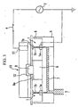
- Fig. 3 is a cross-sectional view which illustrates an embodiment of the method and the apparatus for bonding optical disc substrates together according to the present invention.
- Fig. 4 is a cross-sectional view which illustrates an embodiment of the method and the apparatus for bonding optical disc substrates together according to the present invention.
- Fig. 5A is a front view and a side view of optical disc substrates which stepwise illustrates an embodiment for bonding optical disc substrates together according to the present invention.
- Fig. 5B is a front view and a side view of optical disc substrates which stepwise illustrates an embodiment for bonding optical disc substrates together according to the present invention.
- Fig. 5C is a front view and a side view of optical disc substrates which stepwise illustrates an embodiment for bonding optical disc substrates together according to the present invention.
- Fig. 5D is a front view and a side view of optical disc substrates which stepwise illustrates an embodiment for bonding optical disc substrates together according to the present invention.
- Fig. 6 is a front view and a side view of optical disc substrates which illustrate an embodiment for bonding optical disc substrates together according to the present invention.
- Fig. 7 is a circuit diagram which illustrates an embodiment for bonding of optical ' disc substrates together according to the present invention.
- Fig. 8 is a front view and a sectional view of optical disc substrates which illustrates a conventional method for bonding optical disc substrates together.
- A description of the principle of the present invention will first be given. The present invention is based on a finding that when an electric field, especially an alternating-current electric field, is generated between an adhesive-supplying nozzle and an optical disc substrate at the time of supplying a liquid adhesive from the adhesive-supplying nozzle onto the optical disc substrate, a contact area of the liquid film of the adhesive supplied onto the optical disc substrate which makes contact with the other optical disc substrate directly or when the adhesive liquid film is formed thereon for the first time, can be smaller, and the less likely it is that voids are formed in compliance with the contact area is smaller.
- It is believed that because the electric field becomes quite large immediately before the liquid film of the adhesive first makes contact, an end of the liquid film of the adhesive is tapered off, thereby making the contact area smaller.
- Generally known digital versatile discs (DVD) are classified into: a single-sided single-layer optical disc in which only one of the optical disc substrates to be bonded together has a recording layer comprising pits and a reflective layer; a double-sided single-layer optical disc in which both of the optical disc substrates to be bonded together have a recording layer; a single-sided double-layer optical disc in which the reflective layer of one of the optical disc substrates to be bonded together is a translucent film; a combination of the single-sided single-layer optical disc and the single-sided double-layer optical disc described above; and a double-sided double-layer optical disc comprising two single-sided double-layer optical discs bonded together. The present invention can be applied to the production of any of these various types of DVD's.
- Before a description of the embodiments of the present invention is given to, the shapes and combinations of liquid adhesives on an optical disc substrate from which the desired effects can be expected when the present invention is applied will be described by taking an optical disc substrate having a hole in the center as an example. In Fig. 1A, on the optical disc substrate denoted by the mark A, an adhesive liquid film Ta is formed in the shape of a ring around a central hole H. In Fig. 1B, on the optical disc substrate A, dot-shaped adhesive liquid films Tb are formed into dots at a small spacing in a circular shape having a central hole H in the center. In Fig. 1C, on the optical disc substrate A, a flat adhesive liquid film Tc is formed over almost the entire surface of the substrate except for a predetermined circular area having a central hole H in the center. Further, in Fig. 1D, the optical disc substrate A has no adhesive liquid film formed thereon.
- Next, combinations of the substrates A denoted in Figs. 1A to 1D, with which the effect of the present invention can be obtained, will be described. As for the substrate A denoted in Fig. 1 A, a combination with a substrate similar to the substrate A denoted in Fig. 1A or with any of the substrates A denoted in Figs. 1B to D can obtain the desired effect of the present invention by employing the voltage-applying method according to the present invention. As for the substrate A denoted in Fig. 1 B, similarly, a combination with a substrate similar to the substrate A denoted in Fig. 1B or with any of the substrates A denoted in Fig. 1A to 1D can obtain the desired effect of the present invention by employing the voltage-applying method according to the present invention. On the other hand, a combination of the substrate A denoted in Fig. 1C and the substrate A denoted in Fig. 1D and a combination of the substrate A denoted in Fig. 1C and a substrate similar to the substrate A denoted in Fig. 1C cannot produce the desired effect of the present invention even by employing the voltage-applying method according to the present invention.
- A description of the first embodiment of the present invention will be given to a with reference to the drawings.
- Fig. 2 is a diagram for illustrating an embodiment in which a ring-shaped adhesive liquid film Ta as denoted in Fig. 1A is formed. An adhesive-supplying
nozzle 1 for supplying a liquid adhesive to the optical disc substrate A is a small-diameter pipe made of an ordinary metallic material, by which a general liquid-supplying operation is performed. The adhesive-supplyingnozzle 1 is connected to one of the terminals of an alternating-current power supply 2 as well as to the ground potential, and an electrode means 3 which serves as an electrode on a support stage is connected, via aswitch 4, to the other terminal of the alternating-current power supply 2. Therefore, when theswitch 4 is ON and a sinusoidal voltage from the alternating-current power supply 2 is applied between the adhesive-supplyingnozzle 1 and the electrode means 3, an alternating-current electric field is generated therebetween. By continuously supplying a predetermined amount of a liquid adhesive from the adhesive-supplyingnozzle 1 onto the bonding surface of the disc substrate A while the support stage is rotated almost 360° at a fixed speed while the alternating-current electric field is generated, a ring-shaped adhesive liquid film Ta as denoted in Fig. 1A is formed. In this case, end of the liquid film of the adhesive is tapered off due to the effect of the alternating-current electric field and the contact area becomes smaller, whereby voids are less likely to be formed between the optical disc substrate A and the liquid film Ta. - The amount of the sinusoidal voltage applied cannot be generally determined because it depends on the rotation speed of the optical disc substrate A or the adhesive-supplying
nozzle 1, the ejection speed of the liquid adhesive, and properties of the liquid adhesive such as resistivity and viscosity. In the embodiment, the sinusoidal voltage having a peak value of about 1 kV and a frequency of 500 Hz was used. In this case, the amount of the sinusoidal voltage applied is preferably as small as possible in order to minimize the risk of occurrence of electrical discharge but large enough to achieve the desired object. It has been found that by setting the frequency of the applied sinusoidal voltage equal to 50 Hz and above when the ring-shaped adhesive liquid film Ta as denoted in Fig. 1A is formed, the amount of the applied sinusoidal voltage can be decreased while the desired object to prevent or reduce the formation of voids is achieved. Thus, the frequency of the sinusoidal voltage applied is preferably equal to 50 Hz and above. - Next, an embodiment, in which dot-shaped adhesive liquid films Tb as denoted in Fig. 1B are formed, will be described with reference to Fig. 3. A
base portion 5 which is made of a metallic material or a synthetic resin material whose surface is covered with an electrical insulating coating, has a ring-shaped peripheral wall portion 6 provided along the outermost periphery of one surface of the base portion for the purpose of storing an excess of the adhesive supplied from the adhesive-supplyingnozzle 1. The adhesive-supplyingnozzle 1 comprises a ring-shapedcommon nozzle portion 1a formed around the center of thebase portion 5 andnozzle portions 1b formed at an approximately uniform spacing in the circumferential direction of thecommon nozzle portion 1a, and is made of a metal such as stainless steel. The numbers of thenozzle portions 1b are the same as the numbers of dots in the dot-shaped adhesive liquid films Tb as denoted in Fig. 1B for example. Further, thebase portion 5 has a liquid-supplying channel 7 for supplying a liquid adhesive to the adhesive-supplyingnozzle 1. At the center of thebase portion 5, asupport 9 is fixed which supports acenter pin 8 which is inserted into the central hole H of the optical disc substrate A for positioning the optical disc substrate A. - A support means 10 supports the optical disc substrate in order to move the optical disc substrate not only vertically but also horizontally as required, and comprises a ring-shaped plate or disc-shaped electrode portion 11 and a positioning means 12 which holds the
center pin 8 on the main surface thereof. This support means 10 is connected to a driving mechanism for moving the optical disc substrate vertically or in other directions. Further, although not shown, a suction path and the like, for selectively holding the optical disc substrate by suction, is formed on the underside of the electrode portion 11. The electrode portion 11 is connected, via theswitch 4, to one of the terminals of the alternating-current power supply 2, and the adhesive-supplyingnozzle 1 is connected not only to the ground potential but also to the other terminal of the alternating-current power supply 2. Further, thecenter pin 8 and thesupport 9 are not necessarily required, and it is also by all means acceptable to detect via a sensor (not shown) whether the support means 10 is moved horizontally to a predetermined position over the adhesive-supplyingnozzle 1, in order to stop the horizontal movement and then move the support means 10 downward. - In the case of forming the liquid films Tb, when the support means 10 holds the optical disc substrate A by suction at the different position from the position shown in Fig. 3, the support means 10 moves upper area of the illustration shown in Fig. 3 and then starts to move downward. By flipping the
switch 4 ON during this process, the sinusoidal voltage from the alternating-current power supply 2 is applied to the whole adhesive-supplyingnozzle 1 and the electrode portion 11 of the support means 10, and thereby an alternating-current electric field is generated between them. When the alternating-current electric field is generated, the optical disc substrate A is stopped about 0.4 to 2 mm above the tips of the adhesive-supplyingnozzle 1, and the liquid adhesive from the adhesive-supplying nozzle is applied to the underside of the optical disc substrate A, as exemplified by the substrate denoted in Fig. 1 B. Thereafter, the optical disc substrate A is brought upward and removed to proceed to the next step. Incidentally, as a safety measure, anelastic material 9a is fixed on the upper surface of thesupport 9 to prevent the optical disc substrate A from approaching the tips of the adhesive-supplyingnozzle 1 and further extends to a point about 0.4 mm away from the tips. The upper surface of theelastic material 9a is about 0.4 mm above the tips of the adhesive-supplyingnozzle 1. In other words, theelastic material 9a serves as a stopper. - When a liquid adhesive is applied from the adhesive-supplying
nozzle 1 to the underside of the optical disc substrate A when the alternating-current electric field is generated described above, the intensity of the alternating-current electric field becomes relatively high because the spacing between the adhesive-supplyingnozzle 1 and the electrode portion 11 of the support means 10 becomes very small. As a result, when viewed microscopically, immediately before application, the adhesive at the end of the adhesive-supplyingnozzle 1 tapers off upward, and the contact area at the time of first making contact with the optical disc substrate A is sufficiently small. This is the reason why voids are rarely formed. As a result, an adhesive liquid film can be obtained having the pattern as denoted in Fig. 1B, in which substantially no voids are formed even by the method and apparatus presented in the present embodiment. - In the present embodiment as well, the amount of applied sinusoidal voltage cannot be generally determined because the amount of applied sinusoidal voltage depends on the ejection speed of the liquid adhesive, properties of the liquid adhesive such as resistivity and viscosity, the capacitance between the electrodes, and the like. However, a sinusoidal voltage having a peak value of its about 400 V or higher is required. In the present embodiment, a sinusoidal voltage having a peak value of about 900 V and a frequency of 4 kHz or higher, and in consideration of the audio-frequency range, a sinusoidal voltage of 20 kHz was used
- Next, the bonding of the optical disc substrate A to the optical disc substrate B will be described with reference to Figs. 1, 3, and 4 by considering the case where the optical disc substrate A is one having a ring-shaped adhesive liquid film as denoted in Fig. 1A, and the optical disc substrate B is one having no adhesive liquid film formed thereon as denoted in Fig. 1D
- The lower optical disc substrate A having the ring-shaped adhesive liquid film Ta as denoted in Fig. 1A is mounted on a
support 15 of a bonding apparatus. Thesupport 15 has a center axis 15A protruding at the center. The side wall of the center axis 15A is divided into a plurality of sections, through which chuck pawls, which will be described later, can pass. Further, thesupport 15 has a ring-shapedelectrode portion 16 to which one of the terminals of an alternating-current power supply 18 is connected via apower supply wire 17. Meanwhile, the upper optical disc substrate B having no adhesive liquid film formed thereon is supported by a support means 19. The support means 19 is a disc-shaped member made of a conductive material such as stainless steel, which serves as one of the electrodes, and has a general suction mechanism (not shown) by which the support means 19 holds the upper surface of the upper optical disc substrate B by suction. Further, the support means 19 is connected to a transfer arm (not shown) that is horizontally spinnable at a certain angle and is electrically grounded through the transfer arm. - At the center of the support means 19, a chuck means 20 having an axis whose center is aligned with the center of the center axis 15A of the
support 15 is fixed. The chuck means 20 has threechuck pawls 20A which can change the diameter of the chuck means 20 by an external signal. The chuck pawls 20A expand the diameter in the central holes of the optical disc substrates A and B in order to hold the inner walls of the optical disc substrates A and B when the optical disc substrates A and B are transferred to another position while maintaining the substrate B on the substrate A. - The operation of this mechanism will be described with reference to Figs. 5 and 6 in addition to the above Figs. 1 to 4. The lower optical disc substrate A is mounted on the
support 15, and in this state, the continuous ring-shaped liquid film Ta is formed on the upper surface of the optical disc substrate A as described in the above embodiment. Then, when the optical disc substrates A and B are opposite each other, a sinusoidal voltage is applied between theelectrode portion 16 of thesupport 15 and the support means 19 by the alternating-current power supply 18 to generate an alternating-current electric field between the optical disc substrates A and B. Next, thesupport 15 is elevated by moving the liftingshaft 21 fixed on the underside of thesupport 15 upward by means of a driving mechanism (not shown) such as a cylinder device, whereby the spacing between the optical disc substrates A and B becomes smaller as denoted in Fig. 5A and the top of the liquid film Ta eventually makes contact with the underside of the optical disc substrate B as denoted in Fig. 5B. During this approaching process of the liquid film Ta, since the intensity of the electric field between the optical disc substrates A and B becomes stronger as the spacing between them becomes smaller, the top of the liquid film Ta tapers off upward by suction force caused by the electric field, and the tapered top of the liquid film Ta makes contact with the underside of the optical disc substrate B first. Therefore, the area of the top of the liquid film Ta at the moment when the liquid film Ta makes contact with the optical disc substrate B becomes significantly smaller than that of the prior art. The initial state of the contact is magnified and shown in Fig. 6. The liquid film Ta which makes contact with the optical disc substrate B spreads not only in the circumferential direction but also in the radial direction between the optical disc substrates A and B to form a circle as denoted in Figs. 5C and 5D. - Next, the chuck means 20 is operated by the external signal, and the
chuck pawls 20A move to expand the diameter of the chuck means 20 in the central holes of the optical disc substrates A and B so as to hold the inner walls of the optical disc substrates A and B. With this state maintained, thesupport 15 is brought down by moving the liftingshaft 21 downward, and the optical disc substrates A and B are held by the chuck means 20 and supported by the support means 19. In reality, the adhesive liquid film between the optical disc substrates A and B in this state spreads out much more widely than shown in Fig. 5, and minute voids or larger voids are not observed when the liquid film is observed through the optical disc substrates A and B. Thereafter, the support means 19 is spun by a spinning means (not shown) and transfers the optical disc substrates A and B to a spinner (not shown). - That is, in the present embodiment, since an electric field is generated when the liquid adhesive is supplied onto the optical disc substrate A or when the optical disc substrates A and B are bonded together, the adhesive can make contact with the optical disc substrate B in a very preferable condition, and the formation of voids between the optical disc substrates A and B bonded together can be significantly inhibited.
- When the optical disc substrates A and B are bonded together, it is difficult to make them sufficiently parallel to each other across the whole surface, and it is also extremely difficult to make the thickness of the adhesive liquid film Ta uniform. Therefore, when the adhesive liquid film Ta is observed microscopically at the time of contacting with the optical disc substrate B, the adhesive condition of the adhesive liquid film Ta is not actually uniform. Therefore, when a direct-current voltage is applied, the first portion of the liquid film which makes contact is wetted due to the effect of applying the voltage but the second and later portions of the liquid film which make contact are not ' ' wetted as well as the first portion. This is because the positive and negative electric charges induced between the optical disc substrates A and B through the resistance R (to be described later) of the adhesive start to neutralize from the moment when the first portion of the liquid film makes contact, whereby the voltage between the optical disc substrates A and B decreases and the effect of applying the voltage is therefore weakened to some extent. Thus, the sinusoidal voltage was applied in the present embodiment.
- When the sinusoidal voltage is applied, the
electrode portion 16 of thesupport 15, the reflective film (not shown) of the optical disc substrate A and the insulating material of the optical disc substrate A form a first capacitance and exhibit an impedance Z1 as shown in Fig. 7. The gap between the reflective film of the optical disc substrate A and the reflective film (not shown) of the optical disc substrate B forms a second capacitance and exhibits an impedance Z2 as shown in Fig. 7. Further, the reflective film of the optical disc substrate B, the support means 19 and the insulating material of the optical disc substrate B interposed between them form a third capacitance and exhibit an impedance Z3 as shown in Fig. 7. Furthermore, in Fig. 7, the gap between the reflective film of the optical disc substrate A and the reflective film of the optical disc substrate B is denoted by a switch S and the resistance of the adhesive is denoted by R; these are connected in parallel to the impedance Z2. - Since all of the impedances Z1 to Z3 tend to become small in response to an increase in the frequency f of a voltage to be applied (for example, Z1 = 1/2πfC3 and Z3 = 1/2πfC1, on the proviso that Z1 and Z3 are absolute values), the impedances Z1 to Z3 can be made small by applying a sinusoidal voltage having an appropriate frequency between the optical disc substrates A and B. Therefore, when the frequency f is determined such that the values of the impedances Z1 to Z3 are to be equal to or less than the resistance R of the adhesive, the voltage V2 between the reflective film of the optical disc substrate A and the reflective film of the optical disc substrate B is hardly affected by the resistance R.
- That is, when the sinusoidal voltage is applied between the optical disc substrates A and B, by setting the frequency f of the sinusoidal voltage properly, the voltage V2 between the reflective film of the optical disc substrate A and the reflective film of the optical disc substrate B hardly decreases even when the adhesive liquid film Ta makes contact with the optical disc substrate B. This indicates that the effect of applying the voltage is still maintained even when a plurality of different portions of the adhesive liquid film Ta make contact at different times.
- In this case, when conditions such as the thicknesses of the optical disc substrates A and B, the dielectric constants and the resistivity of the adhesive are taken into consideration, the effect of applying the voltage is large when the frequency f of the sinusoidal voltage to be applied is 50 Hz or higher.
- According to the present embodiment, since the top of the liquid film Ta is tapered by the alternating-current electric field and the adhesive makes contact with the optical disc substrate B at the top, the occurrence of minute voids which are likely to be formed at the time of bonding is sufficiently inhibited. Further, since the liquid film Ta quickly spreads out not only in the circumferential direction but also in the radial direction between the optical disc substrates A and B whose surfaces are charged with positive and negative electric charges, no air is trapped therebetween in this process. Therefore, voids which are larger in diameter than the minute voids are also not formed in the adhesive layer which has been spread out thinly and uniformly between the optical disc substrates A and B by the spinning process. Further, when the voltage to be applied is a sinusoidal voltage, voltage must be applied based on the mean value of the sinusoidal voltage since the absolute mean value affects the effect the voltage application. Further, the waveform of the sinusoidal voltage is not limited to a sinusoidal wave and can be a positive and negative alternating waveform such as a rectangular wave, a trigonal wave or a sinusoidal wave having periods when the voltage is not applied.
- Further, when the substrates denoted in Fig. 1A are bonded together, when the substrate denoted in Fig. 1A, 1C or 1D are bonded together, or even when the substrate denoted in Fig. 1B and the substrate denoted in Fig. 1A, 1C or 1D are bonded together, ' the present invention can be applied to these cases exactly in the same manner as in the present embodiment, and the same effect can be obtained. Thus, descriptions therefor will be omitted.
- Further, the present invention can be applied not only to the case where optical disc substrates are flat but also to the case where optical disc substrates having a curved surface, such as lenses, are bonded together, and the same effect can be obtained. Further, although the case where a single adhesive-supplying nozzle is used has been described in the embodiment shown in Fig. 2, two adhesive-supplying nozzles can be used which are separated from each other by 180 degrees and supply adhesives on the optical disc substrate simultaneously while the optical disc substrate is rotated about a half turn. Further, instead of the optical disc substrate, the adhesive-supplying nozzle(s) can be rotated at a fixed speed. Still further, there is also a case where the same effect can be obtained by applying a direct-current voltage. Incidentally, the
switch 4 is shown in Figs. 2 and 3 for illustrating the ON and OFF states of the sinusoidal voltage and is substituted with the switching element of the primary circuit of the alternating-current power supply in an actual apparatus.
Claims (16)
- A method for bonding two optical disc substrates together which comprises the steps of joining the optical disc substrates together with an adhesive and curing the adhesive, wherein the adhesive is supplied onto at least one of the optical disc substrates by an electric field formed between an adhesive-supplying nozzle, for supplying the adhesive onto the optical disc substrate, and the optical disc substrate, and the two optical disc substrates are then joined together and subjected to SPIN by a spinning process.
- The method for bonding two optical disc substrates together of claim 1, wherein the adhesive is supplied onto one of the two optical disc substrates in the shape of a ring and is not supplied onto the other optical disc substrate.
- The method for bonding two optical disc substrates together of claim 1, wherein the adhesive is supplied onto one of the two optical disc substrates in the shape of a ring and is formed over almost the entire surface of the other optical disc substrate
- The method for bonding two optical disc substrates together of claim 1, wherein the adhesive is supplied onto one of the two optical disc substrates in the shape of a ring and is supplied as dots at a relatively small spacing in a circular shape onto the other optical disc substrate.
- The method for bonding two optical disc substrates together of claim 1, wherein the adhesive is supplied as dots at a relatively small spacing in a circular shape onto one of the two optical disc substrates and is not supplied onto the other optical disc substrate.
- The method for bonding two optical disc substrates together of claim 1, wherein the adhesive is supplied as dots in a circular shape onto one of the two optical disc substrates and is formed over almost the entire surface of the other optical disc substrate.
- The method for bonding two optical disc substrates together according to any one of claims 1 to 6, wherein the electric field is an alternating-current electric field.
- The method for bonding two optical disc substrates together according to any one of claims 1 to 6, wherein the electric field is a direct-current electric field.
- The method for bonding two optical disc substrates together of claim 1, wherein the adhesive is supplied onto the optical disc substrate by the electric field formed between the adhesive-supplying nozzle and the optical disc substrate, so as to taper an end of the liquid film of the adhesive toward the optical disc substrate in order to reduce an initial contact area between said end of the liquid film of the adhesive and the optical disc substrate for preventing generation of voids in said adhesive.
- The method for bonding two optical disc substrates together of claim 1, wherein the two optical disc substrates are joined together with said adhesive while forming an electric field between said two optical disc substrates so as to taper an end of the liquid film of said adhesive toward the opposite optical disc substrate.
- An apparatus for bonding two optical disc substrates together by joining the optical disc substrates together with an adhesive and by curing the adhesive, which comprises an adhesive-supplying nozzle for supplying the adhesive onto at least one of the optical disc substrates, an electrode means placed in contact with or in the vicinity of the surface of the optical disc substrate which is opposite to the surface which faces the adhesive-supplying nozzle, and an electric power supply for generating an electric field between the electrode means and the adhesive-supplying nozzle.
- The apparatus for bonding two optical disc substrates together according to claim 11,• wherein the adhesive-supplying nozzle comprises a single nozzle or two nozzles placed separated from each other by almost 180 degrees away from each other,• wherein the adhesive-supplying nozzle is placed over the optical disc substrate nearly perpendicular thereto with its tip(s) pointing downward,• and wherein the adhesive-supplying nozzle forms a ring-shaped adhesive liquid film on the optical disc substrate which spins relative to the nozzle(s).
- The apparatus for bonding two optical disc substrates together according to claim 11,• wherein the adhesive-supplying nozzle comprises a plurality of nozzles placed at an approximately uniform spacing in a circular shape,• wherein the adhesive-supplying nozzle is placed under the optical disc substrate nearly perpendicular thereto with their tips pointing upward,• and wherein the adhesive-supplying nozzle supplies dot-shaped adhesive liquid films onto the underside of the optical disc substrate.
- The apparatus for bonding two optical disc substrates together according to any one of claims 11 to 13, wherein the electric power supply generates an alternating-current electric field.
- The apparatus for bonding two optical disc substrates together according to any one of claims 11 to 13, wherein the electric power supply generates a direct-current electric field.
- The apparatus for bonding two optical disc substrates together according to claim 11, wherein the electric power supply generates the electric field between the electrode means and the adhesive-supplying nozzle, so as to taper an end of the liquid film of the adhesive toward the optical disc substrate in order to reduce an initial contact area between said end of the liquid film of the adhesive and the optical disc substrate for preventing generation of voids in said adhesive.
Priority Applications (1)
| Application Number | Priority Date | Filing Date | Title |
|---|---|---|---|
| EP20060300051 EP1656999B1 (en) | 2000-04-27 | 2001-02-06 | Method for supplying liquid material |
Applications Claiming Priority (2)
| Application Number | Priority Date | Filing Date | Title |
|---|---|---|---|
| JP2000127061 | 2000-04-27 | ||
| JP2000127061A JP3516632B2 (en) | 2000-04-27 | 2000-04-27 | Method and apparatus for bonding optical disk substrates |
Related Child Applications (1)
| Application Number | Title | Priority Date | Filing Date |
|---|---|---|---|
| EP20060300051 Division EP1656999B1 (en) | 2000-04-27 | 2001-02-06 | Method for supplying liquid material |
Publications (3)
| Publication Number | Publication Date |
|---|---|
| EP1152408A2 EP1152408A2 (en) | 2001-11-07 |
| EP1152408A3 EP1152408A3 (en) | 2003-02-26 |
| EP1152408B1 true EP1152408B1 (en) | 2006-11-08 |
Family
ID=18636728
Family Applications (2)
| Application Number | Title | Priority Date | Filing Date |
|---|---|---|---|
| EP20060300051 Expired - Lifetime EP1656999B1 (en) | 2000-04-27 | 2001-02-06 | Method for supplying liquid material |
| EP20010420027 Expired - Lifetime EP1152408B1 (en) | 2000-04-27 | 2001-02-06 | Method and apparatus for bonding optical disc substrates together |
Family Applications Before (1)
| Application Number | Title | Priority Date | Filing Date |
|---|---|---|---|
| EP20060300051 Expired - Lifetime EP1656999B1 (en) | 2000-04-27 | 2001-02-06 | Method for supplying liquid material |
Country Status (8)
| Country | Link |
|---|---|
| US (2) | US6685794B2 (en) |
| EP (2) | EP1656999B1 (en) |
| JP (1) | JP3516632B2 (en) |
| KR (1) | KR100562217B1 (en) |
| CN (1) | CN100437789C (en) |
| DE (1) | DE60124338T2 (en) |
| HK (1) | HK1041553B (en) |
| TW (1) | TW518592B (en) |
Families Citing this family (14)
| Publication number | Priority date | Publication date | Assignee | Title |
|---|---|---|---|---|
| TW459225B (en) * | 1999-02-01 | 2001-10-11 | Origin Electric | Bonding system and method |
| US20080283192A1 (en) * | 2000-04-27 | 2008-11-20 | Shinichi Shinohara | Method and apparatus for bonding optical disc substrates together, and method for supplying liquid material |
| JP2003067991A (en) * | 2001-06-07 | 2003-03-07 | Fuji Photo Film Co Ltd | Optical disc manufacturing method and disc stack conveying method |
| DE10243663B4 (en) * | 2002-09-20 | 2007-10-11 | Krauss-Maffei Kunststofftechnik Gmbh | Method and device for the production of glued plates |
| AU2002332988A1 (en) * | 2002-10-24 | 2004-05-13 | Crushing And Mining Equipment Pty Ltd | A distributor plate |
| US20070082179A1 (en) * | 2005-10-07 | 2007-04-12 | Wade James J | Method and apparatus for forming optical articles |
| CN100587822C (en) * | 2005-12-26 | 2010-02-03 | 东莞宏威数码机械有限公司 | Apparatus and method for producing optical recording medium |
| CN100509386C (en) * | 2005-12-26 | 2009-07-08 | 东莞宏威数码机械有限公司 | Apparatus and method for manufacturing optical recording medium |
| CN100467266C (en) * | 2005-12-26 | 2009-03-11 | 东莞宏威数码机械有限公司 | Bonding method and apparatus for manufacturing DVD optical disk |
| US9884475B2 (en) * | 2011-01-19 | 2018-02-06 | Precision Valve & Automation, Inc. | Machine for optical bonding, system and method of use thereof |
| US8608896B2 (en) | 2011-09-13 | 2013-12-17 | Apple Inc. | Liquid adhesive lamination for precision adhesive control |
| JP5902524B2 (en) * | 2012-03-23 | 2016-04-13 | 東北パイオニアEg株式会社 | Substrate bonding method and bonding apparatus |
| WO2015137042A1 (en) * | 2014-03-14 | 2015-09-17 | オリジン電気株式会社 | Resin coater and method for manufacturing resin-coated component |
| FR3088353B1 (en) * | 2018-11-14 | 2022-07-15 | Rubberflex | FLAT ROOF RAINWATER DRAINAGE UNIT AND ASSOCIATED METHODS |
Family Cites Families (31)
| Publication number | Priority date | Publication date | Assignee | Title |
|---|---|---|---|---|
| DE2361762C3 (en) * | 1973-12-12 | 1980-04-17 | Philips Patentverwaltung Gmbh, 2000 Hamburg | Writing device for punctiform selective transfer of liquid color |
| US4727296A (en) * | 1983-08-25 | 1988-02-23 | Lutron Electronics Co., Inc. | Lighting scene control panel and control circuit |
| JPS61235133A (en) | 1985-04-11 | 1986-10-20 | Ricoh Co Ltd | Manufacture of information record carrier |
| JPH0736901B2 (en) | 1986-02-25 | 1995-04-26 | 富士写真フイルム株式会社 | Coating method and device |
| JPH069671B2 (en) * | 1986-06-25 | 1994-02-09 | 富士写真フイルム株式会社 | Application method |
| GB8617527D0 (en) * | 1986-07-17 | 1986-08-28 | Ici Plc | Spraying process |
| JPS6414752A (en) | 1987-07-09 | 1989-01-18 | Seiko Epson Corp | Production of optical recording medium |
| DE3866043D1 (en) * | 1987-07-23 | 1991-12-12 | Asahi Glass Co Ltd | FIELD GENERATION DEVICE. |
| JP2681488B2 (en) * | 1988-07-04 | 1997-11-26 | ティーディーケイ株式会社 | Stamper surface treatment method |
| JPH04170731A (en) | 1990-11-01 | 1992-06-18 | Matsushita Electric Ind Co Ltd | Antistatic optical disc substrate |
| JPH0536118A (en) | 1991-07-31 | 1993-02-12 | Sharp Corp | Optical disk manufacturing method |
| JPH07228847A (en) * | 1994-02-15 | 1995-08-29 | Ricoh Co Ltd | Adhesive and bonding method |
| JPH0836791A (en) * | 1994-07-25 | 1996-02-06 | Mitsubishi Chem Corp | Manufacturing method of optical disk with sliding film |
| US5935331A (en) * | 1994-09-09 | 1999-08-10 | Matsushita Electric Industrial Co., Ltd. | Apparatus and method for forming films |
| JPH08293132A (en) * | 1995-04-20 | 1996-11-05 | Kitano Eng Kk | Optical disc manufacturing method |
| JPH09138976A (en) * | 1995-11-17 | 1997-05-27 | Nec Corp | Information recording medium and method of manufacturing the same |
| JPH09265673A (en) * | 1996-03-25 | 1997-10-07 | Meiki Co Ltd | Laminated disc product substrate laminating method |
| CN1306509C (en) * | 1996-04-19 | 2007-03-21 | 松下电器产业株式会社 | Method and device for manufacturing laminated optical disc |
| SE506616C2 (en) * | 1996-05-13 | 1998-01-19 | Toolex Alpha Ab | Bonding nozzle for bonding optical disc elements |
| JP3684775B2 (en) * | 1997-07-23 | 2005-08-17 | ソニー株式会社 | Optical recording medium manufacturing method and manufacturing apparatus therefor |
| JP4068187B2 (en) | 1997-08-25 | 2008-03-26 | 松下電器産業株式会社 | Optical disc manufacturing method |
| JPH11120631A (en) * | 1997-10-15 | 1999-04-30 | Nikon Corp | Optical disc manufacturing method |
| DE19748699A1 (en) | 1997-11-04 | 1999-05-06 | Data Disc Robots Gmbh | Process for gluing data carrier disks |
| EP0919288A3 (en) * | 1997-11-25 | 2003-10-08 | Nordson Corporation | Electrostatic dispensing apparatus and method |
| JPH11224444A (en) * | 1998-02-04 | 1999-08-17 | Kao Corp | Optical disc manufacturing method |
| JP3725344B2 (en) * | 1998-05-11 | 2005-12-07 | オリジン電気株式会社 | Optical disk laminating method and apparatus |
| DE19850832C5 (en) * | 1998-11-04 | 2005-10-06 | Singulus Technologies Ag | Method for connecting substrate halves of optical data carriers |
| JP3177969B2 (en) | 1998-12-07 | 2001-06-18 | 日本電気株式会社 | Semiconductor substrate spin coating apparatus and spin coating method |
| TW459225B (en) * | 1999-02-01 | 2001-10-11 | Origin Electric | Bonding system and method |
| JP3312731B2 (en) | 1999-02-01 | 2002-08-12 | オリジン電気株式会社 | Method and apparatus for bonding plate-like objects |
| WO2007012019A2 (en) | 2005-07-18 | 2007-01-25 | Horizon Therapeutics, Inc. | Medicaments containing famotidine and ibuprofen and administration of same |
-
2000
- 2000-04-27 JP JP2000127061A patent/JP3516632B2/en not_active Expired - Fee Related
-
2001
- 2001-02-02 TW TW90102143A patent/TW518592B/en not_active IP Right Cessation
- 2001-02-06 DE DE2001624338 patent/DE60124338T2/en not_active Expired - Lifetime
- 2001-02-06 EP EP20060300051 patent/EP1656999B1/en not_active Expired - Lifetime
- 2001-02-06 EP EP20010420027 patent/EP1152408B1/en not_active Expired - Lifetime
- 2001-02-06 US US09/778,232 patent/US6685794B2/en not_active Expired - Fee Related
- 2001-02-13 KR KR1020010006963A patent/KR100562217B1/en not_active Expired - Fee Related
- 2001-02-28 CN CNB011089806A patent/CN100437789C/en not_active Expired - Fee Related
-
2002
- 2002-04-29 HK HK02103170.4A patent/HK1041553B/en not_active IP Right Cessation
-
2003
- 2003-11-10 US US10/705,461 patent/US20040112545A1/en not_active Abandoned
Also Published As
| Publication number | Publication date |
|---|---|
| EP1656999A1 (en) | 2006-05-17 |
| HK1041553B (en) | 2009-04-09 |
| US6685794B2 (en) | 2004-02-03 |
| EP1152408A3 (en) | 2003-02-26 |
| CN1320915A (en) | 2001-11-07 |
| HK1041553A1 (en) | 2002-07-12 |
| DE60124338D1 (en) | 2006-12-21 |
| US20010035250A1 (en) | 2001-11-01 |
| US20040112545A1 (en) | 2004-06-17 |
| TW518592B (en) | 2003-01-21 |
| KR100562217B1 (en) | 2006-03-22 |
| JP2001312843A (en) | 2001-11-09 |
| KR20010099617A (en) | 2001-11-09 |
| EP1152408A2 (en) | 2001-11-07 |
| CN100437789C (en) | 2008-11-26 |
| JP3516632B2 (en) | 2004-04-05 |
| EP1656999B1 (en) | 2012-10-10 |
| DE60124338T2 (en) | 2007-11-29 |
Similar Documents
| Publication | Publication Date | Title |
|---|---|---|
| EP1026214B1 (en) | Bonding system and method | |
| EP1656999B1 (en) | Method for supplying liquid material | |
| US20080283192A1 (en) | Method and apparatus for bonding optical disc substrates together, and method for supplying liquid material | |
| US6261403B1 (en) | Method for preventing bubbles or small bubbles when connecting substrate parts of optical data carriers by means of an adhesive | |
| JP3312731B2 (en) | Method and apparatus for bonding plate-like objects | |
| JP2748713B2 (en) | Connection member | |
| KR100473122B1 (en) | Apparatus for bonding plate-shaped objects together and method for bonding plate-shaped objects together | |
| JP3681739B2 (en) | Method and apparatus for bonding optical disk substrates | |
| JP3333417B2 (en) | IC chip sealing method and device | |
| JP3362016B2 (en) | Optical disc bonding apparatus and method | |
| JP3432184B2 (en) | Optical disc bonding method and apparatus | |
| JP4495882B2 (en) | Disc bonding method and apparatus | |
| JP3911635B2 (en) | Plated substrate bonding method and plated substrate bonding apparatus | |
| JP3469137B2 (en) | Optical disc bonding method | |
| JP2003045098A (en) | Optical disk bonding apparatus and method | |
| JP3469138B2 (en) | Optical disc bonding method and apparatus | |
| JP2008296067A (en) | Application method | |
| JP2002080801A (en) | Circular plate bonding method, circular plate bonding device, optical disk manufacturing method, and optical disk manufacturing device | |
| JP2005285280A (en) | Method for sticking single disk plate |
Legal Events
| Date | Code | Title | Description |
|---|---|---|---|
| PUAI | Public reference made under article 153(3) epc to a published international application that has entered the european phase |
Free format text: ORIGINAL CODE: 0009012 |
|
| AK | Designated contracting states |
Kind code of ref document: A2 Designated state(s): AT BE CH CY DE DK ES FI FR GB GR IE IT LI LU MC NL PT SE TR |
|
| AX | Request for extension of the european patent |
Free format text: AL;LT;LV;MK;RO;SI |
|
| PUAL | Search report despatched |
Free format text: ORIGINAL CODE: 0009013 |
|
| AK | Designated contracting states |
Kind code of ref document: A3 Designated state(s): AT BE CH CY DE DK ES FI FR GB GR IE IT LI LU MC NL PT SE TR Designated state(s): AT BE CH CY DE DK ES FI FR GB GR IE IT LI LU MC NL PT SE TR |
|
| AX | Request for extension of the european patent |
Extension state: AL LT LV MK RO SI |
|
| RIC1 | Information provided on ipc code assigned before grant |
Ipc: 7B 32B 31/12 B Ipc: 7C 09J 5/00 B Ipc: 7G 11B 7/26 B Ipc: 7B 05C 5/02 A |
|
| 17P | Request for examination filed |
Effective date: 20030523 |
|
| AKX | Designation fees paid |
Designated state(s): DE IE NL SE |
|
| 17Q | First examination report despatched |
Effective date: 20050127 |
|
| RTI1 | Title (correction) |
Free format text: METHOD AND APPARATUS FOR BONDING OPTICAL DISC SUBSTRATES TOGETHER |
|
| GRAP | Despatch of communication of intention to grant a patent |
Free format text: ORIGINAL CODE: EPIDOSNIGR1 |
|
| RIC1 | Information provided on ipc code assigned before grant |
Ipc: B32B 37/12 20060101ALI20060330BHEP Ipc: C09J 5/00 20060101ALI20060330BHEP Ipc: G11B 7/26 20060101ALI20060330BHEP Ipc: B05C 5/02 20060101AFI20060330BHEP |
|
| GRAS | Grant fee paid |
Free format text: ORIGINAL CODE: EPIDOSNIGR3 |
|
| GRAA | (expected) grant |
Free format text: ORIGINAL CODE: 0009210 |
|
| AK | Designated contracting states |
Kind code of ref document: B1 Designated state(s): DE IE NL SE |
|
| REG | Reference to a national code |
Ref country code: SE Ref legal event code: TRGR |
|
| REG | Reference to a national code |
Ref country code: IE Ref legal event code: FG4D |
|
| REF | Corresponds to: |
Ref document number: 60124338 Country of ref document: DE Date of ref document: 20061221 Kind code of ref document: P |
|
| PLBE | No opposition filed within time limit |
Free format text: ORIGINAL CODE: 0009261 |
|
| STAA | Information on the status of an ep patent application or granted ep patent |
Free format text: STATUS: NO OPPOSITION FILED WITHIN TIME LIMIT |
|
| 26N | No opposition filed |
Effective date: 20070809 |
|
| PG25 | Lapsed in a contracting state [announced via postgrant information from national office to epo] |
Ref country code: IE Free format text: LAPSE BECAUSE OF NON-PAYMENT OF DUE FEES Effective date: 20070206 |
|
| PGFP | Annual fee paid to national office [announced via postgrant information from national office to epo] |
Ref country code: SE Payment date: 20140214 Year of fee payment: 14 Ref country code: NL Payment date: 20140123 Year of fee payment: 14 |
|
| PGFP | Annual fee paid to national office [announced via postgrant information from national office to epo] |
Ref country code: DE Payment date: 20150219 Year of fee payment: 15 |
|
| REG | Reference to a national code |
Ref country code: NL Ref legal event code: V1 Effective date: 20150901 |
|
| REG | Reference to a national code |
Ref country code: SE Ref legal event code: EUG |
|
| PG25 | Lapsed in a contracting state [announced via postgrant information from national office to epo] |
Ref country code: NL Free format text: LAPSE BECAUSE OF NON-PAYMENT OF DUE FEES Effective date: 20150901 |
|
| PG25 | Lapsed in a contracting state [announced via postgrant information from national office to epo] |
Ref country code: SE Free format text: LAPSE BECAUSE OF NON-PAYMENT OF DUE FEES Effective date: 20150207 |
|
| REG | Reference to a national code |
Ref country code: DE Ref legal event code: R082 Ref document number: 60124338 Country of ref document: DE Representative=s name: FREISCHEM & PARTNER PATENTANWAELTE MBB, DE Ref country code: DE Ref legal event code: R081 Ref document number: 60124338 Country of ref document: DE Owner name: ORIGIN ELECTRIC CO. LTD., SAITAMA-SHI, JP Free format text: FORMER OWNER: ORIGIN ELECTRIC CO. LTD., TOKYO, JP |
|
| REG | Reference to a national code |
Ref country code: DE Ref legal event code: R119 Ref document number: 60124338 Country of ref document: DE |
|
| PG25 | Lapsed in a contracting state [announced via postgrant information from national office to epo] |
Ref country code: DE Free format text: LAPSE BECAUSE OF NON-PAYMENT OF DUE FEES Effective date: 20160901 |