EP1148653A1 - Receiver system using analog to digital conversion at radio frequency and method - Google Patents
Receiver system using analog to digital conversion at radio frequency and method Download PDFInfo
- Publication number
- EP1148653A1 EP1148653A1 EP00309813A EP00309813A EP1148653A1 EP 1148653 A1 EP1148653 A1 EP 1148653A1 EP 00309813 A EP00309813 A EP 00309813A EP 00309813 A EP00309813 A EP 00309813A EP 1148653 A1 EP1148653 A1 EP 1148653A1
- Authority
- EP
- European Patent Office
- Prior art keywords
- analog signals
- analog
- frequency
- signals
- receiver
- Prior art date
- Legal status (The legal status is an assumption and is not a legal conclusion. Google has not performed a legal analysis and makes no representation as to the accuracy of the status listed.)
- Granted
Links
- 238000000034 method Methods 0.000 title claims description 14
- 238000006243 chemical reaction Methods 0.000 title abstract description 13
- 238000012545 processing Methods 0.000 claims description 10
- 239000002131 composite material Substances 0.000 claims description 6
- 238000001914 filtration Methods 0.000 claims description 2
- 238000005070 sampling Methods 0.000 abstract description 43
- 230000001413 cellular effect Effects 0.000 description 13
- 238000004891 communication Methods 0.000 description 9
- 238000001228 spectrum Methods 0.000 description 7
- 230000008901 benefit Effects 0.000 description 5
- 230000001427 coherent effect Effects 0.000 description 3
- 238000013459 approach Methods 0.000 description 2
- 238000010586 diagram Methods 0.000 description 2
- 238000005259 measurement Methods 0.000 description 2
- 230000000737 periodic effect Effects 0.000 description 2
- 238000011084 recovery Methods 0.000 description 2
- 230000005540 biological transmission Effects 0.000 description 1
- 230000010267 cellular communication Effects 0.000 description 1
- 230000000694 effects Effects 0.000 description 1
- 238000010295 mobile communication Methods 0.000 description 1
- 238000012986 modification Methods 0.000 description 1
- 230000004048 modification Effects 0.000 description 1
- 238000000926 separation method Methods 0.000 description 1
- 230000003595 spectral effect Effects 0.000 description 1
Images


Classifications
-
- H—ELECTRICITY
- H04—ELECTRIC COMMUNICATION TECHNIQUE
- H04B—TRANSMISSION
- H04B1/00—Details of transmission systems, not covered by a single one of groups H04B3/00 - H04B13/00; Details of transmission systems not characterised by the medium used for transmission
- H04B1/06—Receivers
- H04B1/16—Circuits
-
- H—ELECTRICITY
- H04—ELECTRIC COMMUNICATION TECHNIQUE
- H04B—TRANSMISSION
- H04B1/00—Details of transmission systems, not covered by a single one of groups H04B3/00 - H04B13/00; Details of transmission systems not characterised by the medium used for transmission
- H04B1/38—Transceivers, i.e. devices in which transmitter and receiver form a structural unit and in which at least one part is used for functions of transmitting and receiving
- H04B1/40—Circuits
- H04B1/403—Circuits using the same oscillator for generating both the transmitter frequency and the receiver local oscillator frequency
- H04B1/406—Circuits using the same oscillator for generating both the transmitter frequency and the receiver local oscillator frequency with more than one transmission mode, e.g. analog and digital modes
-
- H—ELECTRICITY
- H04—ELECTRIC COMMUNICATION TECHNIQUE
- H04B—TRANSMISSION
- H04B1/00—Details of transmission systems, not covered by a single one of groups H04B3/00 - H04B13/00; Details of transmission systems not characterised by the medium used for transmission
- H04B1/06—Receivers
- H04B1/16—Circuits
- H04B1/26—Circuits for superheterodyne receivers
- H04B1/28—Circuits for superheterodyne receivers the receiver comprising at least one semiconductor device having three or more electrodes
Definitions
- This invention relates to a wireless communications and, more particularly, to a receiver architecture in a wireless communications system using analog to digital conversion at radio frequency (RF).
- RF radio frequency
- the service area of a wireless communications system is partitioned into connected service domains known as cells, where wireless units communicate via radio links with a base station (BS) serving the cell.
- the base station is coupled to a land network, for example through a Mobile Switching Center (MSC) which is connected to a plurality of base stations dispersed throughout the service area.
- MSC Mobile Switching Center
- a service provider is often granted two or more non-contiguous or segregated frequency bands to be used for the wireless transmission and reception of RF communications channels.
- a base station for an "A" band provider for cellular communications receives frequency channels within the A (825-835 MHz), A' (845-846.5 MHz) and A" (824-825MHz) bands, and the wireless units receive frequency channels within the A (870-880 MHz), A' (890-891.5 MHz) and A" (869-870MHz) bands.
- a base station for a B band provider receives frequency channels within the B (835-845MHz) and B'(846.5-849 MHz) frequency bands, and the wireless units receive frequency channels within the B (880-890MHz) and B'(891.5-894 MHz) frequency bands.
- a base station for a Personal Communications Systems (PCS) provider may receive frequency channels from wireless units on one or more PCS bands (1850MHz-1910MHz), and the wireless units receive frequency channels on one or more PCS bands (1930-1990 MHz).
- PCS Personal Communications Systems
- a service provider would want to use a common receiver for the simultaneous reception and processing of signals within the non-contiguous frequency bands.
- a down-conversion stage for each frequency band is typically used to down-convert and to manipulate the placement of each frequency band at intermediate frequencies (IF) such that the frequency bands of the modulated analog signals are converted to a corresponding IF frequency spectrum and can be sampled at a reduced sampling rate by separate analog to digital (A/D) converters.
- IF intermediate frequencies
- A/D analog to digital
- A/D converter is using bandwidth in sampling unwanted frequencies in the gap between the frequency bands.
- a down-conversion stage for each of the frequency bands is used to down-convert and manipulate the placement of each frequency band at IF such that the bands are closer together to fit in a smaller Nyquist bandwidth.
- Another approach to improve the efficient use of the A/D converter bandwidth involves down-converting both frequency bands such that a replica of one of the frequency bands is positioned in the frequency gap between the frequency bands.
- the A/D input signal bandwidth rotates or folds periodically about itself at multiples of one-half the sampling frequency.
- the signal bandwidth and mirror images of the signal bandwidth are periodically repeated at frequency intervals corresponding to the sampling rate of the A/D converter.
- Each replica of the signal bandwidth can be referred to as a Nyquist zone, and the IF signal bandwidth folds back to the first Nyquist zone between about 0Hz and one-half the sampling frequency.
- the bandwidth of a Nyquist zone corresponds to the Nyquist bandwidth.
- the periodicity of the spectral density in the digital domain is a basic property of sampled waveforms which can be predicted by determining the Fourier transform of the time-sampled waveform.
- the A/D converter samples at at least twice the bandwidth of the composite frequency bands (i.e. the Nyquist sampling rate) to obtain a digital representation of the modulated analog IF signal.
- the sampling rate for the A/D converter is chosen such that the Nyquist bandwidth encompasses the desired IF frequency bands. The higher the sampling rate, the wider is the Nyquist bandwidth. If the waveform is sampled at a rate less than twice its signal bandwidth (the Nyquist bandwidth), an undesirable overlapping between the adjacent periodic spectrums can occur - a well known phenomena known as aliasing.
- the sampling rate and the IF frequency are chosen such that the Nyquist bandwidth encompasses the frequency band to be converted while reducing the sampling rate of the A/D converter, enabling the use of lower sampling rate A/D converters with reduced cost. Accordingly, the wider the separation or frequency gap between the frequency bands, the current receiver architectures reach a point where the use of a single A/D is not viewed as practical or efficient.
- a separate antenna is used for each segregated frequency band.
- a separate branch is used in which a frequency conversion stage including a mixer and a local oscillator (LO) are used to down-convert the radio frequency (RF) analog signals to intermediate frequencies (IF), and an A/D is typically used for each antenna path.
- LO local oscillator
- the above receiver architectures do not take advantage of the potential bandwidths and flexibility provided by the A/D converters in converting analog signals into the digital domain.
- the present invention involves a receiver which receives analog signals at radio frequency (RF), and the RF analog signals are converted into the digital domain.
- the receiver does not require frequency conversion stage(s) prior to analog to digital conversion.
- the receiver can comprise at least one antenna(s) which receives radio frequency (RF) analog signals at different frequency bands.
- the analog RF signals are provided to a single analog to digital (A/D) converter, and the A/D converter converts the analog RF signals at the different frequency bands into digital signals within the Nyquist bandwidth.
- A/D converter can produce replicas of the different frequency bands of the analog signals in non-overlapping portions of the Nyquist bandwidth.
- Illustrative embodiments are described below of a receiver system using a single analog to digital (A/D) converter to convert RF analog signals into the digital domain.
- the RF analog signals are digitally converted using a sampling rate for the A/D converter which produces a replica of the signal bandwidth(s) at RF in the Nyquist bandwidth.
- the receiver architecture according to the principles of the present invention does not require frequency conversion stage(s), which comprise mixer(s) and local oscillator(s), to down-convert the RF analog signals.
- the receiver provides time and/or phase coherent sampling of analog signals in different frequency band(s) in certain embodiments.
- the antenna 12a could be a multiple frequency band antenna.
- a channel branch distributor 14, such as an N-plexer filter or combiner array, combines and/or separates the received RF analog signals or portions thereof and provides the received analog signals into X channel branches 16a-x in a desired manner, where X> 1 and can but need not be equal to N.
- different channel branches 16a-x can carry the analog signals for corresponding RF frequency bands
- the channel branches 16a-x can carry RF analog signals received by different antenna(s) or sets of antennas, and/or multiple channel branches having copies of the RF analog signals of different or contiguous frequency bands.
- a filter arrangement 18 provides at least two different RF frequency bands on at least one channel branch 16a-x.
- the filter arrangement 18 can include a filter 20a-x on each channel branch 16a-x which passes a frequency band on the respective channel branch 16a-x while attenuating other frequencies.
- the channel branch distributor 14 can simply include direct connection(s) from the antenna(s) 12a-n to the filter arrangement 18, and the filter arrangement 18 can include a filter 20a-x for each channel branch 16a-x.
- a combining arrangement 22 combines the RF analog signals on the channel branches 16a-x in desired fashion.
- the resulting composite analog signal is provided with analog signals in different frequency bands to an analog to digital converter 24 which digitizes the RF analog signals and provides the digitized signals to digital processing circuitry 26.
- the combining arrangement 22 is simply a connection from the antenna 12 through the filter 20 (if required) to the A/D converter 24.
- a sampling rate for the A/D converter 24 is selected such that the frequency bands of the RF analog signals on the channel branches 16a-x fold back to non-overlapping portions of the first Nyquist zone which reflects the Nyquist bandwidth provided by the analog to digital (A/D) converter 24.
- the Nyquist sampling rate for a modulated analog signal for example where an information signal is modulated onto a carrier signal, can be defined as being at least twice the highest frequency component of the information signal regardless of the carrier frequency on which the information signal is modulated.
- the information which can be voice, data, video, text and/or other information, is carried in the signal bandwidth.
- the highest frequency component of the information signal is directly related to the signal bandwidth. Because the signal bandwidth is sampled at at least twice the highest frequency component of the information signal, the information signal can be reproduced in the digital domain.
- the signal bandwidth rotates or folds periodically about itself at frequency multiples or intervals ("Nyquist zones") of one-half the sampling frequency back to a first Nyquist zone in the digital domain from 0 Hz to one-half the sampling rate.
- Nyquist zones frequency multiples or intervals
- a signal bandwidth and a mirror image of the signal bandwidth periodically repeats at frequency intervals corresponding to the sampling rate of the A/D converter.
- a signal bandwidth in an odd-numbered Nyquist zone will appear in the same relative position in odd numbered Nyquist zones back to the first Nyquist zone yet appear as a mirror image in the even-numbered Nyquist zones.
- a signal bandwidth in an even-numbered Nyquist zone appears as a mirror image in the odd-numbered Nyquist zones back to the first Nyquist zone while appearing in the same relative position in the even-numbered Nyquist zones. Therefore, replicas of the signal bandwidth(s) are repeated at intervals of one-half the sampling rate.
- the sampling rate for the A/D converter is chosen such that after the analog signals are digitized, the desired replica frequency bands occupy non-overlapping portions or channels of the first Nyquist zone.
- the digital conversion effectively preserves the information being produced at a rate of less than or equal to one-half the sampling rate in the bandwidth of the first Nyquist zone. If the sampling rate is increased, the first Nyquist zone or Nyquist bandwidth becomes wider.
- a fast Fourier transform (FFT) of the digital signal values provides signals at frequency bands ("Nyquist zone channels") within one-half the sampling rate ("the first Nyquist zone”) representing the converted analog signals. If the waveform is sampled at a rate less than twice its signal bandwidth (the Nyquist bandwidth), an undesirable overlapping between the adjacent periodic spectrums can occur - a well known phenomena known as aliasing. Accordingly, the sampling rate is chosen to avoid loss of information due to aliasing.
- the A/D converter 24 processes the composite analog signal into Nyquist zone channels 30a-x or bands in the first Nyquist zone.
- the Nyquist zone channels 30a-x in the digital domain correspond to the different frequency bands 28a-x of the RF analog signals.
- the digital signal processing circuitry 26 can retrieve the digital signals from the Nyquist zone channels of the first Nyquist zone, because the different channels eventually end up in the first Nyquist zone after digitizing the analog input signals, for example using digital filters, digital combiners, digital detectors, digital demodulators, digital downconverters, such as a Digital Down Converter (DDC) with Numerical Controller Oscillator (NCO) to digitally down convert the data rate (which is referred to as decimation), and/or other digital processing.
- DDC Digital Down Converter
- NCO Numerical Controller Oscillator
- the DDC can tune to the respective frequencies for further signal processing. Therefore, the receiver 10 can use the bandwidth available in a single A/D to process the RF analog signals from different RF frequency bands.
- the receiver 10 eliminates the need for a mixer/LO combination on any of the channel branches 16a-x.
- a receiver 10 without a mixer/LO combination has many advantages. For example, without a fixed local oscillator (LO) in the frequency conversion stages, DC power consumption is reduced, re-radiation of LO out of the antenna is eliminated which reduces the need for extra front-end filtering, filter requirements at the IF are eliminated, and no image band filters are required. Because a mixer is not required, spurious mixer products as well as intermodulation distortion produced by the mixer are removed, thereby improving the spurious free dynamic range. Additionally, losses introduced by the mixer are removed which reduce the required channel gain and which improve the noise figure and the gain linearity. Furthermore, by using a single A/D converter, the receiver provides time and/or phase coherent sampling of analog signals in different frequency band(s). Different applications or signal processing schemes can benefit from such improved time and/or phase coherent measurements.
- FIG. 3 shows an embodiment of a multiple band receiver 50 according to certain principles of the present invention which is used to receive communications signals in the cellular and the Personal Communications System (PCS) frequency bands.
- a base station for a "A" band cellular service provider receives frequency channels within the A (825-835MHz), A" (824-825MHz) and A' (845-846.5 MHz) bands.
- a base station for a B band cellular service provider uses the B (835-845MHz) and B' (846.5-849MHz) frequency bands.
- a first antenna 12a receives the modulated analog signals within the entire cellular base station receive band (824-849 MHz)
- a second antenna 12b receives the modulated analog signals in the entire PCS base station receive band (1850-1910 MHz).
- the RF analog signals from the antenna 12a are provided to a first channel branch 16a, and the RF analog signals from the antenna 12b are provided to a second channel branch 16b.
- a bandpass filter 20a on the first channel branch 16a passes the frequencies in the cellular band (824-849 MHz) and attenuates all other frequencies.
- a bandpass filter 20b on the second channel branch 16b passes the frequencies in the PCS band (1850-1910 MHz) and attenuates all other frequencies.
- LNAs low noise amplifiers
- a combining arrangement 56 receives the analog signals on the first and second channel branches 16a-b and provides the combined analog signals of the two different frequency bands to the A/D converter 24.
- the combining arrangement 56 can be a power combiner or a multiplexer filter.
- the total bandwidth of the RF analog signals on the different branches 16a-b is 85 MHz after adding the cellular (25 MHz) and the PCS (60MHz) bands.
- a sampling rate for the A/D converter 24 is used such that the Nyquist bandwidth is sufficient to handle the 85 MHz bandwidth of the RF analog signals.
- the sampling rate for the A/D converter 24 is selected such that the different frequency bands are replicated in non-overlapping portions of the Nyquist bandwidth. As such, the relative positioning of the different frequency bands within the respective Nyquist zone effects the choice of the sampling rate.
- a 400MHz sampling rate 400 Mega Samples per second
- a different sampling rate may be selected to provide a different bandwidth or guard bands between the signals of the different frequency bands or branches.
- the A/D converter 24 samples the combined or composite analog signals in the cellular band (824-849 MHz) and in the PCS band (1850-1910 MHz).
- the A/D converter 24 produces for the digital processing circuitry 26 converted signals in a Nyquist zone channel at 24-49 MHz corresponding to the signal bandwidth in the cellular band and converted signals in a Nyquist zone channel at 90-150 MHz corresponding to the signal bandwidth in the PCS band.
- FIG. 4 shows the frequency spectrum produced by the A/D converter 24 where Nyquist zones 60a-j are repeated across the frequency spectrum at intervals of the Nyquist bandwidth or 200MHz.
- the cellular band appears in the fifth Nyquist zone 60e at the A/D input frequencies of 824 -849 MHz which are the RF frequencies.
- a replica of the cellular band appears in each of the Nyquist zones back to the first Nyquist zone 60a which provides recovery of the information signal of the cellular band at a Nyquist zone channel between 24 and 49 MHz.
- the PCS band appears in the tenth Nyquist zone 60j at the A/D input frequencies of 1850 -1910 MHz which are the RF frequencies.
- a replica of the PCS band appears in each of the Nyquist zones back to the first Nyquist zone 60a which provides recovery of the information signal of the PCS band at a Nyquist zone channel between 90 and 150 MHz corresponding to a mirror image of the 1850-1910 MHz A/D input frequencies.
- the receiver By properly selecting the sampling rate for the A/D converter 24, the receiver according to the principles of the present invention can increase the utilization of the potential Nyquist bandwidth provided by the A/D converter 24 to receive RF analog signals in different frequency bands separated by large frequency differences.
- the entire cellular and PCS bands were received and digitally converted using a single A/D converter using a sampling rate of 400 MHz.
- the A/D converter provides replicas or images of the RF frequency bands in the first Nyquist zone which are available for digital signal processing.
- different sampling rates can be used to increase or decrease the Nyquist bandwidth, for example to provide extra bandwidth or guard bands between the signals of the different frequency bands.
- FIG. 5 shows a Nyquist zone frequency plan for an A/D converter using a sampling rate of 61.44 MHz which provides Nyquist zones which are 30.72 MHz wide.
- the Nyquist zones are shown as 15 MHz bandwidths within each Nyquist zone as being in-band.
- FIG. 6 shows a first Nyquist zone that is 30.72 MHz wide in which replicas of signals in different frequency bands at higher Nyquist zones are shown in non-overlapping portions or channels of the first Nyquist zone.
- a first Nyquist zone channel 80 is shown at about 7.5 MHz with a replica of an amplitude modulated (AM) analog signal folded back from Nyquist zone 12 at 361 MHz with a 400 kHz bandwidth.
- AM amplitude modulated
- a second Nyquist zone channel 82 is shown about 10 MHz with a replica of a code division multiple access (CDMA) signal folded back from Nyquist zone 61 at 1853 MHz with a 2MHz bandwidth.
- a third Nyquist zone channel 84 is shown at about 18.75 MHz with a replica of a continuous wave (CW) single tone signal folded back from Nyquist zone 5 at 141.7 MHz.
- a fourth Nyquist zone channel 86 is shown at about 22MHz with a replica of a frequency modulated (FM) signal folded back from Nyquist zone 17 at 513.5 MHz with a 4 MHz bandwidth.
- FM frequency modulated
- the receiver according to the principles of the present invention can receive and digitally convert analog signals from systems using different, the same or no multiple access techniques, using the same and/or different modulation techniques, and/or using different and/or contiguous frequency bands or schemes in a single A/D converter without frequency conversion of the RF frequency bands.
- the analog signals can be characterized as wideband, broadband and/or narrowband.
- an AM broadcast radio frequency band (550-1600 kHz) can be received by an antenna 76 and added to the combined or composite analog signal, and the A/D converter 24 could digitize the analog signals in the AM radio frequency band.
- the AM radio frequency band would be located in the kilohertz range of the first Nyquist zone.
- the receiver according to the principles of the present invention could receive signals from different sources, such as the base stations for cellular or PCS systems, AM or FM broadcast radio stations and/or GPS satellites.
- an embodiment of the receiver system can be used to receive signals from a North American TDMA system, a Global System For Mobile Communication (GSM) system, a code division multiple access (CDMA) system, frequency division multiple access (FDMA) systems, Global Positioning System (GPS), FM radio and/or AM radio.
- GSM Global System For Mobile Communication
- CDMA code division multiple access
- FDMA frequency division multiple access
- GPS Global Positioning System
- AM radio AM radio
- the embodiments of the receiver according to the principles of the present invention have been described with frequency band(s) associated with base station receive frequencies, but the receiver architecture according to the principles of the present invention can be used in wireless units, such as mobile units, receiving information from other frequency band(s), such as a base station transmit band which is a mobile unit receive band.
- the receiver system has been described using particular configurations of distinct components, but it should be understood that the receiver system and portions thereof can be implemented in application specific integrated circuits, software-driven processing circuitry, firmware, programmable logic devices, hardware or other arrangements of discrete components as would be understood by one of ordinary skill in the art with the benefit of this disclosure.
- the measurement radio architecture can use different components which together perform similar functions when compared to the circuitry shown. What has been described is merely illustrative of the application of the principles of the present invention. Those skilled in the art will readily recognize that these and various other modifications, arrangements and methods can be made to the present invention without strictly following the exemplary applications illustrated and described herein and without departing from the spirit and scope of the present invention.
Landscapes
- Engineering & Computer Science (AREA)
- Computer Networks & Wireless Communication (AREA)
- Signal Processing (AREA)
- Superheterodyne Receivers (AREA)
- Analogue/Digital Conversion (AREA)
- Circuits Of Receivers In General (AREA)
- Mobile Radio Communication Systems (AREA)
- Radio Transmission System (AREA)
- Digital Transmission Methods That Use Modulated Carrier Waves (AREA)
Abstract
Description
- This invention relates to a wireless communications and, more particularly, to a receiver architecture in a wireless communications system using analog to digital conversion at radio frequency (RF).
- The service area of a wireless communications system is partitioned into connected service domains known as cells, where wireless units communicate via radio links with a base station (BS) serving the cell. The base station is coupled to a land network, for example through a Mobile Switching Center (MSC) which is connected to a plurality of base stations dispersed throughout the service area. In the wireless communications industry, a service provider is often granted two or more non-contiguous or segregated frequency bands to be used for the wireless transmission and reception of RF communications channels. For example, in the United States, a base station for an "A" band provider for cellular communications receives frequency channels within the A (825-835 MHz), A' (845-846.5 MHz) and A" (824-825MHz) bands, and the wireless units receive frequency channels within the A (870-880 MHz), A' (890-891.5 MHz) and A" (869-870MHz) bands. A base station for a B band provider receives frequency channels within the B (835-845MHz) and B'(846.5-849 MHz) frequency bands, and the wireless units receive frequency channels within the B (880-890MHz) and B'(891.5-894 MHz) frequency bands. Additionally, a base station for a Personal Communications Systems (PCS) provider may receive frequency channels from wireless units on one or more PCS bands (1850MHz-1910MHz), and the wireless units receive frequency channels on one or more PCS bands (1930-1990 MHz).
- In order to reduce system hardware costs, a service provider would want to use a common receiver for the simultaneous reception and processing of signals within the non-contiguous frequency bands. In a typical receiver architecture, a down-conversion stage for each frequency band is typically used to down-convert and to manipulate the placement of each frequency band at intermediate frequencies (IF) such that the frequency bands of the modulated analog signals are converted to a corresponding IF frequency spectrum and can be sampled at a reduced sampling rate by separate analog to digital (A/D) converters. To use a single A/D converter to digitize the modulated analog signals in the non-contiguous bands, a single A/D would have to sample at a high enough rate to encompass both frequency bands. This is an inefficient approach because the A/D converter is using bandwidth in sampling unwanted frequencies in the gap between the frequency bands. To reduce the frequency gap between non-contiguous frequency bands, a down-conversion stage for each of the frequency bands is used to down-convert and manipulate the placement of each frequency band at IF such that the bands are closer together to fit in a smaller Nyquist bandwidth. Another approach to improve the efficient use of the A/D converter bandwidth involves down-converting both frequency bands such that a replica of one of the frequency bands is positioned in the frequency gap between the frequency bands.
- When the IF spectrum is sampled by an A/D converter at a sampling rate which is greater than or equal to twice the combined signal bandwidth, which can be referred to a the Nyquist sampling rate, the A/D input signal bandwidth rotates or folds periodically about itself at multiples of one-half the sampling frequency. As such, the signal bandwidth and mirror images of the signal bandwidth are periodically repeated at frequency intervals corresponding to the sampling rate of the A/D converter. Each replica of the signal bandwidth can be referred to as a Nyquist zone, and the IF signal bandwidth folds back to the first Nyquist zone between about 0Hz and one-half the sampling frequency. The bandwidth of a Nyquist zone corresponds to the Nyquist bandwidth.
- The periodicity of the spectral density in the digital domain is a basic property of sampled waveforms which can be predicted by determining the Fourier transform of the time-sampled waveform. Generally, the A/D converter samples at at least twice the bandwidth of the composite frequency bands (i.e. the Nyquist sampling rate) to obtain a digital representation of the modulated analog IF signal. Accordingly, the sampling rate for the A/D converter is chosen such that the Nyquist bandwidth encompasses the desired IF frequency bands. The higher the sampling rate, the wider is the Nyquist bandwidth. If the waveform is sampled at a rate less than twice its signal bandwidth (the Nyquist bandwidth), an undesirable overlapping between the adjacent periodic spectrums can occur - a well known phenomena known as aliasing. Accordingly, the sampling rate and the IF frequency are chosen such that the Nyquist bandwidth encompasses the frequency band to be converted while reducing the sampling rate of the A/D converter, enabling the use of lower sampling rate A/D converters with reduced cost. Accordingly, the wider the separation or frequency gap between the frequency bands, the current receiver architectures reach a point where the use of a single A/D is not viewed as practical or efficient.
- If the frequency bands are far enough apart or if desired, a separate antenna is used for each segregated frequency band. In multiple antenna architectures where antennas are dedicated to different frequency bands, a separate branch is used in which a frequency conversion stage including a mixer and a local oscillator (LO) are used to down-convert the radio frequency (RF) analog signals to intermediate frequencies (IF), and an A/D is typically used for each antenna path. The above receiver architectures do not take advantage of the potential bandwidths and flexibility provided by the A/D converters in converting analog signals into the digital domain.
- The present invention involves a receiver which receives analog signals at radio frequency (RF), and the RF analog signals are converted into the digital domain. As such, the receiver does not require frequency conversion stage(s) prior to analog to digital conversion. For example, the receiver can comprise at least one antenna(s) which receives radio frequency (RF) analog signals at different frequency bands. The analog RF signals are provided to a single analog to digital (A/D) converter, and the A/D converter converts the analog RF signals at the different frequency bands into digital signals within the Nyquist bandwidth. By properly selecting the sampling rate of the A/D converter for the RF analog signals, the A/D converter can produce replicas of the different frequency bands of the analog signals in non-overlapping portions of the Nyquist bandwidth.
- Other aspects and advantages of the present invention may become apparent upon reading the following detailed description and upon reference to the drawings in which:
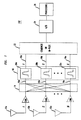
- FIG. 1 shows a general block diagram of a receiver according to the principles of the present invention;
- FIG. 2 shows the different frequency bands at the A/D input frequencies and the replicas of the analog signals in the different Nyquist zones which fold back to the first Nyquist zone in the digital domain;
- FIG. 3 shows a general block diagram of an example embodiment of a multiple band receiver according to principles of the present invention;
- FIG. 4 shows the frequency bands at the A/D input frequencies and the replicas of the frequency bands at the digital domain frequencies of the first Nyquist zone for the multiple band receiver of FIG. 3;
- FIG. 5 shows a Nyquist zone frequency plan for an A/D converter using a sampling rate of 61.44 MHz; and
- FIG. 6 shows Nyquist zone channels with replicas of the frequency bands at RF.
-
- Illustrative embodiments are described below of a receiver system using a single analog to digital (A/D) converter to convert RF analog signals into the digital domain. The RF analog signals are digitally converted using a sampling rate for the A/D converter which produces a replica of the signal bandwidth(s) at RF in the Nyquist bandwidth. As such, the receiver architecture according to the principles of the present invention does not require frequency conversion stage(s), which comprise mixer(s) and local oscillator(s), to down-convert the RF analog signals. Furthermore, by using a single A/D converter, the receiver provides time and/or phase coherent sampling of analog signals in different frequency band(s) in certain embodiments.
- With particular reference to FIG. 1, a
receiver 10 includesN antennas 12a-n which receive analog signals over RF communications channels, where N>=1. Theantenna 12a could be a multiple frequency band antenna. Achannel branch distributor 14, such as an N-plexer filter or combiner array, combines and/or separates the received RF analog signals or portions thereof and provides the received analog signals intoX channel branches 16a-x in a desired manner, where X>=1 and can but need not be equal to N. For example,different channel branches 16a-x can carry the analog signals for corresponding RF frequency bands, thechannel branches 16a-x can carry RF analog signals received by different antenna(s) or sets of antennas, and/or multiple channel branches having copies of the RF analog signals of different or contiguous frequency bands. In this embodiment, afilter arrangement 18 provides at least two different RF frequency bands on at least onechannel branch 16a-x. For example, thefilter arrangement 18 can include afilter 20a-x on eachchannel branch 16a-x which passes a frequency band on therespective channel branch 16a-x while attenuating other frequencies. Alternatively, depending on the embodiment, thechannel branch distributor 14 can simply include direct connection(s) from the antenna(s) 12a-n to thefilter arrangement 18, and thefilter arrangement 18 can include afilter 20a-x for eachchannel branch 16a-x. - A combining
arrangement 22 combines the RF analog signals on thechannel branches 16a-x in desired fashion. The resulting composite analog signal is provided with analog signals in different frequency bands to an analog todigital converter 24 which digitizes the RF analog signals and provides the digitized signals todigital processing circuitry 26. Alternatively, depending on the embodiment, if thereceiver 10 has asingle branch 16, the combiningarrangement 22 is simply a connection from theantenna 12 through the filter 20 (if required) to the A/D converter 24. - A sampling rate for the A/
D converter 24 is selected such that the frequency bands of the RF analog signals on thechannel branches 16a-x fold back to non-overlapping portions of the first Nyquist zone which reflects the Nyquist bandwidth provided by the analog to digital (A/D)converter 24. The Nyquist sampling rate for a modulated analog signal, for example where an information signal is modulated onto a carrier signal, can be defined as being at least twice the highest frequency component of the information signal regardless of the carrier frequency on which the information signal is modulated. The information, which can be voice, data, video, text and/or other information, is carried in the signal bandwidth. The highest frequency component of the information signal is directly related to the signal bandwidth. Because the signal bandwidth is sampled at at least twice the highest frequency component of the information signal, the information signal can be reproduced in the digital domain. - When the frequency spectrum is sampled by an A/
D converter 24 at the sampling rate of at least twice the combined signal bandwidth, which can be referred to as the Nyquist sampling rate, the signal bandwidth rotates or folds periodically about itself at frequency multiples or intervals ("Nyquist zones") of one-half the sampling frequency back to a first Nyquist zone in the digital domain from 0 Hz to one-half the sampling rate. As such, a signal bandwidth and a mirror image of the signal bandwidth periodically repeats at frequency intervals corresponding to the sampling rate of the A/D converter. For example, a signal bandwidth in an odd-numbered Nyquist zone will appear in the same relative position in odd numbered Nyquist zones back to the first Nyquist zone yet appear as a mirror image in the even-numbered Nyquist zones. Moreover, a signal bandwidth in an even-numbered Nyquist zone appears as a mirror image in the odd-numbered Nyquist zones back to the first Nyquist zone while appearing in the same relative position in the even-numbered Nyquist zones. Therefore, replicas of the signal bandwidth(s) are repeated at intervals of one-half the sampling rate. The sampling rate for the A/D converter is chosen such that after the analog signals are digitized, the desired replica frequency bands occupy non-overlapping portions or channels of the first Nyquist zone. The digital conversion effectively preserves the information being produced at a rate of less than or equal to one-half the sampling rate in the bandwidth of the first Nyquist zone. If the sampling rate is increased, the first Nyquist zone or Nyquist bandwidth becomes wider. - In this embodiment, a fast Fourier transform (FFT) of the digital signal values provides signals at frequency bands ("Nyquist zone channels") within one-half the sampling rate ("the first Nyquist zone") representing the converted analog signals. If the waveform is sampled at a rate less than twice its signal bandwidth (the Nyquist bandwidth), an undesirable overlapping between the adjacent periodic spectrums can occur - a well known phenomena known as aliasing. Accordingly, the sampling rate is chosen to avoid loss of information due to aliasing.
- For example, as shown in FIG. 2, in converting the analog signal at different RF bands into the digital domain, the A/
D converter 24 processes the composite analog signal intoNyquist zone channels 30a-x or bands in the first Nyquist zone. TheNyquist zone channels 30a-x in the digital domain correspond to thedifferent frequency bands 28a-x of the RF analog signals. The digitalsignal processing circuitry 26 can retrieve the digital signals from the Nyquist zone channels of the first Nyquist zone, because the different channels eventually end up in the first Nyquist zone after digitizing the analog input signals, for example using digital filters, digital combiners, digital detectors, digital demodulators, digital downconverters, such as a Digital Down Converter (DDC) with Numerical Controller Oscillator (NCO) to digitally down convert the data rate (which is referred to as decimation), and/or other digital processing. The DDC can tune to the respective frequencies for further signal processing. Therefore, thereceiver 10 can use the bandwidth available in a single A/D to process the RF analog signals from different RF frequency bands. - As such, the
receiver 10 according to the principles of the present invention eliminates the need for a mixer/LO combination on any of thechannel branches 16a-x. Areceiver 10 without a mixer/LO combination has many advantages. For example, without a fixed local oscillator (LO) in the frequency conversion stages, DC power consumption is reduced, re-radiation of LO out of the antenna is eliminated which reduces the need for extra front-end filtering, filter requirements at the IF are eliminated, and no image band filters are required. Because a mixer is not required, spurious mixer products as well as intermodulation distortion produced by the mixer are removed, thereby improving the spurious free dynamic range. Additionally, losses introduced by the mixer are removed which reduce the required channel gain and which improve the noise figure and the gain linearity. Furthermore, by using a single A/D converter, the receiver provides time and/or phase coherent sampling of analog signals in different frequency band(s). Different applications or signal processing schemes can benefit from such improved time and/or phase coherent measurements. - Depending on the embodiment and due to the flexibility of the receiver according to the principles of the present invention, the receiver can be implemented in different ways to use the potential bandwidth of an A/
D converter 24. FIG. 3 shows an embodiment of amultiple band receiver 50 according to certain principles of the present invention which is used to receive communications signals in the cellular and the Personal Communications System (PCS) frequency bands. In the United States, a base station for a "A" band cellular service provider receives frequency channels within the A (825-835MHz), A" (824-825MHz) and A' (845-846.5 MHz) bands. A base station for a B band cellular service provider uses the B (835-845MHz) and B' (846.5-849MHz) frequency bands. In this example, afirst antenna 12a receives the modulated analog signals within the entire cellular base station receive band (824-849 MHz), and asecond antenna 12b receives the modulated analog signals in the entire PCS base station receive band (1850-1910 MHz). - In this embodiment, the RF analog signals from the
antenna 12a are provided to afirst channel branch 16a, and the RF analog signals from theantenna 12b are provided to asecond channel branch 16b. Abandpass filter 20a on thefirst channel branch 16a passes the frequencies in the cellular band (824-849 MHz) and attenuates all other frequencies. Abandpass filter 20b on thesecond channel branch 16b passes the frequencies in the PCS band (1850-1910 MHz) and attenuates all other frequencies. In this embodiment, low noise amplifiers (LNAs) 52a-b amplify the analog signals on therespective channel branches 16a-b. A combiningarrangement 56 receives the analog signals on the first andsecond channel branches 16a-b and provides the combined analog signals of the two different frequency bands to the A/D converter 24. The combiningarrangement 56 can be a power combiner or a multiplexer filter. - In this example, the total bandwidth of the RF analog signals on the
different branches 16a-b is 85 MHz after adding the cellular (25 MHz) and the PCS (60MHz) bands. As such, a sampling rate for the A/D converter 24 is used such that the Nyquist bandwidth is sufficient to handle the 85 MHz bandwidth of the RF analog signals. Additionally, the sampling rate for the A/D converter 24 is selected such that the different frequency bands are replicated in non-overlapping portions of the Nyquist bandwidth. As such, the relative positioning of the different frequency bands within the respective Nyquist zone effects the choice of the sampling rate. For illustrative purposes, a 400MHz sampling rate (400 Mega Samples per second) is used for the A/D converter 24 to provide a Nyquist zone bandwidth of 200 MHz (one-half the sampling rate). In practice, a different sampling rate may be selected to provide a different bandwidth or guard bands between the signals of the different frequency bands or branches. The A/D converter 24 samples the combined or composite analog signals in the cellular band (824-849 MHz) and in the PCS band (1850-1910 MHz). In doing so, the A/D converter 24 produces for thedigital processing circuitry 26 converted signals in a Nyquist zone channel at 24-49 MHz corresponding to the signal bandwidth in the cellular band and converted signals in a Nyquist zone channel at 90-150 MHz corresponding to the signal bandwidth in the PCS band. - FIG. 4 shows the frequency spectrum produced by the A/
D converter 24 whereNyquist zones 60a-j are repeated across the frequency spectrum at intervals of the Nyquist bandwidth or 200MHz. The cellular band appears in the fifth Nyquist zone 60e at the A/D input frequencies of 824 -849 MHz which are the RF frequencies. A replica of the cellular band appears in each of the Nyquist zones back to thefirst Nyquist zone 60a which provides recovery of the information signal of the cellular band at a Nyquist zone channel between 24 and 49 MHz. The PCS band appears in thetenth Nyquist zone 60j at the A/D input frequencies of 1850 -1910 MHz which are the RF frequencies. A replica of the PCS band appears in each of the Nyquist zones back to thefirst Nyquist zone 60a which provides recovery of the information signal of the PCS band at a Nyquist zone channel between 90 and 150 MHz corresponding to a mirror image of the 1850-1910 MHz A/D input frequencies. - By properly selecting the sampling rate for the A/
D converter 24, the receiver according to the principles of the present invention can increase the utilization of the potential Nyquist bandwidth provided by the A/D converter 24 to receive RF analog signals in different frequency bands separated by large frequency differences. In the above example, the entire cellular and PCS bands were received and digitally converted using a single A/D converter using a sampling rate of 400 MHz. In sampling the analog signals at the RF frequencies, the A/D converter provides replicas or images of the RF frequency bands in the first Nyquist zone which are available for digital signal processing. In other embodiments, different sampling rates can be used to increase or decrease the Nyquist bandwidth, for example to provide extra bandwidth or guard bands between the signals of the different frequency bands. - For example, FIG. 5 shows a Nyquist zone frequency plan for an A/D converter using a sampling rate of 61.44 MHz which provides Nyquist zones which are 30.72 MHz wide. The Nyquist zones are shown as 15 MHz bandwidths within each Nyquist zone as being in-band. FIG. 6 shows a first Nyquist zone that is 30.72 MHz wide in which replicas of signals in different frequency bands at higher Nyquist zones are shown in non-overlapping portions or channels of the first Nyquist zone. A first
Nyquist zone channel 80 is shown at about 7.5 MHz with a replica of an amplitude modulated (AM) analog signal folded back fromNyquist zone 12 at 361 MHz with a 400 kHz bandwidth. A secondNyquist zone channel 82 is shown about 10 MHz with a replica of a code division multiple access (CDMA) signal folded back fromNyquist zone 61 at 1853 MHz with a 2MHz bandwidth. A thirdNyquist zone channel 84 is shown at about 18.75 MHz with a replica of a continuous wave (CW) single tone signal folded back fromNyquist zone 5 at 141.7 MHz. Finally, a fourthNyquist zone channel 86 is shown at about 22MHz with a replica of a frequency modulated (FM) signal folded back fromNyquist zone 17 at 513.5 MHz with a 4 MHz bandwidth. Accordingly, the receiver according to the principles of the present invention can receive and digitally convert analog signals from systems using different, the same or no multiple access techniques, using the same and/or different modulation techniques, and/or using different and/or contiguous frequency bands or schemes in a single A/D converter without frequency conversion of the RF frequency bands. The analog signals can be characterized as wideband, broadband and/or narrowband. - In addition to the embodiment described above, alternative configurations of the receiver architecture according to the principles of the present invention are possible which omit and/or add components and/or use variations or portions of the described receiver architecture. For example, with particular reference to FIG. 3, an AM broadcast radio frequency band (550-1600 kHz) can be received by an
antenna 76 and added to the combined or composite analog signal, and the A/D converter 24 could digitize the analog signals in the AM radio frequency band. The AM radio frequency band would be located in the kilohertz range of the first Nyquist zone. As such, the receiver according to the principles of the present invention could receive signals from different sources, such as the base stations for cellular or PCS systems, AM or FM broadcast radio stations and/or GPS satellites. As would be understood by one of ordinary skill in the art, the various components making up the receiver architecture and their respective operating parameters and characteristics should be properly matched up to provide the proper operation. For example, an embodiment of the receiver system can be used to receive signals from a North American TDMA system, a Global System For Mobile Communication (GSM) system, a code division multiple access (CDMA) system, frequency division multiple access (FDMA) systems, Global Positioning System (GPS), FM radio and/or AM radio. Additionally, the embodiments of the receiver according to the principles of the present invention have been described with frequency band(s) associated with base station receive frequencies, but the receiver architecture according to the principles of the present invention can be used in wireless units, such as mobile units, receiving information from other frequency band(s), such as a base station transmit band which is a mobile unit receive band. - Furthermore, the receiver system has been described using particular configurations of distinct components, but it should be understood that the receiver system and portions thereof can be implemented in application specific integrated circuits, software-driven processing circuitry, firmware, programmable logic devices, hardware or other arrangements of discrete components as would be understood by one of ordinary skill in the art with the benefit of this disclosure. Although in the illustrative embodiment is shown with a particular circuitry, the measurement radio architecture can use different components which together perform similar functions when compared to the circuitry shown. What has been described is merely illustrative of the application of the principles of the present invention. Those skilled in the art will readily recognize that these and various other modifications, arrangements and methods can be made to the present invention without strictly following the exemplary applications illustrated and described herein and without departing from the spirit and scope of the present invention.
Claims (12)
- A method of processing received signals, said method CHARACTERIZED BY:providing analog signals at radio frequency (RF); anddigitally converting said analog signals at RF.
- The method of claim 1 CHARACTERIZED BY:providing analog signals at different RF frequency bands; anddigitally converting said analog signals at said different RF frequency bands.
- The method of claim 1 CHARACTERIZED BY:providing analog signals on a plurality of channel branches (16a-b) at radio frequency (RF);combining said RF analog signals on said plurality of channel branches (16a-b) at RF; anddigitally converting said composite analog signals at RF.
- The method of claim 1 CHARACTERIZED BY:
receiving said analog signals on at least two antennas (12a-b). - The method of claim 4 CHARACTERIZED IN THAT said providing including:using a first antenna (12a) to provide analog signals of a frequency band on a first channel branch (16a); andusing a second antenna (12b) to provide analog signals of a second frequency band on a second channel branch (16b).
- The method of claim 3 CHARACTERIZED IN THAT said providing further including:
filtering on each channel branch (16a-b) said analog signals to provide analog signals having a frequency band corresponding to said channel branch. - The method of claim 3 CHARACTERIZED IN THAT said providing further including:receiving analog signals from at least one antenna (12a); andselectively producing on each channel branch (16a-b) analog signals having a frequency band corresponding to said channel branch (16a-b).
- A receiver (10) CHARACTERIZED BY:at least one antenna (12a) for receiving and providing analog signals at radio frequencies (RF); andan analog to digital converter (24) configured to receive and digitally convert said received analog signals at RF.
- The receiver of claim 8 CHARACTERIZED BY:at least one antenna (12a) for receiving analog signals in different radio frequency (RF) bands; andan analog to digital converter (24) configured to receive and digitally convert said analog signals at different RF bands.
- The receiver of claim 8 CHARACTERIZED BY:a channel branch arranger (14) connected to said at least one antenna (12a) for receiving analog signals and providing analog signals onto a plurality of channel branches (16a-b) at radio frequencies (RF);a combining arrangement (22) connected to said plurality of channel branches (16a-b) to combine said analog signals on said plurality of channel branches (16a-b); andan analog to digital converter configured to receive and digitally convert said combined analog signals at RF.
- The receiver of claim 10 CHARACTERIZED BY:
at least two antennas (12a-b) to provide said channel branch arranger (14) with said analog signals. - The receiver of claim 11 CHARACTERIZED IN THAT said channel branch arranger (14) configured to provide on a first channel branch (16a) analog signals from a first antenna of a frequency band and to provide on a second channel branch (16b) analog signals from a second antenna (12b) of a second frequency band.
Applications Claiming Priority (2)
| Application Number | Priority Date | Filing Date | Title |
|---|---|---|---|
| US548995 | 2000-04-14 | ||
| US09/548,995 US6678512B1 (en) | 2000-04-14 | 2000-04-14 | Receiver system using analog to digital conversion at radio frequency and method |
Publications (2)
| Publication Number | Publication Date |
|---|---|
| EP1148653A1 true EP1148653A1 (en) | 2001-10-24 |
| EP1148653B1 EP1148653B1 (en) | 2002-09-25 |
Family
ID=24191226
Family Applications (1)
| Application Number | Title | Priority Date | Filing Date |
|---|---|---|---|
| EP00309813A Expired - Lifetime EP1148653B1 (en) | 2000-04-14 | 2000-11-06 | Receiver system using analog to digital conversion at radio frequency and method |
Country Status (9)
| Country | Link |
|---|---|
| US (1) | US6678512B1 (en) |
| EP (1) | EP1148653B1 (en) |
| JP (1) | JP3614790B2 (en) |
| KR (1) | KR100539846B1 (en) |
| CN (1) | CN1318957A (en) |
| AU (1) | AU3508201A (en) |
| BR (1) | BRPI0101297B1 (en) |
| CA (1) | CA2337714C (en) |
| DE (1) | DE60000503T2 (en) |
Cited By (6)
| Publication number | Priority date | Publication date | Assignee | Title |
|---|---|---|---|---|
| EP1839396A2 (en) * | 2005-01-13 | 2007-10-03 | Nxp B.V. | Low intermediate frequency receiver and the sampling method thereof |
| EP1842355A4 (en) * | 2005-01-20 | 2009-11-11 | Skyworks Solutions Inc | INTEGRATED MULTIBAND EMITTER-RECEIVER FOR USE IN A MOBILE COMMUNICATION DEVICE |
| WO2011038484A1 (en) | 2009-09-30 | 2011-04-07 | Wi-Lan, Inc. | Radio frequency front end and spectrum sensor |
| EP2245741A4 (en) * | 2008-01-16 | 2011-08-03 | Lockheed Corp | Direct rf complex analog to digital converter |
| US8976302B2 (en) | 2009-09-30 | 2015-03-10 | Wi-Lan, Inc. | Radio frequency front end for television band receiver and spectrum sensor |
| US9130609B2 (en) | 2010-10-19 | 2015-09-08 | Commscope Technologies Llc | Systems and methods for transporting digital RF signals |
Families Citing this family (49)
| Publication number | Priority date | Publication date | Assignee | Title |
|---|---|---|---|---|
| US6895310B1 (en) * | 2000-04-24 | 2005-05-17 | Usa Technologies, Inc. | Vehicle related wireless scientific instrumentation telematics |
| US6856820B1 (en) * | 2000-04-24 | 2005-02-15 | Usa Technologies, Inc. | In-vehicle device for wirelessly connecting a vehicle to the internet and for transacting e-commerce and e-business |
| US7502672B1 (en) | 2000-04-24 | 2009-03-10 | Usa Technologies, Inc. | Wireless vehicle diagnostics with service and part determination capabilities |
| US6859652B2 (en) * | 2000-08-02 | 2005-02-22 | Mobile Satellite Ventures, Lp | Integrated or autonomous system and method of satellite-terrestrial frequency reuse using signal attenuation and/or blockage, dynamic assignment of frequencies and/or hysteresis |
| US20020193090A1 (en) * | 2001-05-23 | 2002-12-19 | Sugar Gary L. | System and method for dynamic sampling rate adjustment to minimize power consumption in wideband radios |
| US6865376B2 (en) * | 2001-07-03 | 2005-03-08 | Kyocera Wireless Corp. | System and method for a GPS enabled antenna |
| JP2003318732A (en) * | 2002-04-26 | 2003-11-07 | Hitachi Ltd | Communication semiconductor integrated circuit and wireless communication system |
| US7570189B2 (en) * | 2002-06-27 | 2009-08-04 | Nxp B.V. | Radio frequency data capture |
| DE10315408A1 (en) * | 2003-04-04 | 2004-10-14 | Robert Bosch Gmbh | Receiving unit and method for receiving an analog received signal |
| US7376440B2 (en) * | 2003-04-16 | 2008-05-20 | Kyocera Wireless Corp. | N-plexer systems and methods for use in a wireless communications device |
| US20060227898A1 (en) * | 2003-07-10 | 2006-10-12 | Gibson Timothy P | Radio receiver |
| US7382840B2 (en) * | 2003-07-29 | 2008-06-03 | Mitsubishi Electric Research Laboratories, Inc. | RF signal processing in multi-antenna systems |
| US7522901B2 (en) * | 2004-01-20 | 2009-04-21 | Broadcom Corporation | Direct digital conversion tuner and method for using same |
| US8000675B2 (en) * | 2004-04-16 | 2011-08-16 | Sony Ericsson Mobile Communications Ab | Low cost method for receiving broadcast channels with a cellular terminal |
| US7400904B2 (en) * | 2004-12-03 | 2008-07-15 | Itron, Inc. | Dual mode AM-FM receiver with I-Q decoding, such as for utility data collection |
| CN2749181Y (en) * | 2004-12-28 | 2005-12-28 | 精恒科技集团有限公司 | Multi-antenna receiving and output processing device |
| US7274326B2 (en) * | 2005-02-24 | 2007-09-25 | Honeywell International Inc. | System for digital multi-bandwidth intermediate frequency processing and tracking |
| DE602006007071D1 (en) * | 2005-09-16 | 2009-07-16 | Toshiba Kk | Analog signal processing circuit and communication device with it |
| KR100983547B1 (en) * | 2005-11-21 | 2010-09-24 | 후지쓰 텐 가부시키가이샤 | Receiver apparatus |
| JP4662480B2 (en) * | 2006-06-10 | 2011-03-30 | Kddi株式会社 | Method and program for determining sampling frequency in undersampling |
| US20080084861A1 (en) * | 2006-10-10 | 2008-04-10 | Honeywell International Inc. | Avionics communication system and method utilizing multi-channel radio technology and a shared data bus |
| EP1978647A3 (en) * | 2007-04-05 | 2013-10-09 | Delphi Delco Electronics Europe GmbH | Broadband receiver system |
| EP2143214A2 (en) * | 2007-05-10 | 2010-01-13 | Astrium Limited | Signal processing system |
| US8081933B2 (en) * | 2007-07-13 | 2011-12-20 | Honeywell International Inc. | Reconfigurable aircraft radio communications system |
| US20090258640A1 (en) * | 2008-04-11 | 2009-10-15 | Telefonaktiebolaget Lm Ericsson | Device power detector |
| US8019338B2 (en) * | 2008-05-29 | 2011-09-13 | Honeywell International Inc. | Reconfigurable aircraft communications system with integrated avionics communication router and audio management functions |
| US8289811B2 (en) * | 2009-09-01 | 2012-10-16 | The Johns Hopkins University | System and method for determining location of submerged submersible vehicle |
| CN101729081A (en) * | 2008-10-17 | 2010-06-09 | 鸿富锦精密工业(深圳)有限公司 | Dual-frequency-band receiving system and electronic device applying same |
| WO2010050960A1 (en) * | 2008-10-30 | 2010-05-06 | Hewlett-Packard Development Company, L.P. | Wireless device with selectable antennas |
| US8509368B2 (en) * | 2008-12-18 | 2013-08-13 | L-3 Communications Integrated Systems, L.P. | System and method for clock jitter compensation in direct RF receiver architectures |
| DE102009028919A1 (en) * | 2009-08-27 | 2011-03-03 | Robert Bosch Gmbh | Method and controller for direct sampling of a plurality of radio bands |
| AU2011207101B2 (en) * | 2010-01-19 | 2014-07-17 | Advanced Micro Devices, Inc. | Estimation of signal to noise ratio in receivers |
| CN102377432B (en) * | 2010-08-27 | 2015-01-07 | 国民技术股份有限公司 | Multiplex analog-to-digital conversion device |
| US8711993B2 (en) | 2010-12-10 | 2014-04-29 | Honeywell International Inc. | Wideband multi-channel receiver with fixed-frequency notch filter for interference rejection |
| US9184771B2 (en) * | 2011-10-12 | 2015-11-10 | Optis Cellular Technology, Llc | Digital down conversion and demodulation |
| CN103580719A (en) * | 2012-08-06 | 2014-02-12 | 上海航天测控通信研究所 | Full-digital intermediate-frequency despreading demodulation receiver |
| US9614629B2 (en) * | 2012-08-15 | 2017-04-04 | Commscope Technologies Llc | Telecommunication system using multiple Nyquist zone operations |
| WO2014036984A1 (en) | 2012-09-06 | 2014-03-13 | Eads Deutschland Gmbh | Radar receiver and method for receiving receive signals in a radar receiver |
| CN103684492A (en) * | 2012-09-24 | 2014-03-26 | 中兴通讯股份有限公司 | Radio frequency signal sampling device, a reception machine and a base station. |
| US10277346B1 (en) * | 2015-07-10 | 2019-04-30 | The United States Of America As Represented By The Administrator Of National Aeronautics And Space Administration | High-efficiency secondary signal combiner |
| US10069568B1 (en) | 2017-03-02 | 2018-09-04 | Harris Corporation | Communications system providing photonic conversion and power detection and related methods |
| JP2018174415A (en) * | 2017-03-31 | 2018-11-08 | 国立大学法人東北大学 | Multiband reception apparatus and reception method of multiband high-frequency signal |
| IL261857B (en) * | 2018-09-17 | 2020-02-27 | Elbit System Bmd And Land Ew Elisra Ltd | Systems and method for reducing spurious signals in a |
| JP2020072411A (en) * | 2018-10-31 | 2020-05-07 | アイコム株式会社 | AD converter and electronic device |
| US11251832B2 (en) | 2020-03-02 | 2022-02-15 | L-3 Communications Integrated Systems L.P. | Multiple clock sampling for Nyquist folded sampling receivers |
| US11038728B1 (en) * | 2020-10-01 | 2021-06-15 | Honeywell International Inc. | Demodulating surveillance signals |
| US11258469B1 (en) | 2020-10-01 | 2022-02-22 | Honeywell International Inc. | Demodulating surveillance signals |
| US11356309B2 (en) | 2020-10-01 | 2022-06-07 | Honeywell International Inc. | Demodulating surveillance signals |
| US12665605B1 (en) | 2024-11-07 | 2026-06-23 | Bae Systems Information And Electronic Systems Integration Inc. | Hybrid wideband / narrowband direct digital transceiver |
Citations (2)
| Publication number | Priority date | Publication date | Assignee | Title |
|---|---|---|---|---|
| US5602847A (en) * | 1995-09-27 | 1997-02-11 | Lucent Technologies Inc. | Segregated spectrum RF downconverter for digitization systems |
| GB2338853A (en) * | 1998-06-18 | 1999-12-29 | Ericsson Telefon Ab L M | Double band superheterodyne receiver with single A/D converter |
Family Cites Families (6)
| Publication number | Priority date | Publication date | Assignee | Title |
|---|---|---|---|---|
| US5995556A (en) * | 1990-06-06 | 1999-11-30 | California Institute Of Technology | Front end for GPS receivers |
| US5280636A (en) * | 1991-06-13 | 1994-01-18 | Hughes Aircraft Company | Multi-band digital receiving apparatus and method with bandwidth reduction |
| FI97838C (en) * | 1992-05-06 | 1997-02-25 | Nokia Telecommunications Oy | Cellulärnätsystem |
| US5697078A (en) * | 1994-03-25 | 1997-12-09 | Steinbrecher Corporation | Wideband channel sniffer for monitoring channel use in a wireless communication system |
| WO1997005705A1 (en) | 1995-07-26 | 1997-02-13 | Telefonaktiebolaget Lm Ericsson (Publ) | Amps a-band single superhet |
| JPH11127085A (en) * | 1997-10-20 | 1999-05-11 | Fujitsu Ltd | Two-mode demodulator |
-
2000
- 2000-04-14 US US09/548,995 patent/US6678512B1/en not_active Expired - Lifetime
- 2000-11-06 DE DE60000503T patent/DE60000503T2/en not_active Expired - Lifetime
- 2000-11-06 EP EP00309813A patent/EP1148653B1/en not_active Expired - Lifetime
-
2001
- 2001-02-22 CA CA002337714A patent/CA2337714C/en not_active Expired - Lifetime
- 2001-04-03 BR BRPI0101297A patent/BRPI0101297B1/en not_active IP Right Cessation
- 2001-04-10 AU AU35082/01A patent/AU3508201A/en not_active Abandoned
- 2001-04-11 CN CN01116523A patent/CN1318957A/en active Pending
- 2001-04-13 KR KR10-2001-0019758A patent/KR100539846B1/en not_active Expired - Lifetime
- 2001-04-13 JP JP2001114703A patent/JP3614790B2/en not_active Expired - Lifetime
Patent Citations (2)
| Publication number | Priority date | Publication date | Assignee | Title |
|---|---|---|---|---|
| US5602847A (en) * | 1995-09-27 | 1997-02-11 | Lucent Technologies Inc. | Segregated spectrum RF downconverter for digitization systems |
| GB2338853A (en) * | 1998-06-18 | 1999-12-29 | Ericsson Telefon Ab L M | Double band superheterodyne receiver with single A/D converter |
Non-Patent Citations (1)
| Title |
|---|
| LAWTON M C ET AL: "THE DESIGN OF FLEXIBLE RECEIVERS FOR COMMUNICATING APPLIANCES", MOBILE TECHNOLOGY FOR THE HUMAN RACE. ATLANTA, APR. 28 - MAY 1, 1996,NEW YORK, IEEE,US, vol. CONF. 46, 28 April 1996 (1996-04-28), pages 1060 - 1064, XP000593125, ISBN: 0-7803-3158-3 * |
Cited By (11)
| Publication number | Priority date | Publication date | Assignee | Title |
|---|---|---|---|---|
| EP1839396A2 (en) * | 2005-01-13 | 2007-10-03 | Nxp B.V. | Low intermediate frequency receiver and the sampling method thereof |
| EP1842355A4 (en) * | 2005-01-20 | 2009-11-11 | Skyworks Solutions Inc | INTEGRATED MULTIBAND EMITTER-RECEIVER FOR USE IN A MOBILE COMMUNICATION DEVICE |
| EP2245741A4 (en) * | 2008-01-16 | 2011-08-03 | Lockheed Corp | Direct rf complex analog to digital converter |
| WO2011038484A1 (en) | 2009-09-30 | 2011-04-07 | Wi-Lan, Inc. | Radio frequency front end and spectrum sensor |
| EP2484108A4 (en) * | 2009-09-30 | 2014-01-22 | Wi Lan Inc | Radio frequency front end and spectrum sensor |
| US8976302B2 (en) | 2009-09-30 | 2015-03-10 | Wi-Lan, Inc. | Radio frequency front end for television band receiver and spectrum sensor |
| US9130609B2 (en) | 2010-10-19 | 2015-09-08 | Commscope Technologies Llc | Systems and methods for transporting digital RF signals |
| US9450653B2 (en) | 2010-10-19 | 2016-09-20 | Commscope Technologies Llc | Systems and methods for transporting digital RF signals |
| US9755868B2 (en) | 2010-10-19 | 2017-09-05 | Commscope Technologies Llc | Systems and methods for transporting digital RF signals |
| US10110403B2 (en) | 2010-10-19 | 2018-10-23 | Commscope Technologies Llc | Systems and methods for transporting digital RF signals |
| US10432437B2 (en) | 2010-10-19 | 2019-10-01 | Commscope Technologies Llc | Systems and methods for transporting digital RF signals |
Also Published As
| Publication number | Publication date |
|---|---|
| BRPI0101297B1 (en) | 2015-12-29 |
| DE60000503D1 (en) | 2002-10-31 |
| CA2337714A1 (en) | 2001-10-14 |
| CA2337714C (en) | 2005-09-13 |
| AU3508201A (en) | 2001-10-18 |
| BR0101297A (en) | 2001-11-13 |
| DE60000503T2 (en) | 2003-06-26 |
| CN1318957A (en) | 2001-10-24 |
| US6678512B1 (en) | 2004-01-13 |
| KR20010098566A (en) | 2001-11-08 |
| KR100539846B1 (en) | 2005-12-28 |
| JP2002026758A (en) | 2002-01-25 |
| EP1148653B1 (en) | 2002-09-25 |
| JP3614790B2 (en) | 2005-01-26 |
Similar Documents
| Publication | Publication Date | Title |
|---|---|---|
| CA2337714C (en) | Receiver system using analog to digital conversion at radio frequency and method | |
| EP1154589B1 (en) | Multiple branch receiver system and method | |
| US5602847A (en) | Segregated spectrum RF downconverter for digitization systems | |
| KR100829766B1 (en) | Multipath communication receiver | |
| FI114177B (en) | Digitizer and digitization method for broadband signal | |
| KR0149893B1 (en) | Method and apparatus for receiving electromagnetic radiation within a frequency band | |
| US20070066254A1 (en) | Analog signal processing circuit and communication device therewith | |
| KR20050096208A (en) | System and method for a direct conversion multi-carrier processor | |
| JP2002518878A (en) | Apparatus and method for digital channel separation and channel integration | |
| CN107147427A (en) | A kind of method of sampling of signal, device and system | |
| CN102082578B (en) | General ultra-wideband reception method | |
| CN101174840A (en) | Programmable direct RF digital receiver with multiple frequency bands and method thereof | |
| Tseng et al. | Direct downconversion of multiple RF signals using bandpass sampling | |
| Im et al. | Implementation of SDR-based digital IF channelizer/de-channelizer for multiple CDMA signals | |
| JP4018406B2 (en) | Method and transmitter for processing digital signals in analog form | |
| EP2403145A1 (en) | A receiver and a method for processing a signal | |
| RU2555862C2 (en) | Method for direct signal sampling of multiple radio frequency bands and control unit therefor | |
| KR100964383B1 (en) | Digital Intensive RF Receiver | |
| Efstathiou | Base station transceiver trends for 3G and beyond wireless systems |
Legal Events
| Date | Code | Title | Description |
|---|---|---|---|
| PUAI | Public reference made under article 153(3) epc to a published international application that has entered the european phase |
Free format text: ORIGINAL CODE: 0009012 |
|
| 17P | Request for examination filed |
Effective date: 20001117 |
|
| AK | Designated contracting states |
Kind code of ref document: A1 Designated state(s): DE FI FR GB SE Kind code of ref document: A1 Designated state(s): AT BE CH CY DE DK ES FI FR GB GR IE IT LI LU MC NL PT SE TR |
|
| AX | Request for extension of the european patent |
Free format text: AL;LT;LV;MK;RO;SI |
|
| 17Q | First examination report despatched |
Effective date: 20010625 |
|
| GRAG | Despatch of communication of intention to grant |
Free format text: ORIGINAL CODE: EPIDOS AGRA |
|
| GRAG | Despatch of communication of intention to grant |
Free format text: ORIGINAL CODE: EPIDOS AGRA |
|
| GRAH | Despatch of communication of intention to grant a patent |
Free format text: ORIGINAL CODE: EPIDOS IGRA |
|
| GRAH | Despatch of communication of intention to grant a patent |
Free format text: ORIGINAL CODE: EPIDOS IGRA |
|
| AKX | Designation fees paid |
Free format text: DE FI FR GB SE |
|
| GRAA | (expected) grant |
Free format text: ORIGINAL CODE: 0009210 |
|
| AK | Designated contracting states |
Kind code of ref document: B1 Designated state(s): DE FI FR GB SE |
|
| REG | Reference to a national code |
Ref country code: GB Ref legal event code: FG4D |
|
| REF | Corresponds to: |
Ref document number: 60000503 Country of ref document: DE Date of ref document: 20021031 |
|
| PG25 | Lapsed in a contracting state [announced via postgrant information from national office to epo] |
Ref country code: SE Free format text: LAPSE BECAUSE OF NON-PAYMENT OF DUE FEES Effective date: 20021107 |
|
| ET | Fr: translation filed | ||
| EUG | Se: european patent has lapsed | ||
| PLBE | No opposition filed within time limit |
Free format text: ORIGINAL CODE: 0009261 |
|
| STAA | Information on the status of an ep patent application or granted ep patent |
Free format text: STATUS: NO OPPOSITION FILED WITHIN TIME LIMIT |
|
| 26N | No opposition filed |
Effective date: 20030626 |
|
| REG | Reference to a national code |
Ref country code: GB Ref legal event code: 732E Free format text: REGISTERED BETWEEN 20131031 AND 20131106 |
|
| REG | Reference to a national code |
Ref country code: FR Ref legal event code: CD Owner name: ALCATEL-LUCENT USA INC. Effective date: 20131122 |
|
| REG | Reference to a national code |
Ref country code: FR Ref legal event code: GC Effective date: 20140410 |
|
| REG | Reference to a national code |
Ref country code: FR Ref legal event code: RG Effective date: 20141015 |
|
| REG | Reference to a national code |
Ref country code: FR Ref legal event code: PLFP Year of fee payment: 16 |
|
| REG | Reference to a national code |
Ref country code: FR Ref legal event code: PLFP Year of fee payment: 17 |
|
| REG | Reference to a national code |
Ref country code: FR Ref legal event code: PLFP Year of fee payment: 18 |
|
| REG | Reference to a national code |
Ref country code: FR Ref legal event code: PLFP Year of fee payment: 19 |
|
| PGFP | Annual fee paid to national office [announced via postgrant information from national office to epo] |
Ref country code: DE Payment date: 20191022 Year of fee payment: 20 Ref country code: FI Payment date: 20191111 Year of fee payment: 20 |
|
| PGFP | Annual fee paid to national office [announced via postgrant information from national office to epo] |
Ref country code: FR Payment date: 20191014 Year of fee payment: 20 |
|
| PGFP | Annual fee paid to national office [announced via postgrant information from national office to epo] |
Ref country code: GB Payment date: 20191108 Year of fee payment: 20 |
|
| REG | Reference to a national code |
Ref country code: DE Ref legal event code: R071 Ref document number: 60000503 Country of ref document: DE |
|
| REG | Reference to a national code |
Ref country code: GB Ref legal event code: PE20 Expiry date: 20201105 |
|
| REG | Reference to a national code |
Ref country code: FI Ref legal event code: MAE |
|
| PG25 | Lapsed in a contracting state [announced via postgrant information from national office to epo] |
Ref country code: GB Free format text: LAPSE BECAUSE OF EXPIRATION OF PROTECTION Effective date: 20201105 |