EP1148629A2 - Steuerverfahren für einen pulsweitengesteuerten Umrichter und Steuervorrichtung zur Durchführung dieses Steuerverfahrens - Google Patents
Steuerverfahren für einen pulsweitengesteuerten Umrichter und Steuervorrichtung zur Durchführung dieses Steuerverfahrens Download PDFInfo
- Publication number
- EP1148629A2 EP1148629A2 EP01106236A EP01106236A EP1148629A2 EP 1148629 A2 EP1148629 A2 EP 1148629A2 EP 01106236 A EP01106236 A EP 01106236A EP 01106236 A EP01106236 A EP 01106236A EP 1148629 A2 EP1148629 A2 EP 1148629A2
- Authority
- EP
- European Patent Office
- Prior art keywords
- voltage system
- soll
- voltage
- zero
- angle
- Prior art date
- Legal status (The legal status is an assumption and is not a legal conclusion. Google has not performed a legal analysis and makes no representation as to the accuracy of the status listed.)
- Granted
Links
- 238000000034 method Methods 0.000 title claims description 46
- 239000004065 semiconductor Substances 0.000 claims abstract description 21
- 230000006870 function Effects 0.000 claims description 50
- 230000007704 transition Effects 0.000 claims description 13
- 241001270131 Agaricus moelleri Species 0.000 description 24
- 230000008901 benefit Effects 0.000 description 14
- 230000008859 change Effects 0.000 description 10
- 230000008569 process Effects 0.000 description 8
- 230000009467 reduction Effects 0.000 description 6
- 230000006399 behavior Effects 0.000 description 4
- 238000005336 cracking Methods 0.000 description 3
- 230000000630 rising effect Effects 0.000 description 3
- 238000006073 displacement reaction Methods 0.000 description 2
- 230000015572 biosynthetic process Effects 0.000 description 1
- 230000001419 dependent effect Effects 0.000 description 1
- 238000010586 diagram Methods 0.000 description 1
- 230000000694 effects Effects 0.000 description 1
- 230000010363 phase shift Effects 0.000 description 1
- 238000005070 sampling Methods 0.000 description 1
- 230000001629 suppression Effects 0.000 description 1
- 230000002123 temporal effect Effects 0.000 description 1
Images


Classifications
-
- H—ELECTRICITY
- H02—GENERATION; CONVERSION OR DISTRIBUTION OF ELECTRIC POWER
- H02M—APPARATUS FOR CONVERSION BETWEEN AC AND AC, BETWEEN AC AND DC, OR BETWEEN DC AND DC, AND FOR USE WITH MAINS OR SIMILAR POWER SUPPLY SYSTEMS; CONVERSION OF DC OR AC INPUT POWER INTO SURGE OUTPUT POWER; CONTROL OR REGULATION THEREOF
- H02M7/00—Conversion of AC power input into DC power output; Conversion of DC power input into AC power output
- H02M7/42—Conversion of DC power input into AC power output without possibility of reversal
- H02M7/44—Conversion of DC power input into AC power output without possibility of reversal by static converters
- H02M7/48—Conversion of DC power input into AC power output without possibility of reversal by static converters using discharge tubes with control electrode or semiconductor devices with control electrode
- H02M7/505—Conversion of DC power input into AC power output without possibility of reversal by static converters using discharge tubes with control electrode or semiconductor devices with control electrode using devices of a thyratron or thyristor type requiring extinguishing means
- H02M7/515—Conversion of DC power input into AC power output without possibility of reversal by static converters using discharge tubes with control electrode or semiconductor devices with control electrode using devices of a thyratron or thyristor type requiring extinguishing means using semiconductor devices only
- H02M7/525—Conversion of DC power input into AC power output without possibility of reversal by static converters using discharge tubes with control electrode or semiconductor devices with control electrode using devices of a thyratron or thyristor type requiring extinguishing means using semiconductor devices only with automatic control of output waveform or frequency
- H02M7/527—Conversion of DC power input into AC power output without possibility of reversal by static converters using discharge tubes with control electrode or semiconductor devices with control electrode using devices of a thyratron or thyristor type requiring extinguishing means using semiconductor devices only with automatic control of output waveform or frequency by pulse width modulation
-
- H—ELECTRICITY
- H02—GENERATION; CONVERSION OR DISTRIBUTION OF ELECTRIC POWER
- H02M—APPARATUS FOR CONVERSION BETWEEN AC AND AC, BETWEEN AC AND DC, OR BETWEEN DC AND DC, AND FOR USE WITH MAINS OR SIMILAR POWER SUPPLY SYSTEMS; CONVERSION OF DC OR AC INPUT POWER INTO SURGE OUTPUT POWER; CONTROL OR REGULATION THEREOF
- H02M1/00—Details of apparatus for conversion
- H02M1/0048—Circuits or arrangements for reducing losses
-
- H—ELECTRICITY
- H02—GENERATION; CONVERSION OR DISTRIBUTION OF ELECTRIC POWER
- H02M—APPARATUS FOR CONVERSION BETWEEN AC AND AC, BETWEEN AC AND DC, OR BETWEEN DC AND DC, AND FOR USE WITH MAINS OR SIMILAR POWER SUPPLY SYSTEMS; CONVERSION OF DC OR AC INPUT POWER INTO SURGE OUTPUT POWER; CONTROL OR REGULATION THEREOF
- H02M1/00—Details of apparatus for conversion
- H02M1/12—Arrangements for reducing harmonics from AC input or output
- H02M1/123—Suppression of common mode voltage or current
-
- H—ELECTRICITY
- H02—GENERATION; CONVERSION OR DISTRIBUTION OF ELECTRIC POWER
- H02M—APPARATUS FOR CONVERSION BETWEEN AC AND AC, BETWEEN AC AND DC, OR BETWEEN DC AND DC, AND FOR USE WITH MAINS OR SIMILAR POWER SUPPLY SYSTEMS; CONVERSION OF DC OR AC INPUT POWER INTO SURGE OUTPUT POWER; CONTROL OR REGULATION THEREOF
- H02M7/00—Conversion of AC power input into DC power output; Conversion of DC power input into AC power output
- H02M7/42—Conversion of DC power input into AC power output without possibility of reversal
- H02M7/44—Conversion of DC power input into AC power output without possibility of reversal by static converters
- H02M7/48—Conversion of DC power input into AC power output without possibility of reversal by static converters using discharge tubes with control electrode or semiconductor devices with control electrode
- H02M7/53—Conversion of DC power input into AC power output without possibility of reversal by static converters using discharge tubes with control electrode or semiconductor devices with control electrode using devices of a triode or transistor type requiring continuous application of a control signal
- H02M7/537—Conversion of DC power input into AC power output without possibility of reversal by static converters using discharge tubes with control electrode or semiconductor devices with control electrode using devices of a triode or transistor type requiring continuous application of a control signal using semiconductor devices only, e.g. single switched pulse inverters
- H02M7/539—Conversion of DC power input into AC power output without possibility of reversal by static converters using discharge tubes with control electrode or semiconductor devices with control electrode using devices of a triode or transistor type requiring continuous application of a control signal using semiconductor devices only, e.g. single switched pulse inverters with automatic control of output wave form or frequency
- H02M7/5395—Conversion of DC power input into AC power output without possibility of reversal by static converters using discharge tubes with control electrode or semiconductor devices with control electrode using devices of a triode or transistor type requiring continuous application of a control signal using semiconductor devices only, e.g. single switched pulse inverters with automatic control of output wave form or frequency by pulse-width modulation
-
- Y—GENERAL TAGGING OF NEW TECHNOLOGICAL DEVELOPMENTS; GENERAL TAGGING OF CROSS-SECTIONAL TECHNOLOGIES SPANNING OVER SEVERAL SECTIONS OF THE IPC; TECHNICAL SUBJECTS COVERED BY FORMER USPC CROSS-REFERENCE ART COLLECTIONS [XRACs] AND DIGESTS
- Y02—TECHNOLOGIES OR APPLICATIONS FOR MITIGATION OR ADAPTATION AGAINST CLIMATE CHANGE
- Y02B—CLIMATE CHANGE MITIGATION TECHNOLOGIES RELATED TO BUILDINGS, e.g. HOUSING, HOUSE APPLIANCES OR RELATED END-USER APPLICATIONS
- Y02B70/00—Technologies for an efficient end-user side electric power management and consumption
- Y02B70/10—Technologies improving the efficiency by using switched-mode power supplies [SMPS], i.e. efficient power electronics conversion e.g. power factor correction or reduction of losses in power supplies or efficient standby modes
Definitions
- the invention relates to a control method for a pulse-width-controlled converter and a Control device for performing this control method.
- Pulse-width-controlled inverters that are operated with a high switching frequency occur in their power semiconductor switch very high switching power losses that the achievable Inverter output power significantly compared to low switching frequency operation reduced.
- Inverter-fed motor drives that are low-noise or noiseless Require operation, are operated with switching frequencies of 16 kHz and above.
- a control method for a self-guided, pulse-controlled converter is known from OS 27 05 343 and belongs to the class of the flattop method.
- the advantage of this method is the reduction in switching losses of the power semiconductor switches. With this method, circuit breakers belonging to two output phases only carry out switching operations, while the power semiconductor switches belonging to the third phase assume only one of the two possible switching states.
- the 360 ° angle range of the output voltage pointer is divided into areas with a maximum zero voltage system (U 0, MAX , U 0, MAX , U 0, MAX ) and a minimum zero voltage system (U 0, MIN , U 0, MIN , U 0, MIN ) .
- Control methods of this type are also referred to as flattop methods because angular ranges with either constant maximum voltage, ie + U Z / 2, or constant constant voltage, ie -U Z / 2, occur in a phase potential. If the mentioned angular ranges extend beyond 30 °, 60 ° or 120 °, the associated control method is referred to as a 30 ° flat-top method, a 60 ° flat-top method or a 120 ° flat-top method.
- the displacement angle a in Figure 2 of OS 27 05 343 and the associated description is at 60 ° limited. There is then a 60 ° flat top method, because in the individual phase potentials Angular areas with maximum or minimum tension extend over 60 °. If the Displacement angle a would not be limited to the range from 0 ° to 60 ° asymmetrical flattop process, which is not a 60 ° flat top process, although the angular ranges with maximum or minimum zero system extend unchanged over 60 °.
- the zero voltage component has no jump points.
- this method does not load the lower and upper power semiconductor occurs.
- the output voltage is falsified as a result the dead time and forward voltage of the switching elements with positive and negative half-period of the output voltages different.
- DE 44 34 342 A1 describes a control method and a device for reducing Forward peak losses in power semiconductor switches are known. This is based on a target voltage system a zero voltage system is added and a pulse width modulator for Generation of switching signals for the power semiconductor switch supplied. Flattop process are not used in this document. It just becomes sinusoidal or triangular Zero voltage system added. The disadvantage here, however, is that there is no reduction in Switching loss is achieved, which is not the job of the script there.
- the invention has for its object a control method for a pulse width controlled To further develop converters and a control device for carrying out this control method, wherein switching losses in the controllable power semiconductor switches of a pulse duration modulated Converter are reduced without undesirable noise.
- the solution be inexpensive.
- the greatest voltage of the resulting voltage system (U R , U S , U T ) is at the upper modulation limit or upper modulation limit of the pulse width modulator, but not above it; ie at the output of the pulse width modulator, a permanent on state results for the control signal associated with the greatest voltage, for example U R , that is to say in the example S R.
- the maximum zero voltage system is so maximum that there is at least the greatest voltage at the modulation limit, but an overload and thus a distortion of the motor delta voltages (U R - U S , U S - U T , U T - U R ) is avoided.
- the lowest voltage of the resulting voltage system (U R , U S , U T ) is at the lower modulation limit or lower modulation limit of the pulse width modulator, but not below it; ie at the output of the pulse width modulator, a permanent off state then results for the control signal associated with the lowest voltage.
- the minimum zero-voltage system is so minimal that there is at least the lowest voltage at the lower modulation limit, but falling below this modulation limit, that is to say overmodulation, and thus falsifying the motor delta voltages is avoided.
- the maximum or minimum zero-voltage system is a variable that changes over time and depends on the respective target voltage system (U R, should , U S, should , U T, should ), in particular to be determined for each pulse width modulation period.
- the advantage of the invention is that there is no direct transition from the first to the second Angle ranges exist and therefore no jump from the minimum to the maximum Zero voltage system or vice versa, which means no crackling, buzzing or other noise is generated.
- the behavior of the zero voltage system is in the third Angular ranges can be selected such that the voltage change per time is always less than one critical value remains from which an audible noise or a disturbing noise occurs.
- the solution can be implemented inexpensively as software. Beyond that Switching losses in the controllable power semiconductor switches of a pulse duration modulated Converter is reduced without undesirable noise.
- the third angular ranges are quasi-continuous Transition from minimum to maximum zero voltage system and / or vice versa
- the advantage here is that no jumps occur, with the exception of the discrete voltage values at a discrete-time implementation of the tax procedure. Successive discrete In this case, voltage values do not show any differences that are the critical value for Exceed voltage change per time step.
- the voltage U 0 of the zero-voltage system (U 0 , U 0 , U 0 ) assumes discrete values in the third angular ranges, at least the maximum difference being specifiable as a characteristic value of two successive values.
- the advantage here is that the maximum difference can be chosen so small that no significant noise is generated.
- the third angular ranges each extend over at least 3 ° and / or maximum 30 °.
- An expansion of the third is particularly advantageous Angular ranges over 10 ° each.
- control angle ⁇ is controlled by a higher-level current or voltage-controlled control specified.
- the advantage here is that depending on Operating state is adjustable.
- control angle ⁇ is constantly specified.
- control angle ⁇ is a function of Operating state, such as motor or generator operation, of the converter.
- control angle ⁇ is a function of the angle between current space pointer and voltage space pointer.
- the voltage U 0 in the arithmetic unit 7 is used to form the zero-voltage system according to the formula determined, where U Z represents the intermediate circuit voltage of the converter.
- the control device is comprised of a pulse-width-controlled converter with controllable power semiconductor switches
- a function generator 1 consists of a voltage space pointer, comprising amount
- a function generator 1 consists of a voltage space pointer, comprising amount
- the advantage here is that by using the control method described there is no direct transition from the first to the second angular ranges and therefore there is no jump from the minimum to the maximum zero-voltage system or vice versa, as a result of which no cracking noise, buzzing or other noise occurs.
- the behavior of the zero voltage system can be selected in the third angular ranges in such a way that the voltage change per time always remains below a critical value above which audible noise or disturbing noise generation occurs.
- the solution can be implemented inexpensively as software.
- switching losses in the controllable power semiconductor switches of a pulse-duration-modulated converter are reduced without undesirable noise generation.
- an otherwise known device is only expanded to include the means according to the invention for forming the arithmetic unit and functional memory.
- the arithmetic unit has at least one minimum value generator and at least one maximum value generator.
- the output value of the function memory in the arithmetic unit is fed to a first and a second adder.
- the adders are designed such that a positive value, such as 1 or the like, is added to the output value of the function memory for the output value of the first adder, and that a negative value is added to the output value of the function memory for the output value of the second adder , such as -1 or the like, is added and that the output values of the adders are each fed to a first and second multiplier, U Z / 2, minus the output value of the maximum value generator, also being fed to the first multiplier, and wherein the second multiplier also - U Z / 2, reduced by the output value of the minimum value generator, and that the output values of the multipliers are fed to a subtractor and the output of this subtractor is fed to a multiplier or a proportional element for forming the voltage U 0 .
- a positive value such as 1 or the like
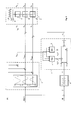
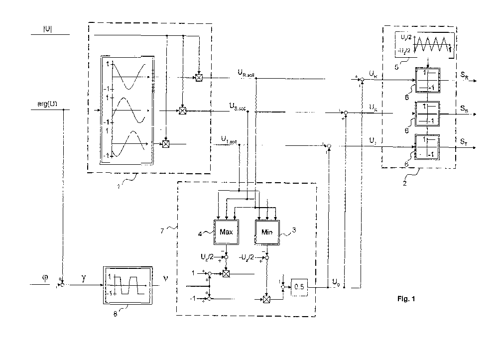
- FIG. 1 is a block diagram of the control device according to the invention and the Tax procedure shown.
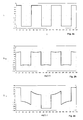
- FIG. 2a shows a value table of the function memory 8 which has jumps
- FIG. 2b shows the course of the zero-voltage system (U 0 , U 0 , U 0 ) belonging to FIG. 2a, the nominal voltage having a small amount.
- the resulting voltage profile of phase R of the resulting voltage system is shown in FIG. 2c.
- FIG. 3a shows a value table of the function memory 8 which has jumps;
- FIG. 3b shows the course of the zero voltage system (U 0 , U 0 , U 0 ) belonging to FIG. 3a, the target voltage having a large amount.
- the resulting voltage profile of phase R of the resulting voltage system is shown in FIG. 3c.
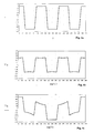
- FIG. 4a shows a table of values of the function memory 8 with a continuous function curve
- FIG. 4b shows the curve of the zero-voltage system (U 0 , U 0 , U 0 ) belonging to FIG. 4a, the nominal voltage having a small amount
- FIG. 4c shows the resulting voltage curve of phase R of the resulting voltage system.
- FIG. 5a shows a table of values of the function memory 8 with a continuous function curve
- FIG. 5b shows the curve of the zero-voltage system (U 0 , U 0 , U 0 ) belonging to FIG. 5a, the target voltage having a large amount
- FIG. 5c shows the resulting voltage curve of phase R of the resulting voltage system.
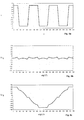
- FIG. 6a shows a value table of the function memory 8 with a continuous function curve
- FIG. 6b shows the curve of the zero-voltage system (U 0 , U 0 , U 0 ) belonging to FIG. 6a, the target voltage having a large amount and an optimized one Head angle is used.
- FIG. 6c shows the resulting voltage curve of phase R of the resulting voltage system.
- the function generator 1 forms from the voltage space pointer, which is determined by the amount
- U R , Soll, U S, Soll, U T, Soll a target voltage system
- U 0 , U 0 , U 0 is added up.
- the resulting voltage system (U R , U S , U T ) is fed to a pulse width modulator 2.
- the triangular voltage of the function generator 5 is compared by comparators 6 with the resulting voltage system (U R , U S , U T ).
- the pulse width modulator 2 is operated in such a way that with positive and negative full modulation of a phase of the resulting voltage system (U R , U S , U T ) there is no switching of the switching signal within a modulation period of the pulse width modulator 2.
- the zero voltage system (U 0 , U 0 , U 0 ) is formed by the arithmetic unit 7 from the target voltage system (U R, Soll, U S, Soll, U T, Soll) and the control variable ⁇ .
- the control variable v results as the output value of the function memory 8, which has the input variable ⁇ , which represents the sum of the angle of the voltage space vector and the control angle ⁇ .
- the control angle ⁇ is offered by a higher-level control system, which is either voltage-controlled or current-controlled.
- the arithmetic unit 7 comprises a minimum value generator 3 and a maximum value generator 4, which form a minimum value or a maximum value from the target voltage system (U R, Soll, U S, Soll , U T, Soll).
- the maximum zero voltage is determined from the difference between U Z / 2 and the maximum value formed.
- the minimum zero voltage is also determined from the difference between -U Z / 2 and the minimum value formed.
- the maximum zero voltage is multiplied by the control variable ⁇ increased by 1.
- the minimum zero voltage is multiplied by the control variable ⁇ reduced by 1. After halving, the difference between the two multiplication results results in the voltage U 0 , from which the zero-voltage system (U 0 , U 0 , U 0 ) is formed.
- the rising and falling edges of those in the functional memory 8 are particularly characteristic entered function. They do not run vertically, i.e. with an infinite slope, as in a switch or the like, but with a finite slope. So that limits Angular ranges of maximum or minimum zero-voltage components are not immediate to each other, but are finite incline from each other due to additional angular ranges separated, in which a continuous transition from minimum zero voltage component to maximum Zero voltage component and vice versa takes place.
- the scalar voltage U 0 of the zero-voltage system (U 0 , U 0 , U 0 ) can assume values between U z / 2 or -U z / 2.
- the cycle time that is to say the time difference between two successive time steps, is 250 ⁇ s.
- the characteristic value 'voltage change per time' of the time profile of U 0 is particularly characteristic when it comes to noise generation, since louder noises are produced when there is a rapid, large voltage change than when there is a slow, small voltage change per time step or cycle time of the time-discrete system.
- a value for the characteristic value is voltage change can be specified per time and is used to determine the course of the function table.
- the flattop areas can be shifted so that they with regard to the output currents are as close as possible to their maximum, which is the Effectiveness in saving switching losses increases, especially if the Angle is continuously adapted to the operating point of the engine.
- An arithmetic logic unit 7 is connected downstream of the function memory 8 and calculates the voltage U 0 from instantaneous values of the maximum and minimum phase potential, as well as the instantaneous intermediate circuit voltage U z and the output value of the function memory ⁇ according to the following formula:
- FIG. 2a shows a value table of the function memory 8 with abrupt transitions that correspond to a switching behavior. This is stored in the function memory 8 and the angle ⁇ is set to zero. This results in a 60 ° flattop method, in which the flattop angle ranges are arranged symmetrically around a maximum or a minimum of one phase of the target voltage system.
- FIG. 2b shows the associated course of the voltage U 0 , the magnitude of the voltage space vector
- FIG. 2c shows the associated voltage curve of phase R of the resulting voltage system.
- FIGS. 3a, 3b, 3c show the same corresponding sizes as in the figures 2a, 2b, 2c, but with
- 250V. This is why all the courses also show erratic changes Transitions or jump points, which in turn contribute to increasing noise as well as in Figures 2a, 2b, 2c.
- FIG. 4a shows a table of values of the function memory 8 with continuous transitions which extend over 10 ° in each case.
- the table also shows a non-negligible amount of intermediate values between -1 and 1. Depending on the speed and the cycle time for a time-discrete version, a different number of these intermediate values are used.
- FIG. 4b shows the associated profile of the voltage U 0 of the zero-voltage system, with
- FIG. 4c shows the voltage curve of phase R of the resulting voltage system, which is associated with FIG. 4a. All the courses in FIGS. 4a, 4b, 4c do not have abrupt, but rather continuous transitions. In any case, the voltage change per time is below a finite limit and is therefore limited. The noise generation is thus suppressed or at least reduced.
- 5a, 5b, 5c show the same corresponding sizes as in the figures 4a, 4b, 4c, but with
- 250V. Again, all courses show continuous transitions and have an effect thus also a reduction in noise.
- FIG. 6a again shows a table of values of the function memory 8 with continuous transitions which extend over 10 ° in each case.
- FIG. 6b shows the associated course of the voltage U 0 , where
- FIG. 6c also shows the course of the voltage U R of the phase R and an example of the course of the current I R of the phase R, which has a phase shift angle of 30 ° with respect to the voltage U R.
- FIG. 6c shows the voltage curve of phase R of the resulting voltage system belonging to FIG. 6a, the position of the described flattop angle ranges and the curve of the current of the corresponding phase R.
- the invention thus combines the advantages of reduced switching losses with reduced ones Noise.
- converters such as for example, multi-level converters.
Landscapes
- Engineering & Computer Science (AREA)
- Power Engineering (AREA)
- Dc-Dc Converters (AREA)
- Inverter Devices (AREA)
- Ac-Ac Conversion (AREA)
- Electrical Discharge Machining, Electrochemical Machining, And Combined Machining (AREA)
- Selective Calling Equipment (AREA)
Abstract
- ersten Winkelbereichen, bei denen ein maximales Nullspannungssystem (U0,MAX, U0,MAX, U0,MAX) aufsummiert wird,
- zweiten Winkelbereichen, bei denen ein minimales Nullspannungssystem (U0,MIN, U0,MIN, U0,MIN) aufsummiert wird und
- dritten Winkelbereichen, bei denen ein zwischen minimalem und maximalem Nullspannungssystem liegendes Nullspannungssystem aufsummiert wird,
Description
- ersten Winkelbereichen, bei denen ein maximales Nullspannungssystem (U0,MAX, U0,MAX, U0,MAX) aufsummiert wird,
- zweiten Winkelbereichen, bei denen ein minimales Nullspannungssystem (U0,MIN, U0,MIN, U0,MIN) aufsummiert wird und
- dritten Winkelbereichen, bei denen ein zwischen minimalem und maximalem Nullspannungssystem liegendes Nullspannungssystem aufsummiert wird,
- erste Winkelbereiche, bei denen ein maximales Nullspannungssystem (U0,MAX, U0,MAX, U0,MAX) aufsummiert wird,
- zweite Winkelbereiche, bei denen ein minimales Nullspannungssystem (U0,MIN, U0,MIN, U0,MIN) aufsummiert wird und
- dritte Winkelbereiche, bei denen ein zwischen minimalem und maximalem Nullspannungssystem liegendes Nullspannungssystem aufsummiert wird,

Von Vorteil ist dabei, dass durch Verwendung der beschriebenen Steuerverfahren kein direkter Übergang von ersten zu zweiten Winkelbereichen vorliegt und damit auch kein Sprung vom minimalem zum maximalen Nullspannungssystem oder umgekehrt vorliegt, wodurch kein Knackgeräusch, Summen oder anderes Geräusch entsteht. Außerdem ist das Verhalten des Nullspannungssystems in den dritten Winkelbereichen derart wählbar, dass die Spannungsänderung pro Zeit immer unter einem kritischen Wert bleibt, ab dem eine hörbare Geräuschbildung oder eine störende Geräuschbildung auftritt. Außerdem ist die Lösung kostengünstig als Software realisierbar. Darüber hinaus werden Schaltverluste in den steuerbaren Leistungshalbleiter-Schaltern eines pulsdauermodulierten Umrichters reduziert, ohne dass eine unerwünschte Geräuschbildung auftritt. Zusätzlich wird auch eine sonst bekannte Vorrichtung nur um die erfindungsgemäß notwendigen Mittel zur Bildung des Rechenwerks und Funktionsspeichers erweitert.
- 1
- Funktionsgenerator
- 2
- Pulsweitenmodulator
- 3
- Minimalwertbildner
- 4
- Maximalwertbildner
- 5
- Funktionsgenerator für Dreieckspannung
- 6
- Komparator
- 7
- Rechenwerk
- 8
- Funktionsspeicher
Der Steuerwinkel ϕ wird von einer übergeordneten Regelung angeboten, die entweder spannungsgeführt oder stromgeregelt ausgeführt ist.

In der Figur 4c ist wiederum der zu Figur 4a gehörige Spannungsverlauf der Phase R des resultierenden Spannungssystems gezeigt. Alle Verläufe der Figuren 4a, 4b, 4c weisen keine sprunghaften, sondern stetige Übergänge auf. In jedem Fall ist die Spannungsänderung pro Zeit unterhalb eines endlichen Grenzwertes und somit beschränkt. Die Geräuschbildung ist somit unterdrückt oder zumindest reduziert.
Claims (10)
- Steuerverfahren für einen pulsweitengesteuerten Umrichter mit steuerbaren Leistungshalbleiterschaltern zur Reduzierung von Schaltverlusten unter Vermeidung von Geräuschbildung,
wobei aus einem Spannungsraumzeiger, umfassend Betrag |U| und Winkel arg(U), ein Soll-Spannungssystem (UR,soll, US,soll, UT,soll) gebildet wird,
und wobei ein Nullspannungssystem (U0, U0, U0) aus dem Soll-Spannungssystem (UR,soll, US,soll, UT,soll), dem Winkel arg(U) und einem Steuerwinkel ϕ gebildet wird,
und wobei das aus der Summe von Nullspannungssystem (U0, U0, U0) und Soll-Spannungssystem (UR,soll, US,soll, UT,soll) resultierende Spannungssystem (UR, US, UT) einem Pulsweitenmodulator 2 zur Bildung der Steuersignale (SR, SS, ST) für die Leistungshalbleiterschalter des Umrichters zugeführt wird,
wobei der 360°-Winkelbereich des Sollspannungszeigers (UR,soll, US,soll, UT,soll) zusammengesetzt wird ausund wobei die ersten und die zweiten stets nur dritte Winkelbereiche zum Nachbarn haben.ersten Winkelbereichen, bei denen ein maximales Nullspannungssystem (U0,MAX, U0,MAX, U0,MAX) aufsummiert wird,zweiten Winkelbereichen, bei denen ein minimales Nullspannungssystem (U0,MIN, U0,MIN, U0,MIN) aufsummiert wird unddritten Winkelbereichen, bei denen ein zwischen minimalem und maximalem Nullspannungssystem liegendes Nullspannungssystem aufsummiert wird, - Steuerverfahren nach Anspruch 1,
dadurch gekennzeichnet, dass
die dritten Winkelbereiche einen quasistetigen Übergang von minimalem zum maximalem Nullspannungssystem und/oder umgekehrt darstellen. - Steuerverfahren nach einem der Ansprüche 1 bis 2,
dadurch gekennzeichnet, dass
die Spannung U0 des Nullspannungssystems (U0, U0, U0) in den dritten Winkelbereichen diskrete Werte annimmt. - Steuerverfahren nach Anspruch 3,
dadurch gekennzeichnet, dass
zumindest die maximale Differenz zweier zeitlich aufeinander folgenden Werte als Kennwert vorgebbar ist. - Steuerverfahren nach mindestens einem der vorangegangenen Ansprüche,
dadurch gekennzeichnet, dass
die dritten Winkelbereiche jeweils sich über mindestens 3° und/oder maximal 30° ausdehnen,
und/oder dass
die dritten Winkelbereiche jeweils sich über 10° ausdehnen,
und/oder dass
der Steuerwinkel ϕ von einer übergeordneten, strom- oder spannungsgeführten Steuerung vorgegeben wird,
und/oder dass
der Steuerwinkel ϕ konstant vorgegeben wird,
und/oder dass
der Steuerwinkel ϕ eine Funktion des Winkels zwischen Strom-Raumzeiger und Spannungs-Raumzeiger ist,
und/oder dass
der Steuerwinkel ϕ auf einen Winkelbereich begrenzt wird,
und/oder dass
der Winkelbereich sich über 60° erstreckt,
und/oder dass
ein Funktionsspeicher 8 aus der Summe von Steuerwinkel ϕ und von arg(U) eine Steuergröße ν zur Beeinflussung des Nullspannungssystem (U0, U0, U0) bildet unter Verwendung einer Funktion und/oder Funktionstabelle,
und/oder dass
die Funktion und/oder Funktionstabelleaufweisterste Winkelbereiche, bei denen ein maximales Nullspannungssystem (U0,MAX, U0,MAX, U0,MAX) aufsummiert wird,zweite Winkelbereiche, bei denen ein minimales Nullspannungssystem (U0,MIN, U0,MIN, U0,MIN) aufsummiert wird unddritte Winkelbereiche, bei denen ein zwischen minimalem und maximalem Nullspannungssystem liegendes Nullspannungssystem aufsummiert wird,
und dass die ersten und die zweiten stets nur dritte Winkelbereiche zum Nachbarn haben,
und/oder dass
im Rechenwerk 7 die Spannung U0 zur Bildung des Nullspannungssystems nach der Formelbestimmt wird, wobei UZ die Zwischenkreisspannung des Umrichters darstellt.
- Steuervorrichtung zur Durchführung eines Steuerverfahrens nach mindestens einem der vorangegangenen Ansprüche,
wobei die Steuervorrichtung von einem pulsweitengesteuerten Umrichter mit steuerbaren Leistungshalbleiterschaltern umfasst wird,
wobei ein Funktionsgenerator 1 aus einem Spannungsraumzeiger, umfassend Betrag |U| und Winkel arg(U), ein Soll-Spannungssystem (UR,soll, US,soll, UT,soll) bildet,
und wobei ein Rechenwerk 7 zusammen mit einem Funktionsspeicher 8 ein Nullspannungssystem (U0, U0, U0) aus dem Soll-Spannungssystem (UR,soll, US,soll, UT,soll), dem Winkel arg(U) und einem Steuerwinkel ϕ bildet,
und wobei ein Pulsweitenmodulator 2 aus der Summe von Nullspannungssystem (U0, U0, U0) und Soll-Spannungssystem (UR,soll, US,soll, UT,soll) Schaltsignale für Leistungshalbleiterschalter bildet. - Steuervorrichtung nach Anspruch 15,
dadurch gekennzeichnet, dass
der Umrichter Mittel zum Vorgeben des Steuerwinkels ϕ aufweist. - Steuervorrichtung nach Anspruch 16,
dadurch gekennzeichnet, dass
die Mittel durch eine übergeordnete, strom- oder spannungsgeführte Steuerung realisiert sind und/oder dass die Mittel zum Vorgeben des Steuerwinkels ϕ Eingabemittel sind. - Steuervorrichtung nach mindestens einem der vorangegangenen Ansprüche,
dadurch gekennzeichnet, dass
das Rechenwerk mindestens einen Minimalwertbildner 3 und mindestens einen Maximalwertbildner 4 aufweist. - Steuervorrichtung nach mindestens einem der vorangegangenen Ansprüche,
dadurch gekennzeichnet, dass
der Ausgangswert des Funktionsspeichers 8 im Rechenwerk 7 einem ersten und einem zweiten Addierer zugeführt wird
und/oder dass
die Addierer derart gestaltet sind, dasszur Bildung des Ausgangswerts des ersten Addierers auf den Ausgangswert des Funktionsspeichers 8 ein positiver Wert, wie 1 oder dergleichen, addiert wird und dasszur Bildung des Ausgangswerts des zweiten Addierers auf den Ausgangswert des Funktionsspeichers ein negativer Wert, wie -1 oder dergleichen, addiert wird und dassund dass die Ausgangswerte der Multiplizierer einem Subtrahierer zur Differenzbildung zugeführt werden und diese Differenz einem Multiplizierer oder einem Proportionalglied zur Bildung der Spannung U0 zugeführt wird.der Ausgangswert des ersten Addiererers mit der Differenz von UZ/2 und Ausgangswert des Maximalwertbildners unter Verwendung eines ersten Multiplizierers multipliziert wird,der Ausgangswert des zweiten Addiererers mit der Differenz von -UZ/2 und Ausgangswert des Minimalwertbildners unter Verwendung eines zweiten Multiplizierers multipliziert wird,
Applications Claiming Priority (2)
| Application Number | Priority Date | Filing Date | Title |
|---|---|---|---|
| DE10019374A DE10019374C2 (de) | 2000-04-18 | 2000-04-18 | Steuerverfahren für einen pulsweitengesteuerten Umrichter und eine Steuervorrichtung zur Durchführung dieses Steuerverfahrens |
| DE10019374 | 2000-04-18 |
Publications (3)
| Publication Number | Publication Date |
|---|---|
| EP1148629A2 true EP1148629A2 (de) | 2001-10-24 |
| EP1148629A3 EP1148629A3 (de) | 2002-07-24 |
| EP1148629B1 EP1148629B1 (de) | 2004-02-11 |
Family
ID=7639298
Family Applications (1)
| Application Number | Title | Priority Date | Filing Date |
|---|---|---|---|
| EP01106236A Expired - Lifetime EP1148629B1 (de) | 2000-04-18 | 2001-03-14 | Steuerverfahren für einen pulsweitengesteuerten Umrichter und Steuervorrichtung zur Durchführung dieses Steuerverfahrens |
Country Status (3)
| Country | Link |
|---|---|
| EP (1) | EP1148629B1 (de) |
| AT (1) | ATE259552T1 (de) |
| DE (2) | DE10019374C2 (de) |
Cited By (3)
| Publication number | Priority date | Publication date | Assignee | Title |
|---|---|---|---|---|
| WO2008135125A1 (de) * | 2007-05-04 | 2008-11-13 | Sew-Eurodrive Gmbh & Co. Kg. | Pwm-umrichter mit sollspannungskorrektor durch die nullsystemspannung zur reduzierung von schaltverlusten und der vermeidung von geräuschbildung |
| US8853990B2 (en) | 2011-03-15 | 2014-10-07 | Kabushiki Kaisha Toyota Jidoshokki | Inverter device of rotating electrical machine, and driving method for rotating electrical machine |
| WO2017125154A1 (en) * | 2016-01-21 | 2017-07-27 | Vacon Oy | Frequency converter with lcl line and common mode filter |
Families Citing this family (2)
| Publication number | Priority date | Publication date | Assignee | Title |
|---|---|---|---|---|
| US7061134B2 (en) * | 2003-08-01 | 2006-06-13 | General Motors Corporation | Method and system for improved thermal management of a voltage source inverter operating at low output frequency utilizing a zero vector modulation technique |
| DE102024138019B3 (de) | 2024-12-16 | 2026-04-23 | Diehl Ako Stiftung & Co. Kg | Verfahren zum Erzeugen eines Steuersignals für eine Pulsweitenmodulation, Konverter und Computerprogrammprodukt |
Family Cites Families (4)
| Publication number | Priority date | Publication date | Assignee | Title |
|---|---|---|---|---|
| DE2705343C2 (de) * | 1977-02-09 | 1985-10-17 | Brown, Boveri & Cie Ag, 6800 Mannheim | Steuerverfahren für einen selbstgeführten, pulsgesteuerten Wechselrichter und Steueranordnung zur Bildung der Sollwerte für die Pulssteuerung |
| US5475581A (en) * | 1994-06-10 | 1995-12-12 | Westinghouse Electric Corp. | Waveform flat-topping unit |
| DE4434342B4 (de) * | 1994-09-26 | 2009-01-02 | Siemens Ag | Steuerverfahren und Vorrichtung zur Reduzierung von Durchlaßspitzenwertverlusten in Leistungshalbleiter-Schaltern |
| US6058031A (en) * | 1997-10-23 | 2000-05-02 | General Electric Company | Five level high power motor drive converter and control system |
-
2000
- 2000-04-18 DE DE10019374A patent/DE10019374C2/de not_active Expired - Lifetime
-
2001
- 2001-03-14 DE DE50101461T patent/DE50101461D1/de not_active Expired - Lifetime
- 2001-03-14 AT AT01106236T patent/ATE259552T1/de not_active IP Right Cessation
- 2001-03-14 EP EP01106236A patent/EP1148629B1/de not_active Expired - Lifetime
Cited By (5)
| Publication number | Priority date | Publication date | Assignee | Title |
|---|---|---|---|---|
| WO2008135125A1 (de) * | 2007-05-04 | 2008-11-13 | Sew-Eurodrive Gmbh & Co. Kg. | Pwm-umrichter mit sollspannungskorrektor durch die nullsystemspannung zur reduzierung von schaltverlusten und der vermeidung von geräuschbildung |
| US8853990B2 (en) | 2011-03-15 | 2014-10-07 | Kabushiki Kaisha Toyota Jidoshokki | Inverter device of rotating electrical machine, and driving method for rotating electrical machine |
| WO2017125154A1 (en) * | 2016-01-21 | 2017-07-27 | Vacon Oy | Frequency converter with lcl line and common mode filter |
| CN108496302A (zh) * | 2016-01-21 | 2018-09-04 | 伟肯有限公司 | 具有lcl线路和共模滤波器的频率转换器 |
| US10270367B2 (en) | 2016-01-21 | 2019-04-23 | Vacon Oy | Frequency converter with LCL line and common mode filter |
Also Published As
| Publication number | Publication date |
|---|---|
| DE10019374C2 (de) | 2003-06-18 |
| ATE259552T1 (de) | 2004-02-15 |
| EP1148629A3 (de) | 2002-07-24 |
| DE10019374A1 (de) | 2001-10-31 |
| DE50101461D1 (de) | 2004-03-18 |
| EP1148629B1 (de) | 2004-02-11 |
Similar Documents
| Publication | Publication Date | Title |
|---|---|---|
| EP2156545B1 (de) | Pwm-umrichter mit sollspannungskorrektur durch die nullsystemspannung zur reduzierung von schaltverlusten und der vermeidung von geräuschbildung | |
| DE3816444C2 (de) | ||
| EP0356547B1 (de) | Verfahren zum Betrieb eines Dreipunktwechselrichters | |
| DE3852330T2 (de) | Pulsbreitenmodulierter Leistungskonverter. | |
| EP2348627A1 (de) | Wandlerschaltung sowie Verfahren zum Betreiben einer mehrstufigen Wandlerschaltung | |
| DE112013006977T5 (de) | Stromrichter | |
| DE112013006976T5 (de) | Steuereinheit eines elektrischen Wechselstrommotors | |
| DE112017004887T5 (de) | Umrichtersteuerverfahren, steuervorrichtung und umwandler | |
| EP0685940A1 (de) | Pulsweitenmodulierter Schaltwandler zum Betrieb elektrischer Verbraucher | |
| DE10060429A1 (de) | Verfahren und Vorrichtung zur Leistungsübertragung | |
| DE112005000294T5 (de) | Motorantriebsvorrichtung | |
| DE3012330A1 (de) | Impulsbreitenmodulierter wechselrichter und betriebsverfahren | |
| EP3504781A1 (de) | Regelung eines ausgangsstroms eines stromrichters | |
| EP1148629B1 (de) | Steuerverfahren für einen pulsweitengesteuerten Umrichter und Steuervorrichtung zur Durchführung dieses Steuerverfahrens | |
| WO2019192770A1 (de) | Antriebssteuerung für einen drehstrommotor | |
| EP3476035B1 (de) | Regelung von phasenströmen eines wechselrichters | |
| EP3095178B1 (de) | Modulare stromrichterschaltung mit submodulen, die im linearbetrieb betrieben werden | |
| EP3353885B1 (de) | Verfahren zum betrieb eines modularen multilevel-stromrichters, modularer multilevel-stromrichter sowie computerprogramm | |
| AT519842A1 (de) | Wechselrichter | |
| EP3482488B1 (de) | Regelung von phasenströmen parallel geschalteter wechselrichter | |
| DE4434342B4 (de) | Steuerverfahren und Vorrichtung zur Reduzierung von Durchlaßspitzenwertverlusten in Leistungshalbleiter-Schaltern | |
| EP3556003B1 (de) | Multilevelumrichter sowie verfahren zu dessen betrieb | |
| DE112015000929T5 (de) | Einrichtung und Verfahren zum Reduzieren von Oberschwingungen | |
| EP3871326B1 (de) | Selbstgeführter wechselrichter und dessen betreiben | |
| DE102024138019B3 (de) | Verfahren zum Erzeugen eines Steuersignals für eine Pulsweitenmodulation, Konverter und Computerprogrammprodukt |
Legal Events
| Date | Code | Title | Description |
|---|---|---|---|
| PUAI | Public reference made under article 153(3) epc to a published international application that has entered the european phase |
Free format text: ORIGINAL CODE: 0009012 |
|
| AK | Designated contracting states |
Kind code of ref document: A2 Designated state(s): AT BE CH CY DE DK ES FI FR GB GR IE IT LI LU MC NL PT SE TR |
|
| AX | Request for extension of the european patent |
Free format text: AL;LT;LV;MK;RO;SI |
|
| PUAL | Search report despatched |
Free format text: ORIGINAL CODE: 0009013 |
|
| RIC1 | Information provided on ipc code assigned before grant |
Free format text: 7H 02M 7/525 A, 7H 02M 7/48 B |
|
| AK | Designated contracting states |
Kind code of ref document: A3 Designated state(s): AT BE CH CY DE DK ES FI FR GB GR IE IT LI LU MC NL PT SE TR |
|
| AX | Request for extension of the european patent |
Free format text: AL;LT;LV;MK;RO;SI |
|
| 17P | Request for examination filed |
Effective date: 20030124 |
|
| AKX | Designation fees paid |
Designated state(s): AT BE CH CY DE DK ES FI FR GB GR IE IT LI LU MC NL PT SE TR |
|
| GRAP | Despatch of communication of intention to grant a patent |
Free format text: ORIGINAL CODE: EPIDOSNIGR1 |
|
| RAP1 | Party data changed (applicant data changed or rights of an application transferred) |
Owner name: SEW-EURODRIVE GMBH & CO. KG |
|
| GRAS | Grant fee paid |
Free format text: ORIGINAL CODE: EPIDOSNIGR3 |
|
| GRAA | (expected) grant |
Free format text: ORIGINAL CODE: 0009210 |
|
| AK | Designated contracting states |
Kind code of ref document: B1 Designated state(s): AT BE CH CY DE DK ES FI FR GB GR IE IT LI LU MC NL PT SE TR |
|
| PG25 | Lapsed in a contracting state [announced via postgrant information from national office to epo] |
Ref country code: IT Free format text: LAPSE BECAUSE OF FAILURE TO SUBMIT A TRANSLATION OF THE DESCRIPTION OR TO PAY THE FEE WITHIN THE PRESCRIBED TIME-LIMIT;WARNING: LAPSES OF ITALIAN PATENTS WITH EFFECTIVE DATE BEFORE 2007 MAY HAVE OCCURRED AT ANY TIME BEFORE 2007. THE CORRECT EFFECTIVE DATE MAY BE DIFFERENT FROM THE ONE RECORDED. Effective date: 20040211 Ref country code: FI Free format text: LAPSE BECAUSE OF FAILURE TO SUBMIT A TRANSLATION OF THE DESCRIPTION OR TO PAY THE FEE WITHIN THE PRESCRIBED TIME-LIMIT Effective date: 20040211 Ref country code: TR Free format text: LAPSE BECAUSE OF FAILURE TO SUBMIT A TRANSLATION OF THE DESCRIPTION OR TO PAY THE FEE WITHIN THE PRESCRIBED TIME-LIMIT Effective date: 20040211 Ref country code: CY Free format text: LAPSE BECAUSE OF FAILURE TO SUBMIT A TRANSLATION OF THE DESCRIPTION OR TO PAY THE FEE WITHIN THE PRESCRIBED TIME-LIMIT Effective date: 20040211 Ref country code: NL Free format text: LAPSE BECAUSE OF FAILURE TO SUBMIT A TRANSLATION OF THE DESCRIPTION OR TO PAY THE FEE WITHIN THE PRESCRIBED TIME-LIMIT Effective date: 20040211 Ref country code: IE Free format text: LAPSE BECAUSE OF FAILURE TO SUBMIT A TRANSLATION OF THE DESCRIPTION OR TO PAY THE FEE WITHIN THE PRESCRIBED TIME-LIMIT Effective date: 20040211 |
|
| REG | Reference to a national code |
Ref country code: GB Ref legal event code: FG4D Free format text: NOT ENGLISH |
|
| REG | Reference to a national code |
Ref country code: CH Ref legal event code: EP |
|
| REG | Reference to a national code |
Ref country code: IE Ref legal event code: FG4D Free format text: GERMAN |
|
| PG25 | Lapsed in a contracting state [announced via postgrant information from national office to epo] |
Ref country code: LU Free format text: LAPSE BECAUSE OF NON-PAYMENT OF DUE FEES Effective date: 20040314 Ref country code: AT Free format text: LAPSE BECAUSE OF NON-PAYMENT OF DUE FEES Effective date: 20040314 |
|
| GBT | Gb: translation of ep patent filed (gb section 77(6)(a)/1977) |
Effective date: 20040225 |
|
| REF | Corresponds to: |
Ref document number: 50101461 Country of ref document: DE Date of ref document: 20040318 Kind code of ref document: P |
|
| PG25 | Lapsed in a contracting state [announced via postgrant information from national office to epo] |
Ref country code: BE Free format text: LAPSE BECAUSE OF NON-PAYMENT OF DUE FEES Effective date: 20040331 Ref country code: MC Free format text: LAPSE BECAUSE OF NON-PAYMENT OF DUE FEES Effective date: 20040331 |
|
| PG25 | Lapsed in a contracting state [announced via postgrant information from national office to epo] |
Ref country code: SE Free format text: LAPSE BECAUSE OF FAILURE TO SUBMIT A TRANSLATION OF THE DESCRIPTION OR TO PAY THE FEE WITHIN THE PRESCRIBED TIME-LIMIT Effective date: 20040511 Ref country code: DK Free format text: LAPSE BECAUSE OF FAILURE TO SUBMIT A TRANSLATION OF THE DESCRIPTION OR TO PAY THE FEE WITHIN THE PRESCRIBED TIME-LIMIT Effective date: 20040511 Ref country code: GR Free format text: LAPSE BECAUSE OF FAILURE TO SUBMIT A TRANSLATION OF THE DESCRIPTION OR TO PAY THE FEE WITHIN THE PRESCRIBED TIME-LIMIT Effective date: 20040511 |
|
| PG25 | Lapsed in a contracting state [announced via postgrant information from national office to epo] |
Ref country code: ES Free format text: LAPSE BECAUSE OF FAILURE TO SUBMIT A TRANSLATION OF THE DESCRIPTION OR TO PAY THE FEE WITHIN THE PRESCRIBED TIME-LIMIT Effective date: 20040522 |
|
| NLV1 | Nl: lapsed or annulled due to failure to fulfill the requirements of art. 29p and 29m of the patents act | ||
| REG | Reference to a national code |
Ref country code: IE Ref legal event code: FD4D |
|
| BERE | Be: lapsed |
Owner name: SEW-EURODRIVE G.M.B.H. & CO. KG Effective date: 20040331 |
|
| ET | Fr: translation filed | ||
| PLBE | No opposition filed within time limit |
Free format text: ORIGINAL CODE: 0009261 |
|
| STAA | Information on the status of an ep patent application or granted ep patent |
Free format text: STATUS: NO OPPOSITION FILED WITHIN TIME LIMIT |
|
| 26N | No opposition filed |
Effective date: 20041112 |
|
| PG25 | Lapsed in a contracting state [announced via postgrant information from national office to epo] |
Ref country code: CH Free format text: LAPSE BECAUSE OF NON-PAYMENT OF DUE FEES Effective date: 20050331 Ref country code: LI Free format text: LAPSE BECAUSE OF NON-PAYMENT OF DUE FEES Effective date: 20050331 |
|
| REG | Reference to a national code |
Ref country code: CH Ref legal event code: PL |
|
| PG25 | Lapsed in a contracting state [announced via postgrant information from national office to epo] |
Ref country code: PT Free format text: LAPSE BECAUSE OF NON-PAYMENT OF DUE FEES Effective date: 20040711 |
|
| REG | Reference to a national code |
Ref country code: FR Ref legal event code: PLFP Year of fee payment: 16 |
|
| REG | Reference to a national code |
Ref country code: FR Ref legal event code: PLFP Year of fee payment: 17 |
|
| REG | Reference to a national code |
Ref country code: FR Ref legal event code: PLFP Year of fee payment: 18 |
|
| PGFP | Annual fee paid to national office [announced via postgrant information from national office to epo] |
Ref country code: GB Payment date: 20200304 Year of fee payment: 20 |
|
| PGFP | Annual fee paid to national office [announced via postgrant information from national office to epo] |
Ref country code: FR Payment date: 20200214 Year of fee payment: 20 |
|
| PGFP | Annual fee paid to national office [announced via postgrant information from national office to epo] |
Ref country code: DE Payment date: 20200331 Year of fee payment: 20 |
|
| REG | Reference to a national code |
Ref country code: DE Ref legal event code: R071 Ref document number: 50101461 Country of ref document: DE |
|
| REG | Reference to a national code |
Ref country code: GB Ref legal event code: PE20 Expiry date: 20210313 |
|
| PG25 | Lapsed in a contracting state [announced via postgrant information from national office to epo] |
Ref country code: GB Free format text: LAPSE BECAUSE OF EXPIRATION OF PROTECTION Effective date: 20210313 |