EP1148559A2 - High speed semiconductor photodetector and method of fabricating the same - Google Patents
High speed semiconductor photodetector and method of fabricating the same Download PDFInfo
- Publication number
- EP1148559A2 EP1148559A2 EP01250133A EP01250133A EP1148559A2 EP 1148559 A2 EP1148559 A2 EP 1148559A2 EP 01250133 A EP01250133 A EP 01250133A EP 01250133 A EP01250133 A EP 01250133A EP 1148559 A2 EP1148559 A2 EP 1148559A2
- Authority
- EP
- European Patent Office
- Prior art keywords
- layered
- semiconductor
- layer
- metal
- metal layer
- Prior art date
- Legal status (The legal status is an assumption and is not a legal conclusion. Google has not performed a legal analysis and makes no representation as to the accuracy of the status listed.)
- Withdrawn
Links
Images



Classifications
-
- H—ELECTRICITY
- H10—SEMICONDUCTOR DEVICES; ELECTRIC SOLID-STATE DEVICES NOT OTHERWISE PROVIDED FOR
- H10F—INORGANIC SEMICONDUCTOR DEVICES SENSITIVE TO INFRARED RADIATION, LIGHT, ELECTROMAGNETIC RADIATION OF SHORTER WAVELENGTH OR CORPUSCULAR RADIATION
- H10F77/00—Constructional details of devices covered by this subclass
- H10F77/10—Semiconductor bodies
- H10F77/14—Shape of semiconductor bodies; Shapes, relative sizes or dispositions of semiconductor regions within semiconductor bodies
- H10F77/147—Shapes of bodies
-
- H—ELECTRICITY
- H10—SEMICONDUCTOR DEVICES; ELECTRIC SOLID-STATE DEVICES NOT OTHERWISE PROVIDED FOR
- H10F—INORGANIC SEMICONDUCTOR DEVICES SENSITIVE TO INFRARED RADIATION, LIGHT, ELECTROMAGNETIC RADIATION OF SHORTER WAVELENGTH OR CORPUSCULAR RADIATION
- H10F30/00—Individual radiation-sensitive semiconductor devices in which radiation controls the flow of current through the devices, e.g. photodetectors
- H10F30/20—Individual radiation-sensitive semiconductor devices in which radiation controls the flow of current through the devices, e.g. photodetectors the devices having potential barriers, e.g. phototransistors
- H10F30/21—Individual radiation-sensitive semiconductor devices in which radiation controls the flow of current through the devices, e.g. photodetectors the devices having potential barriers, e.g. phototransistors the devices being sensitive to infrared, visible or ultraviolet radiation
- H10F30/22—Individual radiation-sensitive semiconductor devices in which radiation controls the flow of current through the devices, e.g. photodetectors the devices having potential barriers, e.g. phototransistors the devices being sensitive to infrared, visible or ultraviolet radiation the devices having only one potential barrier, e.g. photodiodes
- H10F30/221—Individual radiation-sensitive semiconductor devices in which radiation controls the flow of current through the devices, e.g. photodetectors the devices having potential barriers, e.g. phototransistors the devices being sensitive to infrared, visible or ultraviolet radiation the devices having only one potential barrier, e.g. photodiodes the potential barrier being a PN homojunction
- H10F30/2215—Individual radiation-sensitive semiconductor devices in which radiation controls the flow of current through the devices, e.g. photodetectors the devices having potential barriers, e.g. phototransistors the devices being sensitive to infrared, visible or ultraviolet radiation the devices having only one potential barrier, e.g. photodiodes the potential barrier being a PN homojunction the devices comprising active layers made of only Group III-V materials
-
- H—ELECTRICITY
- H10—SEMICONDUCTOR DEVICES; ELECTRIC SOLID-STATE DEVICES NOT OTHERWISE PROVIDED FOR
- H10F—INORGANIC SEMICONDUCTOR DEVICES SENSITIVE TO INFRARED RADIATION, LIGHT, ELECTROMAGNETIC RADIATION OF SHORTER WAVELENGTH OR CORPUSCULAR RADIATION
- H10F71/00—Manufacture or treatment of devices covered by this subclass
- H10F71/127—The active layers comprising only Group III-V materials, e.g. GaAs or InP
-
- H—ELECTRICITY
- H10—SEMICONDUCTOR DEVICES; ELECTRIC SOLID-STATE DEVICES NOT OTHERWISE PROVIDED FOR
- H10F—INORGANIC SEMICONDUCTOR DEVICES SENSITIVE TO INFRARED RADIATION, LIGHT, ELECTROMAGNETIC RADIATION OF SHORTER WAVELENGTH OR CORPUSCULAR RADIATION
- H10F77/00—Constructional details of devices covered by this subclass
- H10F77/20—Electrodes
- H10F77/206—Electrodes for devices having potential barriers
- H10F77/241—Electrodes for devices having potential barriers comprising ring electrodes
-
- Y—GENERAL TAGGING OF NEW TECHNOLOGICAL DEVELOPMENTS; GENERAL TAGGING OF CROSS-SECTIONAL TECHNOLOGIES SPANNING OVER SEVERAL SECTIONS OF THE IPC; TECHNICAL SUBJECTS COVERED BY FORMER USPC CROSS-REFERENCE ART COLLECTIONS [XRACs] AND DIGESTS
- Y02—TECHNOLOGIES OR APPLICATIONS FOR MITIGATION OR ADAPTATION AGAINST CLIMATE CHANGE
- Y02E—REDUCTION OF GREENHOUSE GAS [GHG] EMISSIONS, RELATED TO ENERGY GENERATION, TRANSMISSION OR DISTRIBUTION
- Y02E10/00—Energy generation through renewable energy sources
- Y02E10/50—Photovoltaic [PV] energy
- Y02E10/544—Solar cells from Group III-V materials
-
- Y—GENERAL TAGGING OF NEW TECHNOLOGICAL DEVELOPMENTS; GENERAL TAGGING OF CROSS-SECTIONAL TECHNOLOGIES SPANNING OVER SEVERAL SECTIONS OF THE IPC; TECHNICAL SUBJECTS COVERED BY FORMER USPC CROSS-REFERENCE ART COLLECTIONS [XRACs] AND DIGESTS
- Y02—TECHNOLOGIES OR APPLICATIONS FOR MITIGATION OR ADAPTATION AGAINST CLIMATE CHANGE
- Y02P—CLIMATE CHANGE MITIGATION TECHNOLOGIES IN THE PRODUCTION OR PROCESSING OF GOODS
- Y02P70/00—Climate change mitigation technologies in the production process for final industrial or consumer products
- Y02P70/50—Manufacturing or production processes characterised by the final manufactured product
Definitions
- the present invention generally relates to semiconductor photodetectors, and more specifically to a high speed semiconductor photodetector and a method of fabricating the photodetector.
- a semiconductor photodetector is formed in a mesa structure in which the light-sensitive area is separated from the pad electrode by a V-shaped groove. Because of the V-groove separation, a large surface area is obtained without increasing parasitic capacitance and hence high speed operation of the device is possible.
- TiPtAu is used for the pad electrode and metal lines. Wet and dry etching processes are available for etching the metal compound. However, because of the absence of appropriate etchant for the composition Pt if wet etching is employed and because of the difficulty to achieve constant etch rate if dry etching is used, a technique known as "liftoff process" is used, instead of the metal etching process.
- a thick layer of photoresist is patterned on the surface of the mesa structure and then a thin layer of metal is deposited using evaporation.
- the device is immersed in a solution capable of dissolving the photoresist.
- the pad and metal lines that were directly deposited on the semiconductor remain, while the metal deposited on the resist lifts off of the device as the resist dissolves.
- one shortcoming of the liftoff process is poor step coverage. Since the metal evaporation process has a directional characteristic, the metal deposited at stepped portions is thinned and tends to break under stress. Another shortcoming is that the Au of the deposited metal exhibits an undesirable characteristic because its high malleability causes a burr to occur when the metal on the photoresist is separated from the metal on the semiconductor. As a result, fifty percent of the metal lines actually produced has a poor configuration.
- Another object of the present invention is to provide a high speed semiconductor photodetector which can be manufactured with high yield and a method of fabricating the photodetector.
- a semiconductor photodetector comprising a semi-insulating substrate, a first layered-semiconductor mesa structure and a second layered-semiconductor mesa structure formed side by side on the substrate, the first layered-semiconductor mesa structure having a photoactive region and a first electrode on the photoactive region and the second layered-semiconductor mesa structure having a pad electrode, and an interconnect line of laminated metal structure for establishing a connection between the first electrode and the pad electrode.
- the laminated metal structure comprises a lower metal layer and an upper metal layer, the upper metal layer having a greater thickness than the thickness of the lower metal layer.
- the interconnect line extends along sidewalls of a valley between the first and second semiconductor mesa structures. In a modified embodiment, the interconnect line extends as a bridge over a void between the first and second semiconductor mesa structures.
- a method of fabricating a semiconductor photodetector comprising the steps of (a) forming a first layered-semiconductor mesa structure having a photoactive region and a second layered-semiconductor mesa structure side by side on a semi-insulating substrate, (b) enclosing the first and second layered-semiconductor mesa structures with a protective layer, (c) patterning the protective layer to form a contact hole therein and filling the contact hole with conductive material to form a first electrode on the photoactive region, (d) surrounding the first and second layered-semiconductor mesa structures with a photoresist layer by excluding an elongate portion that extends along sidewalls of a valley between the mesa structures, (e) covering the mesa structures and the surrounding photoresist layer with a metal layer, (f) forming on the metal layer a mask having patterns of the first electrode
- the present invention provides a modified method in which an air bridge process is used for fabricating the interconnect metal line.
- the modified method comprises the steps of (a) forming a first layered-semiconductor mesa structure having a photoactive region and a second layered-semiconductor mesa structure side by side on a semi-insulating substrate, (b) enclosing the first and second layered-semiconductor mesa structures with a protective layer, (c) patterning the protective layer to form a contact hole therein and filling the contact hole with conductive material to form a first electrode on the photoactive region, (d) surrounding the first and second layered-semiconductor mesa structures with a photoresist layer by filling a valley therebetween with the photoresist layer, (e) covering the mesa structures and the surrounding photoresist layer with a metal layer, (f) forming on the metal layer a mask having patterns of the first electrode, an elong
- the surrounding photoresist layer of the step (d) partially covers edge portions of the mesa structures, and the step (d) comprises the step of hard-baking the photoresist layer to form downwardly sloping contour at inner fringe portions of the surrounding photoresist layer.
- the step (h) is performed by using an ion milling process.
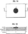
- a semiconductor photodetector of the present invention is shown in a sequence of fabrication stages according to a first embodiment of the present invention.
- a Fe-doped high-resistance InP semi-insulating substrate 101 with a thickness of 300 to 500 ⁇ m is used as a starting member.
- an n-type 1 ⁇ m thick InP buffer layer 102 is deposited with a carrier concentration of 1 x 10 18 cm -3 which is then covered with a undoped 2- ⁇ m thick InGaAs light absorbing layer 103 with a carrier concentration of 1 x 10 15 cm -3 .
- On the absorbing layer 103 is a 1- ⁇ m thick n-type InP cap layer 104 with a carrier concentration of 1 x 10 16 cm -3 .
- zinc is thermally diffused into the cap layer 104.
- the diffused region of the cap layer is converted to p-type InP to function as a photoactive region 105.
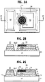
- the device is then selectively etched with a solution of bromine and methanol through a photoresist, not shown, until portions of the upper surface of semi-insulating substrate 101 are exposed to create two mesa structures, i.e., a light-sensitive portion 106 and a pad electrode portion 107 electrically separated by a steep valley from the photoactive region 105, as shown in Fig. 2B.
- the device is entirely coated with an SiN x protection film 110 using a plasma CVD method.
- the protection film 110 has a thickness of ⁇ /4n, where ⁇ is the wavelength of incident light and n is the refractive index of the protection film 110.
- Two contact holes are created in a portion of the protection film 110 which coats the photoactive mesa structure 106.
- One is a ring opening over the photoactive region 105 and the other is a rectangular opening on the cap layer 104 with one side having inwardly curved arc (see Figs. 2A and 2C).
- a 100-nm thick, ring-shaped positive contact electrode 108 formed of AnZn is deposited on the photoactive region 105, and a 100-nm thick, negative contact electrode 109 formed of AuGeNi is deposited on the cap layer 104.
- the device is then subjected to a sintering process in an H 2 environment.
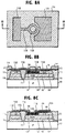
- the device is coated with a thick layer of novolac photoresist which is then exposed to an imagewise radiation so that it surrounds the steep edges of the mesa structures 106 and 107 as indicated by numeral 111.
- Photoresist layer 111 extends inwardly from the steep edges 112 of the mesa structures to cover edge portions of their upper surfaces. However, the photoresist layer 111 is not provided on a narrow region 112A of the steep valley in which an interconnect metal line is to be formed. The surrounding photoresist layer 111 is then hard-baked at a temperature of 160°C.
- the fringes of the mesa-surrounding resist layer 111 that extend inwards from the edges of the resist layer 111 are flattened and form a contour sloping downwards to the protected upper surface of the mesas portions 106 and 107 as indicated by 112B (Fig.3C).
- the device is entirely covered with a 150-nm thick metal film 113. This is done by consecutively evaporating Ti, Pt and Au, each with a thickness of 50 nanometers.
- Metal film 113 is coated with a thick photoresist layer, which is then subjected to an imagewise radiation so that the resist layer is patterned into a photomask 114.
- the photomask 114 is used as a mask to selectively deposit Au on the metal film 113 to form 1- ⁇ m thick metallized regions 115A, 115B, 115C and 115D.
- Metal film 115A has a pattern somewhat oversize of the negative contact electrode 109 that underlies the metal sheet 113 below the metallized region 115A, and the metallized region 115B is likewise oversize of the underlying positive, ring-shaped contact electrode 108.
- Metallized region 115C is a narrow strip that extends between the ring-shaped metal film 115B and the metallized region 115D which is formed in the shape of a rectangle on the surface of pad electrode mesa 107. Photomask 114 is then removed.
- the next step is an ion milling process in which Ar is used to remove unnecessary portions of the metal sheet by using the Au-metallized regions 115A to 115D as a mask (see Figs. 5A to 5C).
- the metal film 113 is segmented into a plurality of TiPtAu regions 113A, 113B, 113C and 113D of upper metallized regions 115A, 115B, 115C and 115D. It is seen that all of these metallized regions 115A to 115D form two-layered structures with underlying conductive regions 113A to 13D.
- the conductive region 115A establishes contact with the negative contact electrode 109 and the region 115D establishes contact with the positive ring-shaped contact electrode 108 via regions 115B and 115C.
- the conductive regions 115A and 115D are used as a negative and a positive electrode, respectively.
- Each of the positive and negative electrodes is thus formed with a two-layered laminated structure, with the upper metal layer 115 having a greater thickness than the thickness of the lower metal layer 113.
- Photoresist layer 111 is then removed as shown in Figs. 6A, 6B and 6C.
- the bottom surface of semi-insulating substrate 101 is polished to a depth of 150 ⁇ m and a rear-side electrode 120 is formed by consecutively evaporating AuGeNi/Ti/Au to respective thicknesses of 1000/500/2000 Angstrom.
- One feature of the laminated structure of the present invention is that an interconnect metal line of desired thickness can be deposited on the V-shaped steep valley between the two mesa structures even if the valley has steep sidewalls of more than 50 degrees to the horizontal. Since an increase in the thickness of the interconnect metal line results in a low line resistance which allows the photodetector to operate at high speeds. Further, the interconnect line is strengthened and possible line cuts and faults which might be caused by the mechanical stress of the valley structure are prevented.
- Another feature of the present invention is that, since the photoresist layer 114 is used as a mask for depositing the metallized Au-regions 115, precision patterning of the positive and negative electrodes is achieved. This avoids poor metal patterns associated with the liftoff method.
- a still further feature of the present invention is that the downwardly sloping fringes of the hard-baked mesa-surrounding resist layer 111 permit complete removal of the undesired edge portions of overlying metal patterns 113 with the use of the ion milling method which is characterized by its significant directionality. As a result, the electrodes can be formed with a greater degree of precision.
- a yield of more than 90 percent and a cutoff frequency of 15 GHz at a bias voltage of-5 volts were obtained for the photodetectors of the present invention.
- the interconnect metal line is fabricated according to the air bridge method.
- the same process is used as that of the previous embodiment until the protection coat 110 is formed. Therefore, the process steps shown in Figs. 1A to 2C is applied to this embodiment.
- Figs. 7A to 9C the process starting on the basis of Figs. 1A to 2C is illustrated.
- Photoresist layer 111 is deposited in a manner identical to the previous embodiment except that the valley between the two mesa structures is filled with the photoresist as seen from Figs. 7A and 7B. Similar to the previous embodiment, the device is hard-baked at 160°C to cause the resist layer 111 to form downwardly sloping fringes extending inwards from the edges of the upper surface of the mesa structures, as shown in Fig. 7C.
- the metal film 113 is deposited on the device by consecutively evaporating Ti, Pt and Au, each with a thickness of 50 nanometers, followed by the formation of the patterned photoresist layer 114 on the metal layer 113.
- the patterned resist layer 114 serves as a mask for metallizing the device with Au to form conductive regions 115A, 115B, 115E and 115D.
- the metal regions 115A, 115B, 115E, 115D are used as a mask for subjecting the device to an ion milling process using Ar to segment the underlying metal layer 113 into several regions 113A, 113B, 113E and 113D corresponding to the overlying metal regions 115A, 115B, 115E and 115D.
- the metal regions 113E and 115E form a bridge extending over the mesa-separating valley as dearly shown in Fig. 8C.
- a void is created below the two-layered metal bridge formed by metal lines 113E and 115E as shown in Figs. 9A, 9B and 9C.
- the rear electrode 120 is deposited in the same manner as the previous embodiment.
- the bridging interconnect metal line of the modified embodiment has an extra feature that it needs a smaller length for the interconnect between the mesa structures 106 and 107, regardless of the steepness of the sidewalls of the mesa-separating valley. This is beneficial for lowering the line resistance of the interconnect.
- a further feature of the bridging structure is that the presence of air below it, instead of the underlying protective layer 110 of the first embodiment, provides a lower line capacitance.
Landscapes
- Light Receiving Elements (AREA)
- Electrodes Of Semiconductors (AREA)
- Internal Circuitry In Semiconductor Integrated Circuit Devices (AREA)
Abstract
Description
Claims (13)
- A semiconductor photodetector comprising:a semi-insulating substrate;a first layered-semiconductor mesa structure and a second layered-semiconductor mesa structure formed side by side on said substrate, said first layered-semiconductor mesa structure having a photoactive region and a first electrode on said photoactive region and said second layered-semiconductor mesa structure having a pad electrode; andan interconnect line of laminated metal structure for establishing a connection between said first electrode and said pad electrode.
- The semiconductor photodetector of claim 1, wherein said laminated metal structure comprises a lower metal layer and an upper metal layer, the upper metal layer having a greater thickness than the thickness of said lower metal layer.
- The semiconductor photodetector of claim 1, wherein said interconnect line extends along sidewalls of a valley between said first and second semiconductor mesa structures.
- The semiconductor photodetector of claim 1, wherein said interconnect line extends as a bridge over a void between said first and second semiconductor mesa structures.
- The semiconductor photodetector of claim 1, wherein said first electrode is in the shape of a ring, and wherein said first layered-semiconductor mesa structure further includes a second electrode adapted to be biased at a potential opposite to a potential which will be applied to said first electrode when the photodetector is in operation.
- A method of fabricating a semiconductor photodetector comprising the steps of:a) forming a first layered-semiconductor mesa structure and a second layered-semiconductor mesa structure side by side on a semi-insulating substrate, said first layered-semiconductor mesa structure having a photoactive region;b) enclosing said first and second layered-semiconductor mesa structures with a protective layer;c) patterning said protective layer to form a contact hole therein and filling the contact hole with conductive material to form a first electrode on said photoactive region;d) surrounding said first and second layered-semiconductor mesa structures with a photoresist layer by excluding an elongate portion that extends along sidewalls of a valley between said mesa structures;e) covering said mesa structures and said surrounding photoresist layer with a metal layer;f) forming on the metal layer a mask having patterns of said first electrode, said elongate portion and a pad electrode on said second mesa structure;g) selectively depositing conductive material through said mask to form a plurality of metallized regions on said metal layer;h) removing said mask and patterning said metal layer into a plurality of metal regions corresponding to the metallized regions by using the metallized regions as a mask; andi) removing said surrounding photoresist layer.
- The method of claim 6, wherein said metallized regions has a greater thickness than the thickness of said metal layer.
- The method of claim 6, wherein said surrounding photoresist layer of the step (d) partially covers edge portions of said mesa structures, wherein the step (d) comprises the step of hard-baking said photoresist layer to form downwardly sloping contour at inner fringe portions of said surrounding photoresist layer.
- The method of claim 6, wherein the step (h) is performed by using an ion milling process.
- A method of fabricating a semiconductor photodetector comprising the steps of:a) forming a first layered-semiconductor mesa structure and a second layered-semiconductor mesa structure side by side on a semi-insulating substrate, said first layered-semiconductor mesa structure having a photoactive region;b) enclosing said first and second layered-semiconductor mesa structures with a protective layer;c) patterning said protective layer to form a contact hole therein and filling the contact hole with conductive material to form a first electrode on said photoactive region;d) surrounding said first and second layered-semiconductor mesa structures with a photoresist layer by filling a valley therebetween with the photoresist layer;e) covering said mesa structures and said surrounding photoresist layer with a metal layer;f) forming on the metal layer a mask having patterns of said first electrode, an elongate portion that crosses over said valley and a pad electrode on said second mesa structure;g) selectively depositing conductive material through said mask to form a plurality of metallized regions on said metal layer;h) removing said mask and patterning said metal layer into a plurality of metal regions corresponding to the metallized regions by using the metallized regions as a mask; andi) removing said surrounding photoresist layer.
- The method of claim 10, wherein said metallized regions has a greater thickness than the thickness of said metal layer.
- The method of claim 10, wherein said surrounding photoresist layer of the step (d) partially covers edge portions of said mesa structures, wherein the step (d) comprises the step of hard-baking said photoresist layer to form downwardly sloping contour at inner fringe portions of said surrounding photoresist layer.
- The method of claim 10, wherein the step (h) is performed by using an ion milling process.
Applications Claiming Priority (2)
| Application Number | Priority Date | Filing Date | Title |
|---|---|---|---|
| JP2000121052A JP2001298211A (en) | 2000-04-17 | 2000-04-17 | Semiconductor light receiving element and method of manufacturing the same |
| JP2000121052 | 2000-04-17 |
Publications (2)
| Publication Number | Publication Date |
|---|---|
| EP1148559A2 true EP1148559A2 (en) | 2001-10-24 |
| EP1148559A3 EP1148559A3 (en) | 2003-08-06 |
Family
ID=18631766
Family Applications (1)
| Application Number | Title | Priority Date | Filing Date |
|---|---|---|---|
| EP01250133A Withdrawn EP1148559A3 (en) | 2000-04-17 | 2001-04-14 | High speed semiconductor photodetector and method of fabricating the same |
Country Status (3)
| Country | Link |
|---|---|
| US (1) | US6501104B2 (en) |
| EP (1) | EP1148559A3 (en) |
| JP (1) | JP2001298211A (en) |
Families Citing this family (13)
| Publication number | Priority date | Publication date | Assignee | Title |
|---|---|---|---|---|
| JP4075442B2 (en) * | 2002-04-18 | 2008-04-16 | 沖電気工業株式会社 | Optical semiconductor device and manufacturing method thereof |
| US8541876B2 (en) * | 2005-09-30 | 2013-09-24 | Intel Corporation | Microelectronic package having direct contact heat spreader and method of manufacturing same |
| CN101341600B (en) | 2005-12-26 | 2012-11-28 | 日本电气株式会社 | Semiconductor optical device |
| JP5007636B2 (en) | 2007-09-18 | 2012-08-22 | 三菱電機株式会社 | Manufacturing method of semiconductor light receiving element |
| CN100541829C (en) * | 2007-10-31 | 2009-09-16 | 中国科学院上海技术物理研究所 | InGaAs low mesa linear array or area array infrared detector chip |
| WO2010035508A1 (en) * | 2008-09-29 | 2010-04-01 | 日本電気株式会社 | Semiconductor photoreceptor element and manufacturing method therefor |
| JP2013105975A (en) | 2011-11-16 | 2013-05-30 | Mitsubishi Electric Corp | Optical semiconductor device manufacturing method |
| US9386954B2 (en) * | 2013-03-15 | 2016-07-12 | Zyvex Labs, Llc | Method of fabricating a multi-electrode array |
| CN103236475B (en) * | 2013-04-16 | 2016-01-06 | 华南理工大学 | The electrode bridging method of the LED luminescence unit of deep trench isolation |
| CN111937164B (en) | 2018-04-06 | 2024-06-25 | 株式会社村田制作所 | Optical semiconductor element |
| TWI697078B (en) * | 2018-08-03 | 2020-06-21 | 欣興電子股份有限公司 | Package substrate structure and method of bonding using the same |
| CN110854141A (en) * | 2019-11-21 | 2020-02-28 | 中国电子科技集团公司第四十四研究所 | Monolithic integrated balanced photoelectric detector chip and manufacturing method thereof |
| JP7569646B2 (en) * | 2020-09-16 | 2024-10-18 | 浜松ホトニクス株式会社 | Light detection module and beat spectrometer |
Family Cites Families (4)
| Publication number | Priority date | Publication date | Assignee | Title |
|---|---|---|---|---|
| EP0437836B1 (en) * | 1989-12-27 | 1995-05-17 | Nec Corporation | Optical semiconductor device |
| JPH0582829A (en) * | 1991-09-19 | 1993-04-02 | Nec Corp | Semiconductor light receiving element |
| US6008506A (en) * | 1996-04-25 | 1999-12-28 | Nec Corporation | SOI optical semiconductor device |
| JPH1140823A (en) * | 1997-05-22 | 1999-02-12 | Fujitsu Ltd | Photodetector module |
-
2000
- 2000-04-17 JP JP2000121052A patent/JP2001298211A/en active Pending
-
2001
- 2001-04-14 EP EP01250133A patent/EP1148559A3/en not_active Withdrawn
- 2001-04-16 US US09/834,648 patent/US6501104B2/en not_active Expired - Fee Related
Also Published As
| Publication number | Publication date |
|---|---|
| JP2001298211A (en) | 2001-10-26 |
| EP1148559A3 (en) | 2003-08-06 |
| US20010030330A1 (en) | 2001-10-18 |
| US6501104B2 (en) | 2002-12-31 |
Similar Documents
| Publication | Publication Date | Title |
|---|---|---|
| US6734036B2 (en) | Semiconductor device and method of fabrication | |
| EP1148559A2 (en) | High speed semiconductor photodetector and method of fabricating the same | |
| US6458620B1 (en) | Semiconductor device and method for producing the same | |
| US5468656A (en) | Method of making a VCSEL | |
| US4949352A (en) | Laser manufacture | |
| US12100929B2 (en) | Semiconductor optical device and method for manufacturing the same | |
| JP2021009999A (en) | Surface emitting laser and method for manufacturing the same | |
| JP2006013484A (en) | Lid for wafer scale package and method for forming the same | |
| US5744857A (en) | Semiconductor device | |
| US20040084685A1 (en) | Semiconductor devices, and methods of manufacture of the same | |
| JP7530238B2 (en) | Semiconductor optical device and its manufacturing method | |
| CN115425112A (en) | A kind of highly reliable InP mesa photodetector and its preparation method | |
| US20020117680A1 (en) | Semiconductor device and method of manufacture of the semiconductor device | |
| US6197700B1 (en) | Fabrication method for bottom electrode of capacitor | |
| US12610630B2 (en) | Method of manufacturing a light-receiving element and light-receiving element | |
| JP2726204B2 (en) | Manufacturing method of semiconductor waveguide device | |
| US5618753A (en) | Method for forming electrodes on mesa structures of a semiconductor substrate | |
| JP2656860B2 (en) | Semiconductor light emitting device and method of manufacturing the same | |
| US5407859A (en) | Field effect transistor with landing pad | |
| KR100454074B1 (en) | Method of manufacturing image sensor for semiconductor device | |
| JP4072248B2 (en) | Manufacturing method of semiconductor device | |
| JPH08111565A (en) | Semiconductor optical device and manufacturing method | |
| JP2653131B2 (en) | Photoelectric conversion element | |
| JPS5825229A (en) | Manufacture of semiconductor device | |
| CN116936709A (en) | Miniature light-emitting chip and manufacturing method thereof |
Legal Events
| Date | Code | Title | Description |
|---|---|---|---|
| PUAI | Public reference made under article 153(3) epc to a published international application that has entered the european phase |
Free format text: ORIGINAL CODE: 0009012 |
|
| AK | Designated contracting states |
Kind code of ref document: A2 Designated state(s): AT BE CH CY DE DK ES FI FR GB GR IE IT LI LU MC NL PT SE TR |
|
| AX | Request for extension of the european patent |
Free format text: AL;LT;LV;MK;RO;SI |
|
| RAP1 | Party data changed (applicant data changed or rights of an application transferred) |
Owner name: NEC ELECTRONICS CORPORATION |
|
| PUAL | Search report despatched |
Free format text: ORIGINAL CODE: 0009013 |
|
| AK | Designated contracting states |
Designated state(s): AT BE CH CY DE DK ES FI FR GB GR IE IT LI LU MC NL PT SE TR |
|
| AX | Request for extension of the european patent |
Extension state: AL LT LV MK RO SI |
|
| 17P | Request for examination filed |
Effective date: 20030905 |
|
| AKX | Designation fees paid |
Designated state(s): DE FR |
|
| 17Q | First examination report despatched |
Effective date: 20040511 |
|
| STAA | Information on the status of an ep patent application or granted ep patent |
Free format text: STATUS: THE APPLICATION IS DEEMED TO BE WITHDRAWN |
|
| 18D | Application deemed to be withdrawn |
Effective date: 20040922 |