EP1146555A1 - Semiconductor device and production method therefor - Google Patents
Semiconductor device and production method therefor Download PDFInfo
- Publication number
- EP1146555A1 EP1146555A1 EP00906706A EP00906706A EP1146555A1 EP 1146555 A1 EP1146555 A1 EP 1146555A1 EP 00906706 A EP00906706 A EP 00906706A EP 00906706 A EP00906706 A EP 00906706A EP 1146555 A1 EP1146555 A1 EP 1146555A1
- Authority
- EP
- European Patent Office
- Prior art keywords
- insulating layer
- containing carbon
- fluorine
- hard mask
- layer
- Prior art date
- Legal status (The legal status is an assumption and is not a legal conclusion. Google has not performed a legal analysis and makes no representation as to the accuracy of the status listed.)
- Granted
Links
Images




Classifications
-
- H—ELECTRICITY
- H10—SEMICONDUCTOR DEVICES; ELECTRIC SOLID-STATE DEVICES NOT OTHERWISE PROVIDED FOR
- H10P—GENERIC PROCESSES OR APPARATUS FOR THE MANUFACTURE OR TREATMENT OF DEVICES COVERED BY CLASS H10
- H10P14/00—Formation of materials, e.g. in the shape of layers or pillars
- H10P14/60—Formation of materials, e.g. in the shape of layers or pillars of insulating materials
-
- H—ELECTRICITY
- H10—SEMICONDUCTOR DEVICES; ELECTRIC SOLID-STATE DEVICES NOT OTHERWISE PROVIDED FOR
- H10W—GENERIC PACKAGES, INTERCONNECTIONS, CONNECTORS OR OTHER CONSTRUCTIONAL DETAILS OF DEVICES COVERED BY CLASS H10
- H10W20/00—Interconnections in chips, wafers or substrates
- H10W20/01—Manufacture or treatment
- H10W20/071—Manufacture or treatment of dielectric parts thereof
- H10W20/074—Manufacture or treatment of dielectric parts thereof of dielectric parts comprising thin functional dielectric layers, e.g. dielectric etch-stop, barrier, capping or liner layers
-
- H—ELECTRICITY
- H10—SEMICONDUCTOR DEVICES; ELECTRIC SOLID-STATE DEVICES NOT OTHERWISE PROVIDED FOR
- H10P—GENERIC PROCESSES OR APPARATUS FOR THE MANUFACTURE OR TREATMENT OF DEVICES COVERED BY CLASS H10
- H10P14/00—Formation of materials, e.g. in the shape of layers or pillars
- H10P14/60—Formation of materials, e.g. in the shape of layers or pillars of insulating materials
- H10P14/68—Organic materials, e.g. photoresists
- H10P14/683—Organic materials, e.g. photoresists carbon-based polymeric organic materials, e.g. polyimides, poly cyclobutene or PVC
- H10P14/687—Organic materials, e.g. photoresists carbon-based polymeric organic materials, e.g. polyimides, poly cyclobutene or PVC the materials being fluorocarbon compounds, e.g. (CHxFy) n or polytetrafluoroethylene
-
- H—ELECTRICITY
- H10—SEMICONDUCTOR DEVICES; ELECTRIC SOLID-STATE DEVICES NOT OTHERWISE PROVIDED FOR
- H10P—GENERIC PROCESSES OR APPARATUS FOR THE MANUFACTURE OR TREATMENT OF DEVICES COVERED BY CLASS H10
- H10P50/00—Etching of wafers, substrates or parts of devices
- H10P50/73—Etching of wafers, substrates or parts of devices using masks for insulating materials
-
- H—ELECTRICITY
- H10—SEMICONDUCTOR DEVICES; ELECTRIC SOLID-STATE DEVICES NOT OTHERWISE PROVIDED FOR
- H10W—GENERIC PACKAGES, INTERCONNECTIONS, CONNECTORS OR OTHER CONSTRUCTIONAL DETAILS OF DEVICES COVERED BY CLASS H10
- H10W20/00—Interconnections in chips, wafers or substrates
- H10W20/01—Manufacture or treatment
- H10W20/071—Manufacture or treatment of dielectric parts thereof
- H10W20/081—Manufacture or treatment of dielectric parts thereof by forming openings in the dielectric parts
- H10W20/084—Manufacture or treatment of dielectric parts thereof by forming openings in the dielectric parts for dual-damascene structures
-
- H—ELECTRICITY
- H10—SEMICONDUCTOR DEVICES; ELECTRIC SOLID-STATE DEVICES NOT OTHERWISE PROVIDED FOR
- H10P—GENERIC PROCESSES OR APPARATUS FOR THE MANUFACTURE OR TREATMENT OF DEVICES COVERED BY CLASS H10
- H10P14/00—Formation of materials, e.g. in the shape of layers or pillars
- H10P14/60—Formation of materials, e.g. in the shape of layers or pillars of insulating materials
- H10P14/63—Formation of materials, e.g. in the shape of layers or pillars of insulating materials characterised by the formation processes
- H10P14/6326—Deposition processes
- H10P14/6328—Deposition from the gas or vapour phase
- H10P14/6334—Deposition from the gas or vapour phase using decomposition or reaction of gaseous or vapour phase compounds, i.e. chemical vapour deposition
- H10P14/6336—Deposition from the gas or vapour phase using decomposition or reaction of gaseous or vapour phase compounds, i.e. chemical vapour deposition in the presence of a plasma [PECVD]
Definitions
- the present invention relates to a semiconductor device, which uses a carbon-containing layer, such as a fluorine-containing carbon film, as an insulating film, and a method of manufacturing the same.
- a carbon-containing layer such as a fluorine-containing carbon film
- Typical materials of the interlayer dielectric films include silicon oxide (SiO 2 ).
- SiO 2 silicon oxide
- the relative dielectric constant ⁇ of SiO 2 is about 4, and materials having a lower relative dielectric constant than that of SiO 2 have been diligently developed.
- a fluorine-containing carbon film comprising carbon and fluorine.
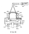
- This fluorine-containing carbon film can be formed by, e.g., a plasma deposition process using the electron cyclotron resonance (ECR). This method will be described below.
- a microwave of 2.45 GHz is first supplied into a plasma producing chamber 801a from a high-frequency power supply part 802 via a waveguide 802a.
- a magnetic field of 875 gausses is applied by magnetic coils 803 and 803a, and Ar gas introduced from an introducing pipe 804 is activated as a high-density plasma by the electron cyclotron resonance.
- C 4 F 8 gas and C 2 H 4 gas are introduced into a deposition chamber 801b from a gas supply part 805 via gas introducing pipes 805a and 805b to be activated by the high-density plasma to form active-species.
- a fluorine-containing carbon film 808 having good adhesion and high hardness is formed on the surface of a wafer 807 which is arranged on a supporting table 806 in the deposition chamber 801b.
- the wafer 807 is fixed by an electrostatic chuck 806a on the supporting table 806.
- the interior of the deposition chamber 801b is evacuated to a predetermined degree of vacuum by an evacuating means (not shown) which is communicated with the deposition chamber 801b via an exhaust pipe 810.
- the fluorine-containing carbon film can be formed.
- a fine patterning process such as the formation of a hole portion for arranging a connecting portion for connecting upper and lower wiring layers to each other.
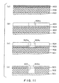
- a fluorine-containing carbon film 902 is formed on a lower wiring layer 901 serving as a substrate as described above.
- an inorganic film 903 of SiO 2 is formed on the fluorine-containing carbon film 902.
- a resist pattern 904 having an opening 904a at a predetermined place is formed on the inorganic film 903 by a well-known photolithography technique.
- the resist pattern 904 is then used as a mask to selectively etch the inorganic film 903.
- a hard mask 905 having an opening 905a at a position corresponding to the opening 904a is formed.
- This etching may be, e.g., a dry etching with the plasma of CF 4 .
- the hard mask 905 is then used as a mask to selectively etch the fluorine-containing carbon film 902.
- a hole portion 906 is formed in the fluorine-containing carbon film 902.
- This etching may be, e.g., a dry etching with the plasma of oxygen gas. If oxygen gas is used, the etch-selectivity (the ratio of etch rates) between the fluorine-containing carbon film 902 and the hard mask 905 can be great. If the plasma of oxygen gas is used, the resist pattern 904 can be simultaneously removed.
- a resist pattern formed by the photolithography technique is generally used as a mask to selectively etch.
- the resist pattern must have an etching resistance as a mask for an underlying layer to be processed.
- the resist pattern must particularly have the etching resistance.
- This resist pattern is formed by, e.g., exposing and developing a photoresist having photosensitivity, and made of an organic material.
- a master pattern of an inorganic material such as SiO 2
- the master pattern is hardly etched with the plasma of oxygen, so that it is possible to carry out a selective etching.
- a hard mask of SiO 2 or the like is used for fine-patterning the fluorine-containing carbon film.
- an inorganic film of SiO 2 or the like is patterned.
- This patterning may use a dry etching with the plasma of CF 4 or C 4 F 8 .
- the resist pattern can be used as a mask to carry out the selective etching to form the hard mask as described above.
- the hard mask since SiO 2 and SiN have low adhesion to the fluorine-containing carbon film which is a fluorine-containing organic film, there is a problem in that the hard mask is easily peeled off.
- the hard mask since the hard mask is made of the insulating material, the hard mask is used as a part of an interlayer dielectric film.
- the fluorine-containing carbon film serving as the interlayer dielectric film is fine-patterned, if a stress is applied in the subsequent process such as forming a metal film for a wiring electrode thereon, the hard mask is sometimes peeled off. If the metal film for the wiring electrode is intended to be flattened by the chemical mechanical polishing method after the metal film is formed, a great stress is applied thereto, so that the hard mask is substantially surely peeled off from the fluorine-containing carbon film.
- the hard mask of SiO 2 or SiN is used for fine-patterning the fluorine-containing carbon film, there is a problem in that the etch-selectivity is lowered as follows. As described above, the dry etching with the plasma of oxygen gas is used for fine-patterning the fluorine-containing carbon film. In view of only this point, a high etch-selectivity should be obtained if the hard mask is made of SiO 2 or SiN.
- the insulating film used as the hard mask is made of a material having a lower relative dielectric constant similar to the insulating film of the fluorine-containing carbon film.
- the present invention has been made in order to eliminate the above described problems. That is, it is an object of the present invention to improve the reliability of a semiconductor device, which has a carbon-containing insulating film, such as a fluorine-containing carbon film, while considering the acceleration of the same.
- a semiconductor device comprising: a semiconductor substrate, on which an active region is formed; a plurality of wiring layers which are formed on the semiconductor substrate; a first insulating layer containing carbon, the first insulating layer being formed at least between any adjacent two of the wiring layers; and a second insulating layer comprising silicon, carbon and nitrogen, the second insulating layer being formed on the first insulating layer.
- the first insulating layer containing carbon contacts the second insulating layer comprising silicon, carbon and nitrogen, so that the adhesion between the first and second insulating layers is improved to inhibit peeling.
- the second insulating layer comprising silicon, carbon and nitrogen can have a higher etch-selectivity than those of conventional layers, and can have a lower dielectric constant than that of an insulating layer comprising silicon and nitrogen or an insulating layer comprising silicon and carbon. Therefore, it is possible to improve the reliability of the semiconductor device while considering the acceleration of the same.
- the second insulating layer preferably further comprises boron in order to lower the relative dielectric constant of the second insulating layer.
- An adhesion layer comprising a high-melting point metal and a nitride thereof may be provided in the interface between the first insulating layer and the wiring layers.
- a method of manufacturing a semiconductor device comprising the steps of: forming a wiring layer on a semiconductor substrate, on which an active region is formed; forming a first insulating layer containing carbon on the wiring layer; forming a second insulating layer comprising silicon, carbon and nitrogen on the first insulating layer; selectively etching the second insulating layer until the surface of the first insulating layer is partially exposed; selectively etching the first insulating layer using the selectively-etched, second insulating layer, as a mask; and forming a new wiring layer on the second insulating layer after selectively etching the first insulating layer.
- the first insulating layer containing carbon contacts the second insulating layer comprising silicon, carbon and nitrogen, between the wiring layers.
- the adhesion between the first and second insulating layers is improved to inhibit peeling.
- the second insulating layer comprising silicon, carbon and nitrogen can have a higher etch-selectivity than those of conventional layers, and can have a lower dielectric constant than that of an insulating layer comprising silicon and nitrogen or an insulating layer comprising silicon and carbon. Therefore, it is possible to improve the reliability of the semiconductor device while considering the acceleration of the same.
- This producing method preferably further comprises a step of adding boron to the second insulating layer in order to lower the relative dielectric constant of the second insulating layer.
- the step of selectively etching the second insulating layer may be carried out with the plasma of the gas of a compound containing carbon and fluorine or with the plasma of the gas of a compound containing carbon and hydrogen.
- the step of selectively etching the first insulating layer is carried out with the plasma of an oxygen-containing gas, the second insulating layer and the wiring layers are hardly etched.
- the step of selectively etching the first insulating layer is carried out with the plasma of a hydrogen-containing gas, the step is controlled by the etching with reactive ions, so that it is possible to carry out a higher anisotropic etching.
- a semiconductor device serving as the first preferred embodiment of the present invention will be described.
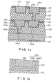
- a semiconductor device is constructed as shown in FIG. 1a.
- An insulating film 101 e.g., an SiO 2 film, is formed so as to cover an active region (not shown), such as a MOS transistor, which is formed on a semiconductor substrate of silicon (Si).
- a wiring layer (not shown) of, e.g., W, which is electrically connected to the active region, and a wiring layer 102 of, e.g., copper (Cu), connected to the wiring layer are formed on the insulating film 101.
- a fluorine-containing carbon film 103 serving as a first insulating film is formed so as to cover the Cu layer 102.
- a groove portion 104a and a hole portion 104b are formed in the fluorine-containing carbon film 103.
- a wiring layer 104 of, e.g., Cu is formed in the groove portion 104a and the hole portion 104b.
- the wiring layer 104 is electrically connected to the Cu layer 102.
- an adhesion layer 104c is formed between the contact surfaces of the Cu layer 104 and the fluorine-containing carbon film 103, and between the contact surface of the Cu layer 104 and the Cu layer 102.
- the adhesion layer 104c comprises, e.g., a TiN layer 104c' and a Ti layer 104c" as shown in FIG. 1b.
- the structure of the adhesion layer 104c should not be limited to such a TiN/Ti stacked structure, but it may be another stacked structure of a high-melting point metal nitride and a high-melting point metal, such as TaN/Ta or WN/W.
- a hard mask 105 of SiCN serving as a second insulating film having a thickness of about 100 nm is formed on the fluorine-containing carbon film 103.
- the SiCN does not always mean a chemical composition or a chemical bonding structure, but it means to include Si, C and N as components.
- a fluorine-containing carbon film 106 serving as a first insulating layer, a Cu layer 107 embedded in a groove portion 107a and a hole portion 107b, an adhesion layer 107c, and a hard mask 108 of SiCN are formed so as to have the same structure as that described above. That is, the hard mask 108 of SiCN is also formed on the fluorine-containing carbon film 106 so as to have a thickness of about 100 nm. Since the Cu layer 104 and the Cu layer 107 are made of the same material, it is not required to form any barrier films on the contact interface therebetween.
- the hard masks 105 and 108 are provided on the interlayer dielectric films 103 and 106 of the fluorine-containing carbon films.
- the hard mask 105 of SiCN is arranged between the fluorine-containing carbon film 103 and the fluorine-containing carbon films 106, so that the adhesion between the respective layers 103, 105 and 106 can be more improved than conventional devices using a hard mask of SiO 2 .
- the same stacked structure may be provided to form a semiconductor device. That is, an optional number of stages of the same stacked structures may be stacked to form a semiconductor device.
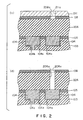
- a fluorine-containing carbon film 206 having a thickness of about 700 nm is formed on the Cu layer 104 and the hard mask 105 of SiCN.
- the fluorine-containing carbon film 206 is formed by a plasma deposition process using the electron cyclotron resonance (ECR) using C 4 F 8 gas and C 2 H 4 gas as raw material gases.
- ECR electron cyclotron resonance
- an insulating film 208 of SiCN is formed on the fluorine-containing carbon film 206.
- This may be formed by the chemical vapor deposition (CVD) method using, e.g., SiH 4 , C 2 H 4 and N 2 as raw material gases.
- CVD chemical vapor deposition
- a resist pattern 211 having a hole portion 211a at a predetermined place is formed on the insulating film 208.
- the resist pattern 211 may be formed by a well-known photolithography technique.
- the resist pattern 211 is then used as a mask to etch the insulating film 208 to form a hard mask 108 having a hole portion 208a as shown in FIG. 2(c).
- This etching may use, e.g., a dry etching with the plasma of C 4 F 8 .
- the hard mask 108 having the hole portion 208a is then used as a mask to etch the underlying fluorine-containing carbon film 206.
- This etching may be a reactive ion etching with the plasma of oxygen gas. Since the hard mask 108 is made of SiCN as described above, the hard mask 108 is hardly etched with the plasma of oxygen gas.
- the fluorine-containing carbon film 206 is etched (ashed) with the plasma of oxygen gas. By this etching process, a hole portion 206a can be formed in the fluorine-containing carbon film 206 as shown in FIG. 2(d). Since the plasma of oxygen gas is used at this time, the resist pattern 211 of the organic film is simultaneously removed.
- the etch rate of SiCN with the plasma of oxygen gas is a far smaller than those of other hard mask materials. Therefore, if the hard mask of SiCN is used as this first preferred embodiment, it is possible to obtain a high etch-selectivity in the etching for the fluorine-containing carbon film, so that it is possible to more improve processing precision.
- a resist pattern 212 having a groove portion 212a is formed on the hard mask 108.
- the resist pattern 212 may be formed by a well-known photolithography technique.
- the groove portion 212a is formed so as to overlap with the hole portion 206a.
- the resist pattern 212 is then used as a mask to etch the hard mask 208 to form a groove 108a in the hard mask 108.
- This etching may be, e.g., a dry etching with the plasma of C 4 F 8 . Since the fluorine-containing carbon film 206 is hardly etched by the dry etching with the plasma C 4 F 8 , the hard mask 108 can be selectively etched.
- the hard mask 108 having the groove portion 108a is then used as a mask to etch the fluorine-containing carbon film 206 to form a fluorine-containing carbon film 106 formed with a groove portion 107a having a depth of about 400 nm as shown in FIG. 2(f).
- a reactive ion etching with the plasma of oxygen gas may be used. Since the plasma of oxygen gas is used, the resist pattern 212 on the hard mask 108 is simultaneously removed.
- a through-hole 107b based on the hole portion 206a, which has been formed in the fluorine-containing carbon film 206, is arranged in a region in which the groove portion 107a of the fluorine-containing carbon film 106 intends to be formed.
- a thin metal film 207a which is an adhesion layer of a TiN layer and a Ti layer, is formed so as to cover the hard mask 108 and the surfaces of the through-hole 107b and groove portions 107a and 108a.
- Ametal film 207 of copper is then formed on the hard mask 108 via the metal film 207a so as to be filled in the through-hole 107b and the groove portions 107a and 108a.
- the metal film 207 may be formed by, e.g., a well-known metal film forming method, such as an electroless plating or a sputtering method.
- the metal films 207 and 207a are then polished from the surface by the chemical mechanical polishing (CMP). If the surface of the hard mask 108 is thus exposed as shown in FIG. 2(h), the Cu layer 107 is arranged on the Cu layer 104 via the fluorine-containing carbon film 106, and the fluorine-containing carbon film 106 and the Cu layer 107 contact each other via the adhesion layer 107c having the TiN/Ti structure.
- CMP chemical mechanical polishing
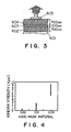
- the adhesive strengths are measured as follows. First, as shown in FIG. 3, a fluorine-containing carbon film 602, a hard mask 603 and a fluorine-containing carbon film 604 are sequentially stacked on a substrate 601 to prepare a sample, and a test rod 605 is fixed to the fluorine-containing carbon film 604 by a predetermined adhesive. A load is then applied to the test rod 605 so that the test rod 605 goes away from the substrate while the substrate 601 is fixed. It is assumed that the adhesive strength is a load (Kpsi) applied when any one of the films is peeled off.
- Kpsi load
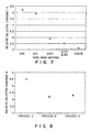
- FIG. 4 The measured results of the above described adhesive strengths are shown in FIG. 4.
- the adhesive strength to the fluorine-containing carbon film is remarkably improved by using SiCN as the material of the hard mask.
- SiCN As the material of the hard mask.
- an adhesive strength of 5 Kpsi or more is thus obtained between the hard mask and the fluorine-containing carbon film, even if the hard mask remains as a part of the interlayer film, the hard mask is inhibited from being peeled off by the chemical mechanical polishing during the formation of the electrode (wiring layer).
- the underlying film A is the above described fluorine-containing carbon film
- the underlying film B is a "SiCO(H) film, where (H) is H in a C x H y group”
- the underlying film C is an SOD (Spin On Dielectric) film.
- the method for measuring the adhesive strength is the same as the above described method.
- the SiCO(H) film is formed by the plasma CVD method using, e.g., methylsilane which is expressed by SiH x (CH 3 ) y , or an alkoxysilane as a raw material, alone or with oxygen-containing gas (O 2 , N 2 O, etc.).
- the SOD film is made of SiLK which is an organic polymer.
- the hard mask is used as a part of an interlayer dielectric film between wiring layers. Therefore, even if the hard mask is thinner than the fluorine-containing carbon film, it is desirable that its dielectric constant is as small as possible. Therefore, comparing the relative dielectric constants ⁇ of various hard mask materials with each other as shown in the graph of FIG. 6, the relative dielectric constant ⁇ of SiCN in this preferred embodiment is about 5.5 which is far lower than about 8 of SiN or SiC although it is higher than about 4 of SiO 2 .
- boron (B) is added to a hard mask of SiCN in order to further lower the dielectric constant of the hard mask material for the above described reason.
- the relative dielectric constant ⁇ of SiCN itself is about 5.5 as described above, the dielectric constant ⁇ can be lowered to about 5.1 if boron is added to SiCN.
- Other constructions are the same as those in the above described first preferred embodiment.
- BF 3 may be used in addition to SiH 4 , C 2 H 4 and N 2 as raw material gases in the chemical vapor deposition method during the formation of the insulating film 208 of SiCN shown in, e.g., FIG. 2(b).
- a combination of raw material gases a combination of SiH 4 , C 2 H 4 and BF 3 , or a combination of SiH 4 , BF 3 and N 2 may be used.
- B 2 F 6 may be used.
- the insulating film is formed of boron-containing SiCN, SiC or SiN (SiBCN, SiBC or SiBN).
- the addition of boron may be carried out by the ion implantation into the insulating film already deposited.
- the hard mask of SiCN has been formed by the process using "SiH 4 + C 2 H 4 + N 2 " as raw material gases in the above described preferred embodiments, the hard mask may be formed by a process using other raw material gases.
- Hard masks of SiCN were formed by different three kinds of processes (raw materials) A, B and C, and the difference between relative dielectric constants of the hard masks of SiCN was examined. The results thereof are shown in the graph of FIG. 8.
- the process A uses "SiH 4 + (a carbon-containing raw material gas) + (a nitrogen-containing raw material gas)" as raw material gases, similar to the above described process.
- SiH 4 in the process A is replaced with SiH x (CH 3 ) y and an alkoxysilane, respectively, to be used as raw material gases.
- the carbon-containing raw material gas may be CH 4 , C 2 H 6 , C 3 H 8 or C 2 H 2 other than the above described C 2 H 4 .
- the nitrogen-containing raw material gas may be NF 3 , N 2 O, NO 2 , N 2 O 4 , NO or NH 4 other than the above described N 2 .
- the relative dielectric constant ⁇ is about 5.5 in the process A which is used in the above described preferred embodiment
- the relative dielectric constants ⁇ in the processes B and C are lowered to be about 4.2 to 4.3. That is, according to the above described processes B and C, the relative dielectric constant can be further lowered as compared with that in the above described second preferred embodiment that boron is added.
- the plasma of oxygen gas has been used for etching the fluorine-containing carbon film
- the plasma of a mixed gas of hydrogen gas, argon gas and nitrogen gas may be used.
- the flow ratio of argon gas to the mixed gas Ar / (N 2 + H 2 + Ar)
- the flow ratio of hydrogen gas to nitrogen gas H 2 / (N 2 + H 2 )
- the degree of vacuum in plasma producing atmosphere may be about 5 mTorr to about 15 mTorr.
- the etch rate (nm/min.) of the hard mask material of SiCN is far smaller than those of other hard mask materials.
- reactive ions and radicals are produced as etching active-species by producing plasma in dry etching processes.
- a reactive ion etching an electric field is utilized for mainly flying reactant ions to an object to be etched, the process is carried out in a high vertical anisotropic state.
- the etching active-species against the fluorine-containing carbon film mainly become reactive hydrogen ions and radicals.
- hydrogen radicals do not have so high reactivity with respect to organic compounds.
- the etching active-species against the fluorine-containing carbon film are substantially only reactive hydrogen ions. That is, in this case, the etching hardly proceeds by radicals having no directionality.
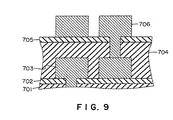
- FIG. 9 a structure shown in FIG. 9 may be provided.
- a hard mask 702 of SiCN is formed on an interlayer dielectric film 701 of a fluorine-containing carbon film, and a wiring layer 703 is formed thereon.
- the wiring layer 703 is connected to an underlying wiring layer (not shown) via a through-hole which is formed in the interlayer dielectric layer 701 and hard mask 702.
- an interlayer dielectric film 704 of a fluorine-containing carbon film is formed so as to cover the wiring layer 703.
- a hard mask 705 of SiCN is formed on the interlayer dielectric film 704, and a wiring layer 706 is formed thereon.
- the wiring layer 706 is connected to an underlying wiring layer 703 via a through-hole which is formed in the interlayer dielectric film 704 and hard mask 705.
- the hard masks 702 and 705 are used for forming the through-holes for connecting the wiring layers to each other. Therefore, in this case, one fine patterning process is carried out for, e.g., the hard mask 705 and the interlayer dielectric film 704.
- the wiring layer 706 is formed by forming a metal film on the hard mask 705 and by fine-patterning the metal film by well-known photolithography and etching techniques.
- the wiring layer has been made of Cu in the above described preferred embodiments, the present invention should not be limited thereto, but the wiring layer may be made of any one of other conductive materials, such as aluminum (Al).
Landscapes
- Internal Circuitry In Semiconductor Integrated Circuit Devices (AREA)
- Drying Of Semiconductors (AREA)
Abstract
Description
| Fluorine-containing carbon film | 1538 |
| SiN | 37 |
| SiC | 45 |
| SiO2 | 42 |
| SiCN | 15 |
| Fluorine-containing carbon film | 1826 |
| SiN | 58 |
| SiC | 88 |
| SiO2 | 95 |
| SiCN | 18 |
Claims (9)
- A semiconductor device comprising:a semiconductor substrate, on which an active region is formed;a plurality of wiring layers which are formed on said semiconductor substrate;a first insulating layer containing carbon, said first insulating layer being formed at least between any adjacent two of said wiring layers; anda second insulating layer comprising silicon, carbon and nitrogen, said second insulating layer being formed on said first insulating layer.
- A semiconductor device as set forth in claim 1, wherein said second insulating layer further comprises boron.
- A semiconductor device as set forth in claim 1 or 2, which further comprises an adhesion layer which comprises a high-melting point metal and a nitride thereof, said adhesion layer being formed in the interface between said first insulating layer and said wiring layers.
- A method of manufacturing a semiconductor device, said method comprising the steps of:forming a wiring layer on a semiconductor substrate, on which an active region is formed;forming a first insulating layer containing carbon on said wiring layer;forming a second insulating layer comprising silicon, carbon and nitrogen on said first insulating layer;selectively etching said second insulating layer until the surface of said first insulating layer is partially exposed;selectively etching said first insulating layer using said selectively-etched second insulating layer as a mask; andforming a new wiring layer on said second insulating layer after selectively etching said first insulating layer.
- A method of manufacturing a semiconductor device as set forth in claim 4, which further comprises a step of adding boron to said second insulating layer.
- A method of manufacturing a semiconductor device as set forth in claim 4 or 5, wherein said step of selectively etching said second insulating layer is carried out with the plasma of the gas of a compound containing carbon and fluorine.
- A method of manufacturing a semiconductor device as set forth in claim 4 or 5, wherein said step of selectively etching said second insulating layer is carried out with the plasma of the gas of a compound containing carbon and hydrogen.
- A method of manufacturing a semiconductor device as set forth in claim 4 or 5, wherein said step of selectively etching said first insulating layer is carried out with the plasma of an oxygen-containing gas.
- A method of manufacturing a semiconductor device as set forth in claim 4 or 5, wherein said step of selectively etching said first insulating layer is carried out with the plasma of a hydrogen-containing gas.
Applications Claiming Priority (3)
| Application Number | Priority Date | Filing Date | Title |
|---|---|---|---|
| JP6238199 | 1999-03-09 | ||
| JP6238199 | 1999-03-09 | ||
| PCT/JP2000/001321 WO2000054329A1 (en) | 1999-03-09 | 2000-03-06 | Semiconductor device and production method therefor |
Publications (3)
| Publication Number | Publication Date |
|---|---|
| EP1146555A1 true EP1146555A1 (en) | 2001-10-17 |
| EP1146555A4 EP1146555A4 (en) | 2004-12-29 |
| EP1146555B1 EP1146555B1 (en) | 2007-12-12 |
Family
ID=13198495
Family Applications (1)
| Application Number | Title | Priority Date | Filing Date |
|---|---|---|---|
| EP00906706A Expired - Lifetime EP1146555B1 (en) | 1999-03-09 | 2000-03-06 | Production method for a semiconductor device |
Country Status (6)
| Country | Link |
|---|---|
| US (2) | US6764939B1 (en) |
| EP (1) | EP1146555B1 (en) |
| KR (1) | KR100407542B1 (en) |
| DE (1) | DE60037395T2 (en) |
| TW (1) | TW483027B (en) |
| WO (1) | WO2000054329A1 (en) |
Cited By (5)
| Publication number | Priority date | Publication date | Assignee | Title |
|---|---|---|---|---|
| WO2002023625A3 (en) * | 2000-09-11 | 2003-03-06 | Tokyo Electron Ltd | Semiconductor device and fabrication method therefor |
| EP1298176A3 (en) * | 2001-09-28 | 2003-10-01 | JSR Corporation | Stacked film insulating film and substrate for semiconductor |
| CN100433294C (en) * | 2004-01-13 | 2008-11-12 | 东京毅力科创株式会社 | Semiconductor device manufacturing method and film formation system |
| EP1898455A4 (en) * | 2005-06-20 | 2009-11-11 | Univ Tohoku | INTERCOULE INSULATING FILM AND CIRCUIT STRUCTURE, AND METHOD FOR PRODUCING THE SAME |
| US20100279510A1 (en) * | 2007-02-09 | 2010-11-04 | Tokyo Electron Limited | Etching method and recording medium |
Families Citing this family (36)
| Publication number | Priority date | Publication date | Assignee | Title |
|---|---|---|---|---|
| US8178435B2 (en) | 1998-12-21 | 2012-05-15 | Megica Corporation | High performance system-on-chip inductor using post passivation process |
| US8421158B2 (en) * | 1998-12-21 | 2013-04-16 | Megica Corporation | Chip structure with a passive device and method for forming the same |
| US6303423B1 (en) | 1998-12-21 | 2001-10-16 | Megic Corporation | Method for forming high performance system-on-chip using post passivation process |
| US8021976B2 (en) | 2002-10-15 | 2011-09-20 | Megica Corporation | Method of wire bonding over active area of a semiconductor circuit |
| US6468956B1 (en) * | 2000-05-24 | 2002-10-22 | Huish Detergents, Inc. | Composition containing α-sulfofatty acid ester and hydrotrope and methods of making and using the same |
| US6429129B1 (en) * | 2000-06-16 | 2002-08-06 | Chartered Semiconductor Manufacturing Ltd. | Method of using silicon rich carbide as a barrier material for fluorinated materials |
| US6759275B1 (en) | 2001-09-04 | 2004-07-06 | Megic Corporation | Method for making high-performance RF integrated circuits |
| JP4015510B2 (en) * | 2002-09-09 | 2007-11-28 | 日本エー・エス・エム株式会社 | Interlayer insulating film for multilayer wiring of semiconductor integrated circuit and manufacturing method thereof |
| US6803660B1 (en) * | 2003-01-29 | 2004-10-12 | International Business Machines Corporation | Patterning layers comprised of spin-on ceramic films |
| US7384727B2 (en) * | 2003-06-26 | 2008-06-10 | Micron Technology, Inc. | Semiconductor processing patterning methods |
| JP4413556B2 (en) * | 2003-08-15 | 2010-02-10 | 東京エレクトロン株式会社 | Film forming method, semiconductor device manufacturing method |
| US7026243B2 (en) * | 2003-10-20 | 2006-04-11 | Micron Technology, Inc. | Methods of forming conductive material silicides by reaction of metal with silicon |
| US6969677B2 (en) * | 2003-10-20 | 2005-11-29 | Micron Technology, Inc. | Methods of forming conductive metal silicides by reaction of metal with silicon |
| JP4715207B2 (en) * | 2004-01-13 | 2011-07-06 | 東京エレクトロン株式会社 | Semiconductor device manufacturing method and film forming system |
| WO2005069367A1 (en) * | 2004-01-13 | 2005-07-28 | Tokyo Electron Limited | Method for manufacturing semiconductor device and film-forming system |
| US7153769B2 (en) * | 2004-04-08 | 2006-12-26 | Micron Technology, Inc. | Methods of forming a reaction product and methods of forming a conductive metal silicide by reaction of metal with silicon |
| US7241705B2 (en) * | 2004-09-01 | 2007-07-10 | Micron Technology, Inc. | Methods of forming conductive contacts to source/drain regions and methods of forming local interconnects |
| US7355282B2 (en) | 2004-09-09 | 2008-04-08 | Megica Corporation | Post passivation interconnection process and structures |
| US8008775B2 (en) | 2004-09-09 | 2011-08-30 | Megica Corporation | Post passivation interconnection structures |
| JP4258518B2 (en) * | 2005-03-09 | 2009-04-30 | 東京エレクトロン株式会社 | Film forming method, film forming apparatus, and storage medium |
| US8384189B2 (en) | 2005-03-29 | 2013-02-26 | Megica Corporation | High performance system-on-chip using post passivation process |
| CN1901162B (en) | 2005-07-22 | 2011-04-20 | 米辑电子股份有限公司 | Method for manufacturing circuit assembly by continuous electroplating and circuit assembly structure |
| KR100724568B1 (en) * | 2005-10-12 | 2007-06-04 | 삼성전자주식회사 | Semiconductor memory device and manufacturing method thereof |
| US20070139855A1 (en) * | 2005-12-21 | 2007-06-21 | Asml Netherlands B.V. | Lithographic apparatus and method of manufacturing an electrostatic clamp for a lithographic apparatus |
| US7851351B2 (en) | 2006-03-31 | 2010-12-14 | Tokyo Electron Limited | Manufacturing method for semiconductor devices with enhanced adhesivity and barrier properties |
| JP5119606B2 (en) * | 2006-03-31 | 2013-01-16 | 東京エレクトロン株式会社 | Semiconductor device and manufacturing method of semiconductor device |
| JP5194393B2 (en) * | 2006-06-23 | 2013-05-08 | 東京エレクトロン株式会社 | Manufacturing method of semiconductor device |
| KR100731496B1 (en) * | 2006-08-31 | 2007-06-21 | 동부일렉트로닉스 주식회사 | Semiconductor device and manufacturing method |
| JP4929932B2 (en) * | 2006-09-01 | 2012-05-09 | 東京エレクトロン株式会社 | Film forming method, film forming apparatus, and storage medium |
| US8021975B2 (en) * | 2007-07-24 | 2011-09-20 | Tokyo Electron Limited | Plasma processing method for forming a film and an electronic component manufactured by the method |
| US8197913B2 (en) * | 2007-07-25 | 2012-06-12 | Tokyo Electron Limited | Film forming method for a semiconductor |
| JP2010171064A (en) * | 2009-01-20 | 2010-08-05 | Panasonic Corp | Semiconductor device and method of manufacturing same |
| CN109494192B (en) | 2017-09-11 | 2020-10-09 | 联华电子股份有限公司 | Semiconductor element and manufacturing method thereof |
| JP2021082703A (en) | 2019-11-19 | 2021-05-27 | キオクシア株式会社 | Semiconductor device and method for manufacturing the same |
| US12108593B2 (en) * | 2021-12-06 | 2024-10-01 | Changxin Memory Technologies, Inc. | Method for preparing semiconductor structure using a first mask comprises a groove |
| US12564022B2 (en) * | 2022-07-11 | 2026-02-24 | Applied Materials, Inc. | Carbon hardmask opening using boron nitride mask |
Family Cites Families (14)
| Publication number | Priority date | Publication date | Assignee | Title |
|---|---|---|---|---|
| US4244799A (en) * | 1978-09-11 | 1981-01-13 | Bell Telephone Laboratories, Incorporated | Fabrication of integrated circuits utilizing thick high-resolution patterns |
| JPH0992616A (en) * | 1995-07-18 | 1997-04-04 | Canon Inc | Membrane and mask, exposure apparatus and device manufacturing method using the same |
| JP3323055B2 (en) * | 1996-04-03 | 2002-09-09 | 株式会社東芝 | Semiconductor device and manufacturing method thereof |
| JP3409984B2 (en) * | 1996-11-14 | 2003-05-26 | 東京エレクトロン株式会社 | Semiconductor device and method of manufacturing semiconductor device |
| JP3400918B2 (en) * | 1996-11-14 | 2003-04-28 | 東京エレクトロン株式会社 | Method for manufacturing semiconductor device |
| US6100184A (en) * | 1997-08-20 | 2000-08-08 | Sematech, Inc. | Method of making a dual damascene interconnect structure using low dielectric constant material for an inter-level dielectric layer |
| TW368741B (en) * | 1998-02-26 | 1999-09-01 | United Microelectronics Corp | Manufacturing method for dual damascene |
| US6077789A (en) * | 1998-07-14 | 2000-06-20 | United Microelectronics Corp. | Method for forming a passivation layer with planarization |
| JP3148183B2 (en) * | 1998-08-31 | 2001-03-19 | 日本電気株式会社 | Method for manufacturing semiconductor device |
| US6251802B1 (en) * | 1998-10-19 | 2001-06-26 | Micron Technology, Inc. | Methods of forming carbon-containing layers |
| US6211068B1 (en) * | 1999-05-25 | 2001-04-03 | United Microelectronics Corp. | Dual damascene process for manufacturing interconnects |
| US6593653B2 (en) * | 1999-09-30 | 2003-07-15 | Novellus Systems, Inc. | Low leakage current silicon carbonitride prepared using methane, ammonia and silane for copper diffusion barrier, etchstop and passivation applications |
| US6211061B1 (en) * | 1999-10-29 | 2001-04-03 | Taiwan Semiconductor Manufactuirng Company | Dual damascene process for carbon-based low-K materials |
| US6774489B2 (en) * | 2000-08-29 | 2004-08-10 | Texas Instruments Incorporated | Dielectric layer liner for an integrated circuit structure |
-
2000
- 2000-03-06 DE DE60037395T patent/DE60037395T2/en not_active Expired - Lifetime
- 2000-03-06 EP EP00906706A patent/EP1146555B1/en not_active Expired - Lifetime
- 2000-03-06 KR KR10-2001-7010379A patent/KR100407542B1/en not_active Expired - Fee Related
- 2000-03-06 WO PCT/JP2000/001321 patent/WO2000054329A1/en not_active Ceased
- 2000-03-08 TW TW089104183A patent/TW483027B/en not_active IP Right Cessation
- 2000-09-08 US US09/658,861 patent/US6764939B1/en not_active Expired - Fee Related
-
2004
- 2004-05-24 US US10/851,200 patent/US20040219736A1/en not_active Abandoned
Cited By (11)
| Publication number | Priority date | Publication date | Assignee | Title |
|---|---|---|---|---|
| WO2002023625A3 (en) * | 2000-09-11 | 2003-03-06 | Tokyo Electron Ltd | Semiconductor device and fabrication method therefor |
| US6949829B2 (en) * | 2000-09-11 | 2005-09-27 | Tokyo Electron Limited | Semiconductor device and fabrication method therefor |
| EP1777739A3 (en) * | 2000-09-11 | 2008-09-17 | Tokyo Electron Limited | Semiconductor device and fabrication method therefor |
| EP1298176A3 (en) * | 2001-09-28 | 2003-10-01 | JSR Corporation | Stacked film insulating film and substrate for semiconductor |
| US6824833B2 (en) | 2001-09-28 | 2004-11-30 | Jsr Corporation | Stacked film, insulating film and substrate for semiconductor |
| CN100433294C (en) * | 2004-01-13 | 2008-11-12 | 东京毅力科创株式会社 | Semiconductor device manufacturing method and film formation system |
| EP1898455A4 (en) * | 2005-06-20 | 2009-11-11 | Univ Tohoku | INTERCOULE INSULATING FILM AND CIRCUIT STRUCTURE, AND METHOD FOR PRODUCING THE SAME |
| US8193642B2 (en) | 2005-06-20 | 2012-06-05 | Tohoku University | Interlayer insulating film, interconnection structure, and methods of manufacturing the same |
| TWI402964B (en) * | 2005-06-20 | 2013-07-21 | 國立大學法人 東北大學 | Interlayer insulating film and wiring structure and manufacturing method therefor |
| US20100279510A1 (en) * | 2007-02-09 | 2010-11-04 | Tokyo Electron Limited | Etching method and recording medium |
| US8383519B2 (en) * | 2007-02-09 | 2013-02-26 | Tokyo Electron Limited | Etching method and recording medium |
Also Published As
| Publication number | Publication date |
|---|---|
| KR100407542B1 (en) | 2003-11-28 |
| EP1146555B1 (en) | 2007-12-12 |
| KR20020002390A (en) | 2002-01-09 |
| DE60037395T2 (en) | 2008-11-27 |
| EP1146555A4 (en) | 2004-12-29 |
| WO2000054329A1 (en) | 2000-09-14 |
| DE60037395D1 (en) | 2008-01-24 |
| US20040219736A1 (en) | 2004-11-04 |
| TW483027B (en) | 2002-04-11 |
| US6764939B1 (en) | 2004-07-20 |
Similar Documents
| Publication | Publication Date | Title |
|---|---|---|
| EP1146555B1 (en) | Production method for a semiconductor device | |
| US6417092B1 (en) | Low dielectric constant etch stop films | |
| US7811926B2 (en) | Multilayer hardmask scheme for damage-free dual damascene processing of SiCOH dielectrics | |
| KR100878170B1 (en) | Dual Frequency Plasma Chemical Vapor Deposition of Silicon Carbide Layers | |
| US7144606B2 (en) | Plasma treatment to enhance adhesion and to minimize oxidation of carbon-containing layers | |
| US6380096B2 (en) | In-situ integrated oxide etch process particularly useful for copper dual damascene | |
| US7132369B2 (en) | Method of forming a low-K dual damascene interconnect structure | |
| US6855484B2 (en) | Method of depositing low dielectric constant silicon carbide layers | |
| US20030119307A1 (en) | Method of forming a dual damascene structure | |
| US20030027427A1 (en) | Integrated system for oxide etching and metal liner deposition | |
| US20050009320A1 (en) | Method of forming silicon carbide films | |
| US6972453B2 (en) | Method of manufacturing a semiconductor device capable of etching a multi-layer of organic films at a high selectivity | |
| EP1186685A2 (en) | Method for forming silicon carbide films | |
| US7014887B1 (en) | Sequential sputter and reactive precleans of vias and contacts | |
| US6727182B2 (en) | Process for the production of semiconductor device | |
| US6620739B1 (en) | Method of manufacturing semiconductor device | |
| US7091612B2 (en) | Dual damascene structure and method | |
| JP4260764B2 (en) | Manufacturing method of semiconductor device | |
| KR100670618B1 (en) | Sequential Sputtering and Reactive Precleaning of Vias and Contacts | |
| US20020001950A1 (en) | Method of manufacturing copper wiring in a semiconductor device | |
| US20060166491A1 (en) | Dual damascene interconnection having low k layer and cap layer formed in a common PECVD process | |
| KR100367852B1 (en) | Method for Etching With High Selectivity To Photoresist | |
| JPWO2000054329A1 (en) | Semiconductor device and manufacturing method thereof |
Legal Events
| Date | Code | Title | Description |
|---|---|---|---|
| PUAI | Public reference made under article 153(3) epc to a published international application that has entered the european phase |
Free format text: ORIGINAL CODE: 0009012 |
|
| 17P | Request for examination filed |
Effective date: 20010717 |
|
| AK | Designated contracting states |
Kind code of ref document: A1 Designated state(s): AT BE CH CY DE DK ES FI FR GB GR IE IT LI LU MC NL PT SE |
|
| RBV | Designated contracting states (corrected) |
Designated state(s): BE DE FR GB IT NL |
|
| A4 | Supplementary search report drawn up and despatched |
Effective date: 20041116 |
|
| 17Q | First examination report despatched |
Effective date: 20060816 |
|
| RTI1 | Title (correction) |
Free format text: PRODUCTION METHOD FOR A SEMICONDUCTOR DEVICE |
|
| GRAP | Despatch of communication of intention to grant a patent |
Free format text: ORIGINAL CODE: EPIDOSNIGR1 |
|
| GRAS | Grant fee paid |
Free format text: ORIGINAL CODE: EPIDOSNIGR3 |
|
| GRAA | (expected) grant |
Free format text: ORIGINAL CODE: 0009210 |
|
| AK | Designated contracting states |
Kind code of ref document: B1 Designated state(s): BE DE FR GB IT NL |
|
| REG | Reference to a national code |
Ref country code: GB Ref legal event code: FG4D |
|
| REF | Corresponds to: |
Ref document number: 60037395 Country of ref document: DE Date of ref document: 20080124 Kind code of ref document: P |
|
| PG25 | Lapsed in a contracting state [announced via postgrant information from national office to epo] |
Ref country code: NL Free format text: LAPSE BECAUSE OF FAILURE TO SUBMIT A TRANSLATION OF THE DESCRIPTION OR TO PAY THE FEE WITHIN THE PRESCRIBED TIME-LIMIT Effective date: 20071212 |
|
| NLV1 | Nl: lapsed or annulled due to failure to fulfill the requirements of art. 29p and 29m of the patents act | ||
| PG25 | Lapsed in a contracting state [announced via postgrant information from national office to epo] |
Ref country code: BE Free format text: LAPSE BECAUSE OF FAILURE TO SUBMIT A TRANSLATION OF THE DESCRIPTION OR TO PAY THE FEE WITHIN THE PRESCRIBED TIME-LIMIT Effective date: 20071212 |
|
| EN | Fr: translation not filed | ||
| PLBE | No opposition filed within time limit |
Free format text: ORIGINAL CODE: 0009261 |
|
| STAA | Information on the status of an ep patent application or granted ep patent |
Free format text: STATUS: NO OPPOSITION FILED WITHIN TIME LIMIT |
|
| PG25 | Lapsed in a contracting state [announced via postgrant information from national office to epo] |
Ref country code: FR Free format text: LAPSE BECAUSE OF FAILURE TO SUBMIT A TRANSLATION OF THE DESCRIPTION OR TO PAY THE FEE WITHIN THE PRESCRIBED TIME-LIMIT Effective date: 20080926 |
|
| 26N | No opposition filed |
Effective date: 20080915 |
|
| GBPC | Gb: european patent ceased through non-payment of renewal fee |
Effective date: 20080312 |
|
| PG25 | Lapsed in a contracting state [announced via postgrant information from national office to epo] |
Ref country code: GB Free format text: LAPSE BECAUSE OF NON-PAYMENT OF DUE FEES Effective date: 20080312 |
|
| PG25 | Lapsed in a contracting state [announced via postgrant information from national office to epo] |
Ref country code: IT Free format text: LAPSE BECAUSE OF NON-PAYMENT OF DUE FEES Effective date: 20080331 |
|
| PGFP | Annual fee paid to national office [announced via postgrant information from national office to epo] |
Ref country code: DE Payment date: 20120404 Year of fee payment: 13 |
|
| REG | Reference to a national code |
Ref country code: DE Ref legal event code: R119 Ref document number: 60037395 Country of ref document: DE Effective date: 20131001 |
|
| PG25 | Lapsed in a contracting state [announced via postgrant information from national office to epo] |
Ref country code: DE Free format text: LAPSE BECAUSE OF NON-PAYMENT OF DUE FEES Effective date: 20131001 |