EP1146489A2 - Sensoreinrichtung und Verfahren zum berührungslosen Abtasten einer Oberfläche eines Gegenstandes - Google Patents
Sensoreinrichtung und Verfahren zum berührungslosen Abtasten einer Oberfläche eines Gegenstandes Download PDFInfo
- Publication number
- EP1146489A2 EP1146489A2 EP01108145A EP01108145A EP1146489A2 EP 1146489 A2 EP1146489 A2 EP 1146489A2 EP 01108145 A EP01108145 A EP 01108145A EP 01108145 A EP01108145 A EP 01108145A EP 1146489 A2 EP1146489 A2 EP 1146489A2
- Authority
- EP
- European Patent Office
- Prior art keywords
- sensor
- sensor elements
- elements
- coin
- individual
- Prior art date
- Legal status (The legal status is an assumption and is not a legal conclusion. Google has not performed a legal analysis and makes no representation as to the accuracy of the status listed.)
- Granted
Links
- 238000000034 method Methods 0.000 title claims abstract description 39
- 239000011159 matrix material Substances 0.000 claims abstract description 27
- 230000001939 inductive effect Effects 0.000 claims description 5
- 230000003287 optical effect Effects 0.000 claims description 2
- 230000000704 physical effect Effects 0.000 claims 2
- 238000012360 testing method Methods 0.000 description 9
- 238000011161 development Methods 0.000 description 5
- 238000004364 calculation method Methods 0.000 description 2
- 238000010276 construction Methods 0.000 description 2
- 230000005693 optoelectronics Effects 0.000 description 2
- 238000010200 validation analysis Methods 0.000 description 2
- 230000004304 visual acuity Effects 0.000 description 2
- 238000013461 design Methods 0.000 description 1
- 238000001514 detection method Methods 0.000 description 1
- 238000004049 embossing Methods 0.000 description 1
- 230000006870 function Effects 0.000 description 1
- 238000007689 inspection Methods 0.000 description 1
- 230000010354 integration Effects 0.000 description 1
- 238000004519 manufacturing process Methods 0.000 description 1
- 239000000463 material Substances 0.000 description 1
- 239000000523 sample Substances 0.000 description 1
- 230000003595 spectral effect Effects 0.000 description 1
- 238000012795 verification Methods 0.000 description 1
Images


Classifications
-
- G—PHYSICS
- G07—CHECKING-DEVICES
- G07D—HANDLING OF COINS OR VALUABLE PAPERS, e.g. TESTING, SORTING BY DENOMINATIONS, COUNTING, DISPENSING, CHANGING OR DEPOSITING
- G07D5/00—Testing specially adapted to determine the identity or genuineness of coins, e.g. for segregating coins which are unacceptable or alien to a currency
- G07D5/005—Testing the surface pattern, e.g. relief
Definitions
- the invention is in the field of contactless scanning of surfaces of objects especially of coins, coin-like tokens or similar items.
- Methods for contactless checking of coins are made more inductive, for example and / or opto-electronic means performed.
- a method is known from the document EP 0508560 and a device for contactless checking of coins is known.
- the authenticity of the coin is checked using sampled physical signals. During the test, the coin is rotated by at least 360 ° within a test cycle, the coin initially with the aid of radially adjustable clamping elements compared to a sensor centered and then rotated.
- coin verification is that accurate and exact detection and centering of the coin to be checked takes place since even the smallest inaccuracies and deviations during centering and subsequent scanning for misinterpretations and operational disturbances being able to lead. This is a relatively large mechanical in the known method Effort necessary.
- the invention is therefore based on the object of a sensor device and a method for contactless scanning of a surface of objects, in particular a coin, one to create coin-like token or similar items that allow the mechanical effort to achieve sufficient accuracy in coin validation reduce, the sensor device and the method should be designed so that surfaces various objects can be scanned.
- a sensor device solved in that the sensor has several sensor elements with a respective individual Has sensor surface, the individual sensor surfaces of the plurality of sensor elements a sensor matrix is formed, and the plurality of sensor elements for non-contact Scanning can be addressed individually in such a way that a number is formed from the plurality of sensor elements selected sensor elements can be electronically selected and addressed.
- the main advantage which the invention achieves over the prior art is is that a way is created, a coin or some other object that is arranged opposite the sensor device in different surface areas to scan by selecting sensor elements individually. This allows for any trained coins or objects are scanned signals in different surface areas are processed and used to identify the coin or item.
- the Sensor device is fundamentally for every kind of coins, coin-like tokens or objects suitable without having to make any design changes to the Adapt sensor device for scanning certain objects. The adjustment to Different coins or objects are scanned in particular by certain ones Sensor elements for scanning can be individually addressed. This is one for the most varied Applications suitable sensor device created.
- the test accuracy of the scanning process can be optimized in that the one to be tested Coin and the scanning device (sensor device) during the scanning process relative to one another are in a rest position. However, it can also be provided that the coin to be checked or the object to be tested moves relative to the scanning device during the scanning process when the test accuracy achieved in such a scanning process for the particular Use case is sufficient.
- An expedient development of the invention provides that the multiple sensor elements are so are arranged so that the number of selected sensor elements can be selected so that the essentially along the respective individual sensor surfaces of the selected sensor elements a circular path are arranged. As a result, the selected sensor elements are along a simple, closed, geometric curve arranged.
- the distances between adjacent ones of the several sensor elements are expediently small Dimensions of the respective individual sensor surface of the neighboring sensor elements, which enables a fine scanning grid for coin validation.
- part of the plurality Sensor elements is arranged along at least two lines. With the help of along the Signals detected on both lines can advantageously have dimensions of the object to be tested determined or used for further calculations.
- Calculations on the relative location of the surface of the object to be scanned with respect to the Sensor devices can advantageously be implemented when using the at least two Lines an axis cross is formed.
- a development of the invention provides that sensor elements that run along the at least two lines are arranged, each designed as a lens sensor element.
- the time for scanning along a curve running on the coin to be tested can be minimized be, if it is provided according to an advantageous embodiment of the invention that the Several sensor elements Sensor elements with an individual, at least partially revolving Include sensor surface, the at least partially circumferential, individual sensor surface each at least partially surrounds an inner opening.
- the comparison of the sampled signals with existing standard signals can then be carried out if the at least partially circumferential, individual sensor surface essentially is formed along a circular path, the radii of the respective circular paths differentiate.
- the at least partially encircling, individual sensor surface of one of the sensor elements, the at least partially encircling, individual sensor surface of another of the sensor elements at least partially includes.
- An unaffected by electromagnetic interference and the scanning of surface features the coin to be checked or the item to be checked is then a comprehensive check expediently executable if the plurality of sensor elements comprise optical sensor elements.
- a light source for illuminating the surface of the object is arranged.
- a further development of the invention provides that the multiple sensor elements are inductive and / or include magneto-optical sensor elements, which additionally material properties of the checking coin can be detected.
- an electrical coil can expediently be located in the area of the sensor matrix be arranged.
- One with regard to optimizing the density of individual sensor areas per partial area of the Sensor matrix and a convenient electronic circuit of the sensor device provides that one or all of the multiple sensor elements are integrated on one Electronic component are formed, which is included in the sensor.
- a preferred development of the invention provides that one or all of the plurality of sensor elements are formed as bonded components, which makes it simple, with little effort Realizable construction of the sensor device is made possible.
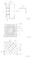
- a coin 1 for checking a sensor device 2 is arranged opposite one another.
- the coin 1 is scanned with the aid of several sensor elements of the sensor device 2. This is shown schematically in FIG. 1 with the aid of arrows A.
- To scan the coin 1 includes the sensor device 2 a plurality of sensor elements (not shown in FIG. 1), each one have individual sensor surface. The individual sensor areas form a sensor matrix 3, facing the coin 1.
- the multiple sensor elements are used to scan the coin 1 the sensor device 2 with the aid of a control device 4, which is electrical with the sensor device is individually addressed so that for selected sensor elements of the plurality Sensor elements of the sensor device 2 each trigger a scanning process and the scanning signals detected here by means of the control device 4 from the selected sensor elements can be read out.
- the multiple sensor elements individually or in Groups can be addressed simultaneously or in succession.
- the read scanning signals or characteristic values derived from this are then compared with previously stored standard signals, to decide whether the coin 1 is of a certain coin type.
- the standard signals are stored in memory means of the control device 4.
- the control facility 4 it can be any electronic device that is suitable for the plurality To address and control sensor elements of sensor device 2 individually and separately and / or read out. It can be provided that the control device 4 also the voltage supply controls the sensor device 2.
- control device can perform 4 further control functions in a coin checking device (not shown) in which the sensor device 2 and the control device 4 are arranged are take over.
- a coin checking device (not shown) in which the sensor device 2 and the control device 4 are arranged are take over.
- the control device 4 depending on Result of the coin check a process for sorting coins that are controlled as falsely recognized.
- the control device 4 can be fully or partially integrated into the sensor device 2.
- the object to be checked with the aid of the sensor device 2 was used in connection with FIG. 1 referred to as a coin 1.
- the item to be checked can also be coin-like tokens, tokens or any, especially flat objects, for example Act buttons, their dimensions to the sensor matrix 3 of the sensor device 2 in one are such a size ratio that scanning signals are detected with the aid of the sensor device that can be used to identify the item.
- a sensor device 20 is shown in front view in FIG.
- a sensor matrix 22 is formed from individual sensor surfaces 21 of the sensor elements.
- the individual Sensor surfaces 21 are arranged in rows and columns.
- the sensor elements of the sensor device 20 can be selected such that the individual sensor surfaces 21 of the selected sensor elements along any curve shape are arranged. In FIG. 2 this is an example of those lying on a circular path 23 individual sensor surfaces 21 shown.
- the sensor device 20 can be implemented any curve shape due to the grid-like Arrangement of the individual sensor surfaces 21 is possible.
- the along the desired curve arranged and selected sensor elements preferably simultaneously addressed so that the scanning process for checking the coin is carried out in the shortest possible time can be. How many sensor elements can be addressed or read out simultaneously depends essentially on the capacity or performance of the sensor device 20 connected control device.
- a further sensor device 30 is shown schematically in front view. Compared 2 are arranged in adjacent rows 31, 32 to the sensor device 20 according to FIG individual sensor surfaces 33 offset from one another. With the help of such an arrangement of the individual sensor surfaces 33 it is possible, for example, to select sensor elements in such a way that their individual sensor surfaces 34 lie along a square curve 35.
- FIG. 4 schematically shows a sensor device 40 in which the multiple sensors, whose individual sensor surfaces 41 form a sensor matrix 42, of a different type are.
- the multiple sensors whose individual sensor surfaces 41 form a sensor matrix 42, of a different type are.
- one part 43 of the several sensor elements, as shown in FIG. 4 is arranged such that an axis cross 45 is formed.
- a center can then be created with the aid of one part 43 of the plurality of sensor elements of the coin to be checked can then be determined depending on the determined
- the center of the coin to be tested selected sensor elements for scanning the one to be tested To select a coin. This can ensure, for example, that when scanning the coin to be tested along a circular path the circular path with regard to the coin to be tested is centered. But also any relative positioning with the help of the selected sensor elements realized scan curve with regard to the center of the coin is possible.
- an axis cross 51 can be made using several Sensor elements can be realized that have individual line sensor surfaces 52.
- a sensor device 60 can comprise sensor elements that have a have at least partially circumferential, individual sensor surface 61.
- the at least partially circumferential, individual sensor surfaces 61 can differ with respect to a respective radius distinguish so that the coin to be checked is scanned along several tracks may differ in their respective scope.
- the sensor device 60 can have the at least one partially encircling, individual sensor surfaces include 61 further sensor elements, the closed, have individual sensor surfaces 62. Any combination of sensor elements with line sensor surfaces 52 (see FIG. 5) and / or sensor elements with at least partially circumferential, individual sensor surfaces 61 (see FIG. 6) and / or sensor elements closed, essentially punctiform sensor surfaces 62 are possible.
- This can a sensor device can be individually designed so that it can be used to scan certain coins or flat objects is adapted. It is essential here that the combined Sensor elements can be addressed or read out individually at the same time or one after the other are in order to determine the specific nature of the object to be examined and the the time required to carry out the testing process optimized scanning process.
- a sensor matrix is formed in each case, which is essentially rectangular a sensor matrix can also be provided, which is circular or diamond-shaped or one corresponds to any other geometric shape.
- the sensor device has so far been independent of the individual characteristics of the several Sensor elements described.
- the multiple sensor elements can be optically sensitive, for example Have sensor surfaces (CCD elements, photodiodes).
- CCD elements CCD elements, photodiodes
- the light source for illuminating the coin to be checked can even in the sensor device may be integrated, preferably in the area of the sensor matrix 22 or 42, or are on the edge of the sensor device or the sensor matrix 22 or 42, so that lighting the surface to be scanned is made possible.
- the light source and the optically sensitive Sensor areas are matched to each other with regard to the spectral range used.
- Inductive sensor elements can also be provided.
- the scanning of the Passive coin to be tested using an external magnetic field of a suitable one Frequency or active by the sensor elements of the sensor device for generating Eddy currents create a magnetic field inside or on the surface of the coin to be tested.
- the resulting and sampled signals are then used to obtain features evaluated.
- Means for generating the external magnetic field e.g. coils
- Light source already described can be integrated into the sensor device, preferably in the area of the sensor or the sensor matrix 22 or 42.
- magneto-optical sensor elements can be provided.
- the coin or the flat object relative to the sensor device is moved. For example, between two scans, each of which Sensor elements are individually addressed or read out, that the position the coin or the flat object is changed relative to the sensor device. While of the scanning processes, the coin or the flat object is then at rest relative to the sensor device.
- the accuracy of the surface scanning is fundamentally determined using the sensor device 2 then be executable with the highest accuracy if the coin to be checked or the one to be checked Object during the scanning process in relative calm with respect to the sensor device 2 located.
- the object to be tested is on the sensor device during the scanning process 2 moved over.
- a possibly reduced scanning accuracy can however, certain applications may be sufficient.
- Advantage of one on the sensor device 2 an object moving past during the scanning process would be that a larger one Number of objects can be scanned in a certain time interval since stopping of the object to be checked compared to the sensor device 2 is omitted.
Landscapes
- Physics & Mathematics (AREA)
- General Physics & Mathematics (AREA)
- Testing Of Coins (AREA)
- Image Input (AREA)
Abstract
Description
- Figur 1
- eine schematische Darstellung einer Einrichtung zum Prüfen einer Münze;
- Figur 2
- eine schematische Darstellung einer Sensorfläche mit mehreren Sensorelementen;
- Figur 3
- eine weitere Sensorfläche mit mehreren Sensorelementen;
- Figur 4
- die Sensorfläche nach Figur 2, wobei ein Teil der mehreren Sensorelemente ein höheres Auflösungsvermögen als ein anderer Teil der mehreren Sensorelemente aufweist;
- Figur 5
- eine weitere Ausführungsform einer Sensorfläche, wobei mit Hilfe mehrerer Liniensensorelemente ein Achsenkreuz gebildet ist; und
- Figur 6
- eine andere Ausführungsform einer Sensorfläche, wobei mehrere Sensorelemente eine umlaufende individuelle Sensorfläche aufweisen.
Claims (29)
- Sensoreinrichtung zum berührungslosen Abtasten einer Oberfläche eines Gegenstandes, inbesondere einer Münze, einer münzartigen Wertmarke oder dergleichen, mit einem Sensor, dadurch gekennzeichnet, daß der Sensor mehrere Sensorelemente mit einer jeweiligen individuellen Sensorfläche (21) der aufweist, wobei von den individuellen Sensorflächen (21) der mehreren Sensorelemente eine Sensormatrix (22) gebildet ist, und die mehreren Sensorelemente zum berührungslosen Abtasten einzeln derart adressierbar sind, daß aus den mehreren Sensorelementen eine Anzahl ausgewählter Sensorelemente elektronisch ausgewählt und adressiert werden kann.
- Sensoreinrichtung nach Anspruch 1, dadurch gekennzeichnet, daß die mehreren Sensorelemente so angeordnet sind, daß die Anzahl ausgewählter Sensorelemente ausgewählt werden kann, so daß die jeweiligen individuellen Sensorflächen (21) der ausgewählten Sensorelemente im wesentlichen entlang einer Kreisbahn (23) angeordnet sind.
- Sensoreinrichtung nach Anspruch 1 oder 2, dadurch gekennzeichnet, daß die mehreren Sensorelemente in Reihen und in Spalten angeordnet sind.
- Sensoreinrichtung nach einem der vorangehenden Ansprüche, dadurch gekennzeichnet, daß Abstände zwischen benachbarten der mehreren Sensorelemente klein gegenüber Abmessungen der jeweiligen individuellen Sensorfläche (21) der benachbarten Sensorelemente sind.
- Sensoreinrichtung nach einem der vorangehenden Ansprüche, dadurch gekennzeichnet, daß ein Auflösungsvermögen in einem Bereich der Sensormatrix (22) von einem Auflösungsvermögen in einem anderen Bereich der Sensormatrix (22) verschieden ist.
- Sensoreinrichtung nach einem der vorangehenden Ansprüch, dadurch gekennzeichnet, daß ein Teil der mehreren Sensorelemente entlang mindestens zweier Linien angeordnet ist.
- Sensoreinrichtung nach Anspruch 6, dadurch gekennzeichnet, daß mit Hilfe der mindestens zwei Linien ein Achsenkreuz gebildet ist.
- Sensoreinrichtung nach Anspruch 6 oder 7, dadurch gekennzeichnet, daß Sensorelemente, die entlang der mindestens zwei Linien angeordnet sind, jeweils als Liniensensorelemente (52) augebildet sind.
- Sensoreinrichtung nach einem der vorangehenden Ansprüche, dadurch gekennzeichnet, daß die mehreren Sensorelemente Sensorelemente mit einer wenigstens teilweise umlaufenden, individuellen Sensorfläche (61) umfassen, wobei die wenigstens teilweise umlaufende, individuelle Sensorfläche (61) jeweils eine innere Öffnung zumindest teilweise umgibt.
- Sensoreinrichtung nach Anspruch 9, dadurch gekennzeichnet, daß die wenigstens teilweise umlaufende, individuelle Sensorfläche (61) im wesentlichen entlang einer Kreisbahn ausgebildet ist, wobei sich Radien der jeweiligen Kreisbahnen unterscheiden.
- Sensoreinrichtung nach Anspruch 9 oder 10, dadurch gekennzeichnet, daß die wenigstens teilweise umlaufende, individuelle Sensorfläche eines der Sensorelemente die wenigstens teilweise umlaufende, individuelle Sensorfläche eines anderen der Sensorelement zumindest teilweise umfaßt.
- Sensoreinrichtung nach einem der vorangehenden Ansprüche, dadurch gekennzeichnet, daß die mehreren Sensorelemente optische Sensorelemente umfassen.
- Sensoreinrichtung nach Anspruch 12, dadurch gekennzeichnet, daß im Bereich der Sensormatrix (22) eine Lichtquelle zur Beleuchtung der Oberfläche des Gegenstands angeordnet ist.
- Sensoreinrichtung nach einem der vorangehenden Ansprüche, dadurch gekennzeichnet, daß die mehreren Sensorelemente induktive Sensorelemente umfassen.
- Sensoreinrichtung nach einem der vorangehenden Ansprüche, dadurch gekennzeichnet, daß die mehreren Sensorelemente magneto-optische Sensorelemente umfassen.
- Sensoreinrichtung nach einem der vorangehenden Ansprüche, dadurch gekennzeichnet, daß im Bereich der Sensormatrix (22) eine elektrische Spule angeordnet ist.
- Sensoreinrichtung nach einem der vorangehenden Ansprüche, dadurch gekennzeichnet, daß ein oder alle der mehreren Sensorelemente auf einem integrierten elektronischen Bauelement ausgebildet sind, welches von dem Sensor umfaßt ist.
- Sensoreinrichtung nach einem der vorangehenden Ansprüche, dadurch gekennzeichnet, daß ein oder alle der mehreren Sensorelemente als gebondete Bauelemente ausgebildet sind.
- Verfahren zum berührungslosen Abtasten einer Oberfläche eines Gegenstands, insbesondere einer Münze, einer münzartigen Wertmarke oder dergleichen mit Hilfe einer einen Sensor aufweisenden Sensoreinrichtung, wobei der Sensor mehrere Sensorelemente mit einer jeweiligen individuellen Sensorfläche (21) aufweist und die mehreren Sensorelemente eine Sensormatrix (22) bilden, das Verfahren die folgenden Schritte aufweisend:a) Positionieren des Gegenstands gegenüber der Sensormatrix (22);b) elektronisches Auswählen einer Anzahl ausgewählter Sensorelemente;c) individuelles, elektronisches Adressieren der ausgewählten Sensorelemente, um zumindest eine physikalische Eigenschaft des flächigen Gegenstands abzutasten; undd) Auswerten der zumindest einen abgetasteten physikalischen Eigenschaft des flächigen Gegenstands.
- Verfahren nach Anspruch 19, dadurch gekennzeichnet, daß die ausgewählten Sensorelemente beim individuellen, elektronischen adressieren gemäß Verfahrensschritt c) parallel adressiert werden.
- Verfahren nach Anspruch 19 oder 20, dadurch gekennzeichnet, daß die ausgewählten Sensorelemente im Verfahrensschritt b) ausgewählt werden, so daß die jeweiligen individuellen Sensorflächen der ausgewählten Sensorelemente entlang einer vorgegebenen geometrischen Kurve angeordnet sind.
- Verfahren nach Anspruch 21, dadurch gekennzeichnet, daß die vorgegebene geometrische Kurve im wesentlichen eine Kreisbahn (23) ist.
- Verfahren nach einem der Ansprüche 19 bis 22, dadurch gekennzeichnet, daß die Verfahrensschritte b) bis d) für wenigstens eine weitere Anzahl von ausgewählten Sensorelementen ausgeführt wird, wobei die Anzahl von ausgewählten Sensorelementen von der wenigstens einen weiteren Anzahl von ausgewählten Sensorelementen zumindest teilweise umfaßt sein kann.
- Verfahren nach einem der Ansprüche 19 bis 23, dadurch gekennzeichnet, daß mit Hilfe eines Teils der mehreren Sensorelemente ein Mittelpunkt des flächigen Gegenstands bestimmt wird.
- Verfahren nach Anspruch 24, dadurch gekennzeichnet, daß die Anzahl ausgewählter Sensorelemente und/oder die wenigstens eine weitere Anzahl ausgewählter Sensorelemente in Abhängigkeit von der Bestimmung des Mittelpunkts der Oberfläche des Gegenstands ausgewählt werden.
- Verfahren nach Anspruch 25, dadurch gekennzeichnet, daß die Anzahl ausgewählter Sensorelemente und/oder die wenigstens eine weitere Anzahl ausgewählter Sensorelemente so ausgewählt werden, daß die geometrische Kurve hinsichtlich des Mittelpunkts der Oberfläche des Gegenstands im wesentlichen zentriert ist.
- Verfahren nach einem der Ansprüche 19 bis 26, dadurch gekennzeichnet, daß der Gegenstand während des Ausführens des Verfahrensschrittes c) relativ zur Sensormatrix (22) fixiert wird.
- Verfahren nach einem der Ansprüche 19 bis 26, dadurch gekennzeichnet, daß der Gegenstand während des Ausführens des Verfahrensschrittes c) relativ zur Sensormatrix (22) bewegt wird.
- Vorrichtung zum berührungslosen Abtasten einer Oberfläche eines Gegenstands, insbesondere einer Münze, einer münzartigen Wertmarke oder dergleichen, wobei entlang einer Wegstrecke mehrere Sensoreinrichtungen nach einem der Ansprüche 1 bis 18 angeordnet sind, und wobei der Gegenstand entlang der Wegstrecke so bewegt werden kann, daß eine jeweilige Sensormatrix der mehreren Sensoreinrichtungen jeweils dem Gegenstand gegenüberliegend angeordnet ist.
Applications Claiming Priority (2)
| Application Number | Priority Date | Filing Date | Title |
|---|---|---|---|
| DE10018198.8A DE10018198B4 (de) | 2000-04-12 | 2000-04-12 | Sensoreinrichtung und Verfahren zum berührungslosen Abtasten einer Oberfläche eines Gegenstandes |
| DE10018198 | 2000-04-12 |
Publications (3)
| Publication Number | Publication Date |
|---|---|
| EP1146489A2 true EP1146489A2 (de) | 2001-10-17 |
| EP1146489A3 EP1146489A3 (de) | 2004-01-07 |
| EP1146489B1 EP1146489B1 (de) | 2016-03-23 |
Family
ID=7638518
Family Applications (1)
| Application Number | Title | Priority Date | Filing Date |
|---|---|---|---|
| EP01108145.2A Expired - Lifetime EP1146489B1 (de) | 2000-04-12 | 2001-03-30 | Sensoreinrichtung und Verfahren zum berührungslosen Abtasten einer Oberfläche eines Gegenstandes |
Country Status (3)
| Country | Link |
|---|---|
| EP (1) | EP1146489B1 (de) |
| DE (1) | DE10018198B4 (de) |
| ES (1) | ES2571777T3 (de) |
Cited By (4)
| Publication number | Priority date | Publication date | Assignee | Title |
|---|---|---|---|---|
| WO2004075124A1 (de) * | 2003-02-19 | 2004-09-02 | Walter Hanke Mechanische Werkstätten GmbH & Co. KG | Verfahren und vorrichtung zur prüfung von münzen |
| EP2071525A1 (de) | 2007-12-07 | 2009-06-17 | ACS Solutions Switzerland AG | Münzenprüfvorrichtung |
| WO2012038670A1 (fr) | 2010-09-23 | 2012-03-29 | Parkeon | Dispositif sélecteur de pièces de monnaie |
| WO2012116981A1 (en) * | 2011-02-28 | 2012-09-07 | Ezio Panzeri | Sensor apparatus |
Families Citing this family (1)
| Publication number | Priority date | Publication date | Assignee | Title |
|---|---|---|---|---|
| DE102024119176A1 (de) * | 2024-07-05 | 2026-01-08 | Ifm Electronic Gmbh | Induktive Messvorrichtung zur Erkennung von Strukturen |
Citations (1)
| Publication number | Priority date | Publication date | Assignee | Title |
|---|---|---|---|---|
| EP0508560A2 (de) | 1991-04-11 | 1992-10-14 | ACT GESELLSCHAFT FÜR SOFT UND HARDWARESYSTEME mbH | Verfahren und Vorrichtung zum Prüfen von Münzen |
Family Cites Families (6)
| Publication number | Priority date | Publication date | Assignee | Title |
|---|---|---|---|---|
| US3797628A (en) * | 1972-03-17 | 1974-03-19 | Little Inc A | Device and method for testing coins employing velocity determining means |
| DE2716740A1 (de) * | 1977-04-14 | 1978-10-26 | Walter Hanke Mechanische Werks | Vorrichtung zur automatischen, beruehrungsfreien pruefung von muenzen auf echtheit und/oder nennwert und/oder zur rechnergefuehrten parameterauswertung |
| US4267916A (en) * | 1979-01-30 | 1981-05-19 | Keene Corporation | Coin identification system |
| JP3031525B2 (ja) * | 1995-01-27 | 2000-04-10 | 旭精工株式会社 | 電子式の硬貨選別装置 |
| GB9610603D0 (en) * | 1996-05-21 | 1996-07-31 | Panzeri Ezio | Coin recognition apparatus |
| GB2341709A (en) * | 1998-09-18 | 2000-03-22 | Mars Inc | Coin sensing device |
-
2000
- 2000-04-12 DE DE10018198.8A patent/DE10018198B4/de not_active Expired - Lifetime
-
2001
- 2001-03-30 EP EP01108145.2A patent/EP1146489B1/de not_active Expired - Lifetime
- 2001-03-30 ES ES01108145T patent/ES2571777T3/es not_active Expired - Lifetime
Patent Citations (1)
| Publication number | Priority date | Publication date | Assignee | Title |
|---|---|---|---|---|
| EP0508560A2 (de) | 1991-04-11 | 1992-10-14 | ACT GESELLSCHAFT FÜR SOFT UND HARDWARESYSTEME mbH | Verfahren und Vorrichtung zum Prüfen von Münzen |
Cited By (6)
| Publication number | Priority date | Publication date | Assignee | Title |
|---|---|---|---|---|
| WO2004075124A1 (de) * | 2003-02-19 | 2004-09-02 | Walter Hanke Mechanische Werkstätten GmbH & Co. KG | Verfahren und vorrichtung zur prüfung von münzen |
| JP2006518067A (ja) * | 2003-02-19 | 2006-08-03 | ヴァルター ハンケ メカニシュ ヴェルクシュタッテン ゲーエムベーハー ウント コー カーゲー | コインのテスト方法及びテスト装置 |
| US7552811B2 (en) | 2003-02-19 | 2009-06-30 | Walter Hanke Mechanische Werkstatten Gmbh & Co. Kg | Method and device for testing coins |
| EP2071525A1 (de) | 2007-12-07 | 2009-06-17 | ACS Solutions Switzerland AG | Münzenprüfvorrichtung |
| WO2012038670A1 (fr) | 2010-09-23 | 2012-03-29 | Parkeon | Dispositif sélecteur de pièces de monnaie |
| WO2012116981A1 (en) * | 2011-02-28 | 2012-09-07 | Ezio Panzeri | Sensor apparatus |
Also Published As
| Publication number | Publication date |
|---|---|
| DE10018198A1 (de) | 2001-10-25 |
| DE10018198B4 (de) | 2015-07-23 |
| EP1146489A3 (de) | 2004-01-07 |
| ES2571777T3 (es) | 2016-05-26 |
| EP1146489B1 (de) | 2016-03-23 |
Similar Documents
| Publication | Publication Date | Title |
|---|---|---|
| DE3937950C2 (de) | ||
| DE3123703C2 (de) | ||
| EP1393116B1 (de) | Autofokussiereinrichtung für ein optisches gerät | |
| EP2917776B1 (de) | Lichtmikroskop und mikroskopieverfahren | |
| DE68902600T2 (de) | Kruemmungsmessung eines transparenten oder durchscheinenden materials. | |
| DE2818060C2 (de) | Vorrichtung zum optischen Prüfen von Werkstücken auf Maßhaltigkeit | |
| DE202018006876U1 (de) | Konfokale dreidimensionale Messvorrichtung und zugehörige Nipkow-Scheibe mit mehreren Lochdurchmessern | |
| DE3611536A1 (de) | Vorrichtung zur automatischen ueberpruefung von transparenten objekten, insbesondere von glasflaschen | |
| DE102010037746A1 (de) | Verfahren zum optischen Antasten einer Kante in oder an einem Oberflächenbereich | |
| DE69705532T2 (de) | Verfahren zur überprüfung von textilspulen und vorrichtung für seine durchführung | |
| DE102004010566A1 (de) | Tastkopf für ein Koordinatenmessgerät | |
| EP1146489B1 (de) | Sensoreinrichtung und Verfahren zum berührungslosen Abtasten einer Oberfläche eines Gegenstandes | |
| EP2773928B1 (de) | Sensor zur prüfung von wertdokumenten | |
| EP2040227B1 (de) | Verfahren zum Prüfen von Münzen | |
| DE19904487C2 (de) | Verfahren zur Messung achssymmetrischer magnetischer Felder | |
| DE69703103T2 (de) | Vorrichtung und Verfahren zum Prüfen von Münzen | |
| WO2011128080A1 (de) | Sensor zur prüfung von wertdokumenten | |
| DE102016102971A1 (de) | Linseneinrichtung für variablen Arbeitsabstand, Beleuchtungsbaugruppe, Koordinatenmessgerät und Verfahren | |
| DE102013102477A1 (de) | Positioniervorrichtung für mehrachsige Verstelltische | |
| DE102013210287A1 (de) | Trägervorrichtung mit Strichcodeleser | |
| DE4132754A1 (de) | Vorrichtung zur ueberpruefung von minenstiften oder aehnlichem auf oberflaechenfertigungsfehler | |
| DE2253946A1 (de) | Verfahren und vorrichtung zur automatischen auswahl von bildern von chromosomen waehrend der metaphase | |
| DE3439578A1 (de) | Vorrichtung zur messung der muef | |
| DE2101689A1 (de) | Anordnung zur Durchführung eines Verfahrens zum berühungslosen optischen Prüfen und Messen von Oberflächen | |
| EP2199765A1 (de) | Verfahren und Handfarbmessgerät zur Ausmessung einer Farbmesstafel |
Legal Events
| Date | Code | Title | Description |
|---|---|---|---|
| PUAI | Public reference made under article 153(3) epc to a published international application that has entered the european phase |
Free format text: ORIGINAL CODE: 0009012 |
|
| AK | Designated contracting states |
Kind code of ref document: A2 Designated state(s): AT BE CH CY DE DK ES FI FR GB GR IE IT LI LU MC NL PT SE TR |
|
| AX | Request for extension of the european patent |
Free format text: AL;LT;LV;MK;RO;SI |
|
| RAP1 | Party data changed (applicant data changed or rights of an application transferred) |
Owner name: PHOENIX MECANO DIGITAL ELEKTRONIK GMBH |
|
| PUAL | Search report despatched |
Free format text: ORIGINAL CODE: 0009013 |
|
| RIC1 | Information provided on ipc code assigned before grant |
Ipc: 7G 07F 3/02 B Ipc: 7G 07D 5/00 A |
|
| AK | Designated contracting states |
Kind code of ref document: A3 Designated state(s): AT BE CH CY DE DK ES FI FR GB GR IE IT LI LU MC NL PT SE TR |
|
| AX | Request for extension of the european patent |
Extension state: AL LT LV MK RO SI |
|
| 17P | Request for examination filed |
Effective date: 20040707 |
|
| AKX | Designation fees paid |
Designated state(s): AT BE CH CY DE DK ES FI FR GB GR IE IT LI LU MC NL PT SE TR |
|
| 17Q | First examination report despatched |
Effective date: 20041130 |
|
| GRAP | Despatch of communication of intention to grant a patent |
Free format text: ORIGINAL CODE: EPIDOSNIGR1 |
|
| RIC1 | Information provided on ipc code assigned before grant |
Ipc: G07D 5/00 20060101AFI20150522BHEP |
|
| INTG | Intention to grant announced |
Effective date: 20150616 |
|
| GRAP | Despatch of communication of intention to grant a patent |
Free format text: ORIGINAL CODE: EPIDOSNIGR1 |
|
| INTG | Intention to grant announced |
Effective date: 20151009 |
|
| GRAS | Grant fee paid |
Free format text: ORIGINAL CODE: EPIDOSNIGR3 |
|
| GRAA | (expected) grant |
Free format text: ORIGINAL CODE: 0009210 |
|
| AK | Designated contracting states |
Kind code of ref document: B1 Designated state(s): AT BE CH CY DE DK ES FI FR GB GR IE IT LI LU MC NL PT SE TR |
|
| REG | Reference to a national code |
Ref country code: GB Ref legal event code: FG4D Free format text: NOT ENGLISH |
|
| REG | Reference to a national code |
Ref country code: CH Ref legal event code: EP |
|
| REG | Reference to a national code |
Ref country code: FR Ref legal event code: PLFP Year of fee payment: 16 Ref country code: FR Ref legal event code: PLFP Year of fee payment: 17 |
|
| REG | Reference to a national code |
Ref country code: AT Ref legal event code: REF Ref document number: 783803 Country of ref document: AT Kind code of ref document: T Effective date: 20160415 |
|
| REG | Reference to a national code |
Ref country code: IE Ref legal event code: FG4D Free format text: LANGUAGE OF EP DOCUMENT: GERMAN |
|
| REG | Reference to a national code |
Ref country code: DE Ref legal event code: R096 Ref document number: 50116537 Country of ref document: DE |
|
| REG | Reference to a national code |
Ref country code: ES Ref legal event code: FG2A Ref document number: 2571777 Country of ref document: ES Kind code of ref document: T3 Effective date: 20160526 |
|
| REG | Reference to a national code |
Ref country code: NL Ref legal event code: MP Effective date: 20160323 |
|
| PG25 | Lapsed in a contracting state [announced via postgrant information from national office to epo] |
Ref country code: GR Free format text: LAPSE BECAUSE OF FAILURE TO SUBMIT A TRANSLATION OF THE DESCRIPTION OR TO PAY THE FEE WITHIN THE PRESCRIBED TIME-LIMIT Effective date: 20160624 Ref country code: FI Free format text: LAPSE BECAUSE OF FAILURE TO SUBMIT A TRANSLATION OF THE DESCRIPTION OR TO PAY THE FEE WITHIN THE PRESCRIBED TIME-LIMIT Effective date: 20160323 |
|
| PG25 | Lapsed in a contracting state [announced via postgrant information from national office to epo] |
Ref country code: NL Free format text: LAPSE BECAUSE OF FAILURE TO SUBMIT A TRANSLATION OF THE DESCRIPTION OR TO PAY THE FEE WITHIN THE PRESCRIBED TIME-LIMIT Effective date: 20160323 Ref country code: BE Free format text: LAPSE BECAUSE OF NON-PAYMENT OF DUE FEES Effective date: 20160331 Ref country code: SE Free format text: LAPSE BECAUSE OF FAILURE TO SUBMIT A TRANSLATION OF THE DESCRIPTION OR TO PAY THE FEE WITHIN THE PRESCRIBED TIME-LIMIT Effective date: 20160323 |
|
| REG | Reference to a national code |
Ref country code: IE Ref legal event code: MM4A |
|
| REG | Reference to a national code |
Ref country code: DE Ref legal event code: R097 Ref document number: 50116537 Country of ref document: DE |
|
| PLBE | No opposition filed within time limit |
Free format text: ORIGINAL CODE: 0009261 |
|
| STAA | Information on the status of an ep patent application or granted ep patent |
Free format text: STATUS: NO OPPOSITION FILED WITHIN TIME LIMIT |
|
| PG25 | Lapsed in a contracting state [announced via postgrant information from national office to epo] |
Ref country code: DK Free format text: LAPSE BECAUSE OF FAILURE TO SUBMIT A TRANSLATION OF THE DESCRIPTION OR TO PAY THE FEE WITHIN THE PRESCRIBED TIME-LIMIT Effective date: 20160323 Ref country code: IE Free format text: LAPSE BECAUSE OF NON-PAYMENT OF DUE FEES Effective date: 20160330 |
|
| REG | Reference to a national code |
Ref country code: FR Ref legal event code: PLFP Year of fee payment: 17 |
|
| 26N | No opposition filed |
Effective date: 20170102 |
|
| PGFP | Annual fee paid to national office [announced via postgrant information from national office to epo] |
Ref country code: CH Payment date: 20170131 Year of fee payment: 17 Ref country code: FR Payment date: 20170131 Year of fee payment: 17 |
|
| PGFP | Annual fee paid to national office [announced via postgrant information from national office to epo] |
Ref country code: GB Payment date: 20170329 Year of fee payment: 17 Ref country code: AT Payment date: 20170307 Year of fee payment: 17 |
|
| PGFP | Annual fee paid to national office [announced via postgrant information from national office to epo] |
Ref country code: IT Payment date: 20170328 Year of fee payment: 17 |
|
| PGFP | Annual fee paid to national office [announced via postgrant information from national office to epo] |
Ref country code: ES Payment date: 20170403 Year of fee payment: 17 |
|
| PG25 | Lapsed in a contracting state [announced via postgrant information from national office to epo] |
Ref country code: CY Free format text: LAPSE BECAUSE OF FAILURE TO SUBMIT A TRANSLATION OF THE DESCRIPTION OR TO PAY THE FEE WITHIN THE PRESCRIBED TIME-LIMIT Effective date: 20160323 |
|
| PG25 | Lapsed in a contracting state [announced via postgrant information from national office to epo] |
Ref country code: LU Free format text: LAPSE BECAUSE OF NON-PAYMENT OF DUE FEES Effective date: 20160330 Ref country code: PT Free format text: LAPSE BECAUSE OF FAILURE TO SUBMIT A TRANSLATION OF THE DESCRIPTION OR TO PAY THE FEE WITHIN THE PRESCRIBED TIME-LIMIT Effective date: 20160323 Ref country code: TR Free format text: LAPSE BECAUSE OF FAILURE TO SUBMIT A TRANSLATION OF THE DESCRIPTION OR TO PAY THE FEE WITHIN THE PRESCRIBED TIME-LIMIT Effective date: 20160323 Ref country code: MC Free format text: LAPSE BECAUSE OF FAILURE TO SUBMIT A TRANSLATION OF THE DESCRIPTION OR TO PAY THE FEE WITHIN THE PRESCRIBED TIME-LIMIT Effective date: 20160323 |
|
| REG | Reference to a national code |
Ref country code: CH Ref legal event code: PL |
|
| REG | Reference to a national code |
Ref country code: AT Ref legal event code: MM01 Ref document number: 783803 Country of ref document: AT Kind code of ref document: T Effective date: 20180330 |
|
| GBPC | Gb: european patent ceased through non-payment of renewal fee |
Effective date: 20180330 |
|
| PG25 | Lapsed in a contracting state [announced via postgrant information from national office to epo] |
Ref country code: AT Free format text: LAPSE BECAUSE OF NON-PAYMENT OF DUE FEES Effective date: 20180330 |
|
| PG25 | Lapsed in a contracting state [announced via postgrant information from national office to epo] |
Ref country code: CH Free format text: LAPSE BECAUSE OF NON-PAYMENT OF DUE FEES Effective date: 20180331 Ref country code: IT Free format text: LAPSE BECAUSE OF NON-PAYMENT OF DUE FEES Effective date: 20180330 Ref country code: LI Free format text: LAPSE BECAUSE OF NON-PAYMENT OF DUE FEES Effective date: 20180331 Ref country code: GB Free format text: LAPSE BECAUSE OF NON-PAYMENT OF DUE FEES Effective date: 20180330 |
|
| PG25 | Lapsed in a contracting state [announced via postgrant information from national office to epo] |
Ref country code: FR Free format text: LAPSE BECAUSE OF NON-PAYMENT OF DUE FEES Effective date: 20180331 |
|
| REG | Reference to a national code |
Ref country code: ES Ref legal event code: FD2A Effective date: 20190911 |
|
| PG25 | Lapsed in a contracting state [announced via postgrant information from national office to epo] |
Ref country code: ES Free format text: LAPSE BECAUSE OF NON-PAYMENT OF DUE FEES Effective date: 20180331 |
|
| PGFP | Annual fee paid to national office [announced via postgrant information from national office to epo] |
Ref country code: DE Payment date: 20200310 Year of fee payment: 20 |
|
| REG | Reference to a national code |
Ref country code: DE Ref legal event code: R071 Ref document number: 50116537 Country of ref document: DE |