EP1143610A2 - Operational amplifier phase reversal protection - Google Patents
Operational amplifier phase reversal protection Download PDFInfo
- Publication number
- EP1143610A2 EP1143610A2 EP01106642A EP01106642A EP1143610A2 EP 1143610 A2 EP1143610 A2 EP 1143610A2 EP 01106642 A EP01106642 A EP 01106642A EP 01106642 A EP01106642 A EP 01106642A EP 1143610 A2 EP1143610 A2 EP 1143610A2
- Authority
- EP
- European Patent Office
- Prior art keywords
- voltage
- operational amplifier
- output
- input
- comparator
- Prior art date
- Legal status (The legal status is an assumption and is not a legal conclusion. Google has not performed a legal analysis and makes no representation as to the accuracy of the status listed.)
- Withdrawn
Links
- 238000000034 method Methods 0.000 claims description 10
- 229910044991 metal oxide Inorganic materials 0.000 claims description 8
- 150000004706 metal oxides Chemical class 0.000 claims description 8
- 239000004065 semiconductor Substances 0.000 claims description 8
- 230000005669 field effect Effects 0.000 claims description 7
- 239000000758 substrate Substances 0.000 abstract description 3
- 238000010586 diagram Methods 0.000 description 12
- 230000003071 parasitic effect Effects 0.000 description 8
- 230000008901 benefit Effects 0.000 description 6
- 230000007423 decrease Effects 0.000 description 4
- 230000003247 decreasing effect Effects 0.000 description 4
- 238000005516 engineering process Methods 0.000 description 4
- 230000007257 malfunction Effects 0.000 description 3
- 238000012544 monitoring process Methods 0.000 description 3
- 230000008569 process Effects 0.000 description 3
- 230000000694 effects Effects 0.000 description 2
- 230000003213 activating effect Effects 0.000 description 1
- 230000004075 alteration Effects 0.000 description 1
- 230000000295 complement effect Effects 0.000 description 1
- 230000007812 deficiency Effects 0.000 description 1
- 238000002955 isolation Methods 0.000 description 1
- 238000004519 manufacturing process Methods 0.000 description 1
- 230000004048 modification Effects 0.000 description 1
- 238000012986 modification Methods 0.000 description 1
- 229920001296 polysiloxane Polymers 0.000 description 1
- 230000002265 prevention Effects 0.000 description 1
- 230000004044 response Effects 0.000 description 1
Images



Classifications
-
- H—ELECTRICITY
- H03—ELECTRONIC CIRCUITRY
- H03F—AMPLIFIERS
- H03F3/00—Amplifiers with only discharge tubes or only semiconductor devices as amplifying elements
- H03F3/45—Differential amplifiers
- H03F3/45071—Differential amplifiers with semiconductor devices only
- H03F3/45076—Differential amplifiers with semiconductor devices only characterised by the way of implementation of the active amplifying circuit in the differential amplifier
- H03F3/4508—Differential amplifiers with semiconductor devices only characterised by the way of implementation of the active amplifying circuit in the differential amplifier using bipolar transistors as the active amplifying circuit
-
- H—ELECTRICITY
- H03—ELECTRONIC CIRCUITRY
- H03F—AMPLIFIERS
- H03F3/00—Amplifiers with only discharge tubes or only semiconductor devices as amplifying elements
- H03F3/45—Differential amplifiers
-
- H—ELECTRICITY
- H03—ELECTRONIC CIRCUITRY
- H03F—AMPLIFIERS
- H03F1/00—Details of amplifiers with only discharge tubes, only semiconductor devices or only unspecified devices as amplifying elements
- H03F1/52—Circuit arrangements for protecting such amplifiers
-
- H—ELECTRICITY
- H03—ELECTRONIC CIRCUITRY
- H03F—AMPLIFIERS
- H03F3/00—Amplifiers with only discharge tubes or only semiconductor devices as amplifying elements
- H03F3/45—Differential amplifiers
- H03F3/45071—Differential amplifiers with semiconductor devices only
- H03F3/45076—Differential amplifiers with semiconductor devices only characterised by the way of implementation of the active amplifying circuit in the differential amplifier
- H03F3/45179—Differential amplifiers with semiconductor devices only characterised by the way of implementation of the active amplifying circuit in the differential amplifier using MOSFET transistors as the active amplifying circuit
-
- H—ELECTRICITY
- H03—ELECTRONIC CIRCUITRY
- H03F—AMPLIFIERS
- H03F3/00—Amplifiers with only discharge tubes or only semiconductor devices as amplifying elements
- H03F3/45—Differential amplifiers
- H03F3/45071—Differential amplifiers with semiconductor devices only
- H03F3/45076—Differential amplifiers with semiconductor devices only characterised by the way of implementation of the active amplifying circuit in the differential amplifier
- H03F3/45278—Differential amplifiers with semiconductor devices only characterised by the way of implementation of the active amplifying circuit in the differential amplifier using BiFET transistors as the active amplifying circuit
- H03F3/45282—Long tailed pairs
- H03F3/45291—Folded cascode stages
-
- H—ELECTRICITY
- H03—ELECTRONIC CIRCUITRY
- H03F—AMPLIFIERS
- H03F2200/00—Indexing scheme relating to amplifiers
- H03F2200/444—Diode used as protection means in an amplifier, e.g. as a limiter or as a switch
-
- H—ELECTRICITY
- H03—ELECTRONIC CIRCUITRY
- H03F—AMPLIFIERS
- H03F2203/00—Indexing scheme relating to amplifiers with only discharge tubes or only semiconductor devices as amplifying elements covered by H03F3/00
- H03F2203/45—Indexing scheme relating to differential amplifiers
- H03F2203/45304—Indexing scheme relating to differential amplifiers the common gate stage of a BIFET cascode dif amp being implemented fully by FETs
Definitions
- This invention relates generally to integrated circuit operational amplifiers, and more particularly, to protecting inputs of an operational amplifier circuit having bipolar or junction field effect transistor inputs.
- Op amp is a high gain electronic amplifier having its gain controlled by negative feedback. Op amps are utilized in most analog electronic circuits and have become a major building block in electronic systems having sensor interfaces, low pass, high pass or band pass filters; programmable gain amplifiers, instrumentation amplifiers, input isolation amplifiers for analog-to-digital converters, and output amplifiers for digital-to-analog converters. A more thorough description of operational amplifier topologies and specifications may be found in Microchip Technology Inc., application note AN722 which is incorporated by reference herein.
- the input stage for an op amp includes a pair of differentially connected transistors that receive differential input signals and provide corresponding differential currents to an active load.
- the inputs of bipolar transistor or junction field effect transistor (JFET) op amps are connected to a transistor junction, rather than to an insulated gate as in metal oxide semiconductor (MOS) transistor technology.
- the bipolar or JFET type op amps can exhibit an undesirable characteristic known as phase reversal should either of the transistor junctions associated with the op amp inputs become forward biased.
- the transistor junctions become forward biased if the inputs thereto are above or below the voltage supply rails. If this condition should occur, a large reverse current flows (if a bipolar junction) and causes the op amp output to switch to an incorrect state.
- the phase of the input signals is a relative term and is defined by the polarity of one signal with respect to the other signal.
- An op amp is in phase when the phases of the input signals and differential currents of the op amp are the same. Phase reversal of an op amp occurs when the phase of the differential currents is opposite the phase of the input signals.
- the amplifier operates over a Common Mode Range (CMR) of input signals that lie between the high and low supply voltages. In the case of a single-voltage to ground supply, the CMR includes one of the supply voltages, typically the low supply which is commonly ground reference potential.
- CMR Common Mode Range
- the corresponding differential transistor will either turn off or form a forward biased parasitic diode.
- the phase of the differential currents reverses with respect to the phase of the input signals and may cause the op amp to malfunction and latch up (stop working).
- phase compensation diodes may be cross-couple connected between the differential inputs and the other differential transistors' collectors to prevent phase reversal of the amplifier.
- the corresponding cross-coupled diode conducts and prevents a phase reversal of the differential currents.
- this type of phase reversal prevention greatly increases the magnitudes of the differential currents, on the order of twenty to thirty times the normal current values.
- phase reversal protection diodes at the inputs of the op amp are supposed to conduct before the input diode junctions of the differential input transistors of the op amp, thus clamping the signal paths to maintain the correct output state. Therefore, the input diode junctions cannot be forward biased, thus no phase reversal.
- This solution is limited in that the clamping diodes must have a forward voltage drop of less than the input diode junctions of the differential input transistors of the op amp.
- a diode's forward voltage is proportional to the natural log of the diode area, so the protection diodes may be quite large in area on the silicone substrate because an allowance of some margin for a smaller diode forward voltage than the input differential pair must be used. This requirement for the protection diodes forward voltage drop and increased area requirements may require additional processing steps in the fabrication of the op amp, or changes to the input differential transistor pair of the op amp.
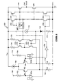
- FIG. 1 a prior art schematic diagram of an operational amplifier input stage having diode phase reversal protection is illustrated.
- a typical single power supply (ground and a positive voltage) input stage of a bipolar transistor integrated circuit operational amplifier (op amp) is generally indicated by the numeral 100.
- op amp bipolar transistor integrated circuit operational amplifier
- the op amp input stage 100 includes cross-coupled phase compensation diodes for preventing phase reversal, and current compensation diodes for preventing overshoot of the differential currents.
- a pair of differentially connected transistors 102 and 104 which can be either bipolar or junction field effect transistors (JFETs), have their current circuits connected together on one side to divide the output of a current source 106.
- a transistor's "current circuit” refers to the collector-emitter circuit of a bipolar transistor, or the source-drain circuit of a JFET; a transistor's "control circuit” refers to the base of a bipolar device, or the gate of an JFET.
- the differential transistors are bipolar pnp transistors.
- Input terminals 108 and 110 are adapted to receive differential input signals through series resistors 112 and 114.
- the transistors 102 and 104 divide the current from the current source 106 in mutual opposition, with the amount of current through each of the transistors 102 and 104 varying according to the relative input voltage signals applied to their bases from the input terminals 108 and 110, respectively. If a constant, known bias is applied to one of the input transistor bases, the magnitude of the signal at the base of the other input transistor can be determined by the amount of current flowing through that transistor.
- the input current source 106 operates from a positive voltage supply, V CC , while the collectors of the pnp input transistors 102 and 104 are connected to a negative voltage supply V- (preferably ground potential) through respective series-connected first and second trimmable input resistors 116 and 118.
- V- preferably ground potential
- the trimmable resistors 116 and 118 may be used to minimize any offset voltage of the input circuit.
- the input stage includes a folded cascode pair of active load npn bipolar transistors 120 and 122, whose emitters are connected to the collectors of input transistors 104 and 102, respectively.
- the bases of transistors 120 and 122 are connected together for common biasing.
- a bias circuit for the transistors 120 and 122 consists of a current source 124 that is connected to the bases of the transistors 120 and 122 and to a diode 126, which is connected through resistor 128 to ground potential.
- Diode 128 can be a diode-connected transistor.
- the magnitudes and relative phase of the currents flowing through the current circuits of transistors 120 and 122 are controlled by the base-emitter voltages, which are determined by the bias voltages at their bases and by the voltages across resistors 116 and 118.
- the base-emitter voltages control the bias current for the transistors 120 and 122.
- the active load is formed by a pair of pnp transistors 130 and 132, whose emitters are connected to V CC through resistors 134 and 136, respectively, and whose bases are connected together for common biasing.
- the transistor 130 base and collector are connected to the transistor 120 collector, and the transistor 132 collector is connected to the transistor 122 collector.
- the output current to the second stage (not illustrated) of the op amp is taken at the collector of transistor 132.
- the transistors 130 and 132 are connected as a current mirror, with the current through transistor 132 mirroring that through transistor 130. Any imbalance in the input signals at inputs 108 and 110 causes an imbalance in the currents through the transistors 120 and 122.
- the output current to the second stage reconciles the equal currents through transistors 130 and 132 with any current imbalance between transistors 120 and 122.
- the respectively connected transistor 102 or 104 collector current increases, which causes the respective resistor voltage to increase.
- the collector-base pn junction of its respective input transistor 102 or 104 becomes forward biased.
- the junction will forward bias for an input of approximately -400 mV at room temperature.
- the resistor voltages increase, it is possible that phase reversal can occur for input signals inside the CMR.
- a pair of phase compensation diodes 142 and 144 are cross-coupled between the bases and collectors of the transistors 102 and 104 to prevent phase reversal of the currents flowing through the transistors 120 and 122.
- the cross-coupled diode 142 or 144 connected to that input 108 or 110 conducts and reduces the voltage across the other resistor 118 or 116 to a smaller value to prevent phase reversal of the resistor voltages, and thus phase reversal of the currents in transistors 120 and 122.
- phase compensation diodes 142 and 144 conduct more current than the parasitic diodes 138 and 140 of the differential transistors 102 and 104, thus preventing phase reversal. In normal operation, the phase compensation diodes 142 and 144 are reverse biased and have no effect on the input circuit.
- the circuit illustrated in Figure 1 and described above is a conventional bipolar differential input op amp. While the operational amplifier 100 avoids phase reversal problems, the effect of forward biasing one of the parasitic diodes 138 or 140, and activating one of the cross-coupled diodes 142 or 144 is to reduce the voltages across the resistors 116 and 118 in response to the differential transistor's forward biased collector-base junction and the cross-coupled diode. Thus, the base-emitter voltages across the cascode transistors 120 and 122, and hence their bias currents increase so that their currents increase exponentially, on the order of twenty to thirty times their normal levels. These much higher current levels can cause the active load to malfunction and latch up the op amp.
- CMOS complementary metal oxide semiconductor
- the invention overcomes the above-identified problems as well as other shortcomings and deficiencies of existing technologies by providing, in an integrated circuit bipolar or JFET op amp, protection from output phase reversal from a forward biased collector-base parasitic pn diode of the input amplifier transistor and without having to rely upon input clamping diodes.
- at least two comparators are used to compare the op amp differential input voltages to a voltage reference (ground and/or power supply voltage(s)).
- P-channel metal oxide semiconductor (PMOS) transistors may be used for the differential pair of the comparator because a PMOS differential pair configuration includes ground in its common mode voltage range.
- comparators have an intentional mismatch so that the comparator switch point may be adjusted below ground, but above the point where the op amp input diode junctions become forward biased.
- this mismatch may be constructed by making the input transistor width to length (W/L) ratios different from each other. As the input is lowered below the switch point of the comparator, its output toggles to clamp the signal paths within the op amp so as to maintain the correct output phase state of the op amp.
- N-channel metal oxide semiconductor (NMOS) transistors may be used to include supply voltage, VDD, in its common mode voltage range.
- the comparators of the present invention use NMOS transistors for the differential pair so that V DD is included in the common-mode range of the comparator.
- both PMOS and NMOS transistors are used for the differential pairs in comparators that simultaneously compare the differential input signals to both Vss (low supply or ground) and V DD . If the input voltage should rise above V DD or below ground, the respective comparator toggles to clamp the internal op amp signal paths to maintain the correct output phase state of the op amp.
- a feature of the present invention is that a pair of comparators are used to monitor signal voltages on the differential inputs of a bipolar or JFET input op amp and prevent output phase reversal if these input signals go outside of a desired range.
- Another feature of the present invention is monitoring the op amp differential inputs for signals below the negative voltage or common ground reference of the power supply to the op amp by using a pair of PMOS comparators.
- Still another feature of the present invention is monitoring the op amp differential inputs for signals above the positive voltage reference of the power supply to the op amp by using a pair of NMOS comparators.
- Yet another feature of the present invention is monitoring the op amp differential inputs for signals below the negative voltage or common ground reference and above the positive voltage reference of the power supply to the op amp by using a pair of PMOS comparators and a pair of NMOS comparators, respectively.
- Still another feature is setting the clamping voltage setpoint by adjusting the mismatch (offset) of the comparator by making the input transistor W/L ratios different from each other.
- phase reversal protection comparators may be fabricated with a standard CMOS process.
- Another advantage of the present invention is that its phase reversal clamp voltage is more precise than that of a simple diode circuit.
- Still another advantage is that the clamping voltage is less sensitive to temperature and process variations, thus operation of the op amp is more robust.
- Yet another advantage is that the input comparators of the present invention are smaller than phase reversal diodes and thus require less area on the integrated circuit die.
- the invention protects an integrated circuit operational amplifier (op amp) from input voltage levels which may cause output phase reversal of the op amp.
- Embodiments of the invention comprise an integrated circuit op amp and voltage comparators which monitor the input voltages to the op amp differential input transistor pair.
- the op amp and comparators may be fabricated on an integrated circuit substrate and packaged in an integrated circuit package When the input voltage is of such a value which may cause output phase reversal, the outputs of the comparators are adapted to prevent the op amp output voltage from going into phase reversal.
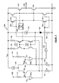
- FIG. 2 a schematic diagram of an operational amplifier according to an embodiment of the invention is illustrated.
- This operational amplifier is generally referenced by the numeral 200.
- Input terminals 108 and 110 are adapted to receive differential input signals through series resistors 112 and 114.
- the transistors 102 and 104 divide the current from the current source 106 in mutual opposition, with the amount of current through each of the transistors 102 and 104 varying according to the relative input voltage signals applied to their bases from the input terminals 108 and 110, respectively. If a constant, known bias is applied to one of the input transistor bases, the magnitude of the signal at the base of the other input transistor can be determined by the amount of current flowing through that transistor.
- the input current source 106 operates from a positive voltage supply, V DD , while the collectors of the pnp input transistors 102 and 104 are connected to a negative voltage supply V- (preferably ground potential) through respective series-connected first and second trimmable input resistors 116 and 118.
- V- preferably ground potential
- the trimmable resistors 116 and 118 may be used to minimize any offset voltage of the input circuit.
- the input stage includes a folded cascode pair of active load N-type metal oxide semiconductor (NMOS) transistors 220 and 222, whose sources are connected to the collectors of input transistors 104 and 102, respectively.
- the gates of transistors 220 and 222 are connected together for common biasing.
- a bias circuit for the transistors 220 and 222 consists of a current source 124 that is connected to the gates of the transistors 220 and 222 and to a diode 126, which is connected through resistor 128 to ground potential.
- Diode 128 can be a diode-connected transistor.
- the magnitudes and relative phase of the currents flowing through the current circuits of transistors 220 and 222 are controlled by the gate-source voltages, which are determined by the bias voltages at their gates and by the voltages across resistors 116 and 118.
- the gate-source voltages control the bias current for the transistors 220 and 222.
- the active load is formed by a pair of P-type metal oxide semiconductor (PMOS) transistors 230 and 232, whose sources are connected to V DD through resistors 134 and 136, respectively, and whose gates are connected together for common biasing.
- the transistor 230 gate and drain are connected to the transistor 220 drain, and the transistor 232 drain is connected to the transistor 222 drain.
- the output current to the output stage of the op amp is taken at the drains of transistors 222 and 232.
- a class AB control 240 is adapted to convert the single ended output from the transistors 222 and 232 to a differential output suitable for driving the output transistors 246 and 250.
- the transistors 230 and 232 are connected as a current mirror, with the current through transistor 232 mirroring that through transistor 230. Any imbalance in the input signals at the inputs 108 and 110 causes an imbalance in the currents through the transistors 220 and 222.
- the output current to the output stage reconciles the equal currents through transistors 230 and 232 with any current imbalance between transistors 220 and 222. As the input signal at the input 108 or 110 is decreased relative to the other input signal, the respectively connected transistor 102 or 104 collector current increases, which causes the respective resistor voltage to increase.
- comparators 500a and 500b monitor the negative voltage values at the bases of the transistors 102 and 104, respectively. Normally, these voltages are above (a greater positive value than) the threshold switch points of the comparators 500a and 500b so that the outputs of the comparators 500a and 500b are each at a logic "1" state.
- the output of the comparator 500a is at a logic 1 and PMOS transistors 242 and 244 are off, thereby not affecting the operation of the output transistor 246.
- the output of the comparator 500b is at a logic 1 the inverter 256 output is at a logic 0 and NMOS transistors 242 and 244 are off, thereby not affecting the operation of the output transistor 246.
- the inverter 256 output goes to a logic 1 and turns on transistors 252 and 254.
- transistor 254 no voltage is applied to the gate of output transistor 250 which effectively turns off transistor 250 (output 248 is determined by the output state of transistor 246).
- transistor 252 is on, a negative voltage (with respect to V DD ) is applied to the gate of output transistor 246 which effectively turns on transistor 246 (output 248 is connected to V DD ).
- the correct output phase of the op amp 200 is always maintained even when the collector-base pn junction of either transistor 102 or 104 becomes forward biased.
- FIG. 3 a schematic diagram of an operational amplifier according to another embodiment of the invention is illustrated.
- This operational amplifier is generally referenced by the numeral 300.
- General operation of the op amp 300 is the same as described hereinabove for the op amp 200 illustrated in Figure 2.
- comparators 600a and 600b monitor the positive voltage values at the bases of the transistors 102 and 104, respectively. Normally, these voltages are below (a more negative value than) the threshold switch points of the comparators 600a and 600b so that the outputs of the comparators 600a and 600b are each at a logic "1" state.
- the comparator 600b If the voltage at the input to the comparator 600b (base of transistor 104, negative differential input) goes above (more positive than V DD ) the comparator 600b threshold value then the output of the comparator 600b goes to a logic 0 and turns on transistors 242 and 244.
- transistor 242 When transistor 242 is on, a positive voltage is applied to the gate of output transistor 250 which effectively turns on transistor 250 (output 248 is connected to V- or ground).
- transistor 244 When transistor 244 is on, a positive voltage is applied to the gate of output transistor 246 which effectively turns off transistor 246 (output 248 is determined by the output state of transistor 250).
- the inverter 256 output goes to a logic 1 and turns on transistors 252 and 254.
- transistor 254 no voltage is applied to the gate of output transistor 250 which effectively turns off transistor 250 (output 248 is determined by the output state of transistor 246).
- transistor 252 is on, a negative voltage (with respect to V DD ) is applied to the gate of output transistor 246 which effectively turns on transistor 246 (output 248 is connected to V DD ).
- the correct output phase of the op amp 200 is always maintained.
- FIG. 4 a schematic diagram of an operational amplifier according to yet another embodiment of the invention is illustrated.
- This operational amplifier is generally referenced by the numeral 400.
- General operation of the op amp 400 is the same as described hereinabove for the op amp 200 illustrated in Figure 2.
- comparators 500a and 500b monitor the negative voltage values at the bases of the transistors 102 and 104, respectively. Normally, these voltages are above (a greater positive value than) the threshold switch points of the comparators 500a and 500b so that the outputs of the comparators 500a and 500b are each at a logic "1" state.
- the output of the comparator 500a is at a logic 1 and PMOS transistors 242 and 244 are off, thereby not affecting the operation of the output transistor 246.
- the output of the comparator 500b is at a logic 1 the inverter 256 output is at a logic 0 and NMOS transistors 242 and 244 are off, thereby not affecting the operation of the output transistor 246.
- Comparators 600a and 600b monitor the positive voltage values at the bases of the transistors 102 and 104, respectively. Normally, these voltages are below (a more negative value than) the threshold switch points of the comparators 600a and 600b so that the outputs of the comparators 600a and 600b are each at a logic "1" state. When the output of the comparator 600b is at a logic 1 and PMOS transistors 242 and 244 are off, thereby not affecting the operation of the output transistor 246. When the output of the comparator 600a is at a logic 1, the inverter 256 output is at a logic 0 and NMOS transistors 242 and 244 are off, thereby not affecting the operation of the output transistor 246.
- the inverter 256 output goes to a logic 1 and turns on transistors 252 and 254.
- transistor 254 no voltage is applied to the gate of output transistor 250 which effectively turns off transistor 250 (output 248 is determined by the output state of transistor 246).
- transistor 252 is on, a negative voltage (with respect to V DD ) is applied to the gate of output transistor 246 which effectively turns on transistor 246 (output 248 is connected to V DD ).
- the correct output phase of the op amp 400 is always maintained even when the collector-base pn junction of either transistor 102 or 104 becomes forward biased.
- the comparator 600b If the voltage at the input to the comparator 600b (base of transistor 104, negative differential input) goes above (more positive than V DD ) the comparator 600b threshold value then the output of the comparator 600b goes to a logic 0 and turns on transistors 242 and 244.
- transistor 242 When transistor 242 is on, a positive voltage is applied to the gate of output transistor 250 which effectively turns on transistor 250 (output 248 is connected to V- or ground).
- transistor 244 When transistor 244 is on, a positive voltage is applied to the gate of output transistor 246 which effectively turns off transistor 246 (output 248 is determined by the output state of transistor 250).
- the inverter 256 output goes to a logic 1 and turns on transistors 252 and 254.
- transistor 254 no voltage is applied to the gate of output transistor 250 which effectively turns off transistor 250 (output 248 is determined by the output state of transistor 246).
- transistor 252 is on, a negative voltage (with respect to V DD ) is applied to the gate of output transistor 246 which effectively turns on transistor 246 (output 248 is connected to V DD ).
- the correct output phase of the op amp 400 is always maintained.
- a circuit for a negative sense comparator is generally indicated by the numeral 500.
- PMOS transistors 502 and 504 are used for the differential input pair of the comparator 500 since this architecture includes ground in its common mode voltage range.
- the comparator 500 transistors 502 and 504 have an intentional mismatch so that the switch point of the comparator 500 is adjusted below ground or V- reference, but above the point where the collector-base junctions would become forward biased.
- this mismatch is constructed by making the input transistor (502 and 504) width to length W/L ratios different from each other. As the input is lowered below the switch point of the comparator 500, its output 506 toggles to ground (NMOS transistor 508 turns on).
- a circuit for a positive sense comparator is generally indicated by the numeral 600.
- NMOS transistors 602 and 604 are used for the differential input pair of the comparator 600 since this architecture includes V DD in its common mode voltage range.
- the comparator 600 transistors 602 and 604 have an intentional mismatch so that the switch point of the comparator 600 is adjusted above V DD , but below the point where the collector-base junctions would become forward biased.
- this mismatch is constructed by making the input transistor (602 and 604) width to length W/L ratios different from each other.
- the output 606 toggles to V DD (PMOS transistor 608 turns on).
Landscapes
- Engineering & Computer Science (AREA)
- Power Engineering (AREA)
- Amplifiers (AREA)
Abstract
Description
Claims (26)
- An integrated circuit operational amplifier having output phase reversal protection, comprising:an operational amplifier having differential inputs, wherein one of the differential inputs is a positive input and the other differential input is a negative input;a first comparator having a positive sense input connected to the positive input of the operational amplifier and sensing voltages thereon, a negative sense input connected to a first voltage and an output having first and second logic levels, wherein the output is at the first logic level when the positive sense input is at a voltage greater than or equal to the first voltage and the output is at the second logic level when the positive sense input is at a voltage less than the first voltage;a second comparator having a positive sense input connected to the negative input of the operational amplifier and sensing voltages thereon, a negative sense input connected to the first voltage and an output having first and second logic levels, wherein the output is at the first logic level when the positive sense input is at a voltage greater than or equal to the first voltage and the output is at the second logic level when the positive sense input is at a voltage less than the first voltage;the first comparator output is connected to first logic circuits of the operational amplifier such that when the first comparator output is at the second logic level the output of the operational amplifier is forced to a minimum voltage level; andthe second comparator output is connected to second logic circuits of the operational amplifier such that when the second comparator output is at the second logic level the output of the operational amplifier is forced to a maximum voltage level.
- The integrated circuit operational amplifier of claim 1, further comprising:a third comparator having a negative sense input connected to the positive input of the operational amplifier and sensing voltages thereon, a positive sense input connected to a second voltage and an output having first and second logic levels, wherein the output is at the first logic level when the negative sense input is at a voltage less than or equal to the second voltage and the output is at the second logic level when the negative sense input is at a voltage greater than the second voltage;a fourth comparator having a negative sense input connected to the negative input of the operational amplifier and sensing voltages thereon, a positive sense input connected to the second voltage and an output having first and second logic levels, wherein the output is at the first logic level when the negative sense input is at a voltage less than or equal to the second voltage and the output is at the second logic level when the negative sense input is at a voltage greater than the second voltage;the fourth comparator output is connected to the first logic circuits of the operational amplifier such that when the fourth comparator output is at the second logic level the output of the operational amplifier is forced to the minimum voltage level; andthe third comparator output is connected to the second logic circuits of the operational amplifier such that when the third comparator output is at the second logic level the output of the operational amplifier is forced to the maximum voltage level.
- An integrated circuit operational amplifier having output phase reversal protection, comprising:an operational amplifier having differential inputs, wherein one of the differential inputs is a positive input and the other differential input is a negative input;a third comparator having a negative sense input connected to the positive input of the operational amplifier and sensing voltages thereon, a positive sense input connected to a second voltage and an output having first and second logic levels, wherein the output is at the first logic level when the negative sense input is at a voltage less than or equal to the second voltage and the output is at the second logic level when the negative sense input is at a voltage greater than the second voltage;a fourth comparator having a negative sense input connected to the negative input of the operational amplifier and sensing voltages thereon, a positive sense input connected to the second voltage and an output having first and second logic levels, wherein the output is at the first logic level when the negative sense input is at a voltage less than or equal to the second voltage and the output is at the second logic level when the negative sense input is at a voltage greater than the second voltage;the fourth comparator output is connected to first logic circuits of the operational amplifier such that when the fourth comparator output is at the second logic level the output of the operational amplifier is forced to a minimum voltage level; andthe third comparator output is connected to second logic circuits of the operational amplifier such that when the third comparator output is at the second logic level the output of the operational amplifier is forced to a maximum voltage level.
- The integrated circuit operational amplifier of claim 1, wherein the operational amplifier is comprised of bipolar input transistors.
- The integrated circuit operational amplifier of claim 1, wherein the operational amplifier is comprised of junction field effect input transistors.
- The integrated circuit operational amplifier of claim 1, wherein the first and second comparators are comprised of N-channel and P-channel metal oxide semiconductor field effect transistors.
- The integrated circuit operational amplifier of claim 2, wherein the third and fourth comparators are comprised of N-channel and P-channel metal oxide semiconductor field effect transistors.
- The integrated circuit operational amplifier of claim 1, wherein the first logic circuits force output transistors of the operational amplifier to the minimum voltage level.
- The integrated circuit operational amplifier of claim 1, wherein the second logic circuits force output transistors of the operational amplifier to the maximum voltage level.
- The integrated circuit operational amplifier of claim 1, wherein the minimum voltage level is at about ground.
- The integrated circuit operational amplifier of claim 1, wherein the maximum voltage level is at about a supply voltage to the operational amplifier.
- The integrated circuit operational amplifier of claim 1, wherein the first logic level is a logic 1 and the second logic level is a logic 0.
- The integrated circuit operational amplifier of claim 1, wherein the first logic level is a logic 0 and the second logic level is a logic 1.
- The integrated circuit operational amplifier of claim 1, wherein the first voltage is at about ground.
- The integrated circuit operational amplifier of claim 1, wherein the second voltage is at about a supply voltage to the operational amplifier.
- The integrated circuit operational amplifier of claim 1, wherein the operational amplifier, and the first and second comparators are fabricated on a single integrated circuit die.
- The integrated circuit operational amplifier of claim 2, wherein the operational amplifier, and the first, second, third and fourth comparators are fabricated on a single integrated circuit die.
- The integrated circuit operational amplifier of claim 1, wherein the first comparator input transistors each have a different width to length ratio.
- The integrated circuit operational amplifier of claim 1, wherein the second comparator input transistors each have a different width to length ratio.
- The integrated circuit operational amplifier of claim 1, wherein the third comparator input transistors each have a different width to length ratio.
- The integrated circuit operational amplifier of claim 1, wherein the fourth comparator input transistors each have a different width to length ratio.
- A method for protecting an integrated circuit operational amplifier from output phase reversal, the operational amplifier having positive and negative differential inputs, said method comprising the steps of:comparing a voltage on the positive input of the operational amplifier to a first voltage with a first comparator, wherein the first comparator output is at a first logic level when the voltage on the positive input of the operational amplifier is greater than or equal to the first voltage and the first comparator output is at a second logic level when the voltage on the positive input of the operational amplifier is less than the first voltage;comparing another voltage on the negative input of the operational amplifier to the first voltage with a second comparator, wherein the second comparator output is at a first logic level when the another voltage on the negative input of the operational amplifier is greater than or equal to the first voltage and the second comparator output is at a second logic level when the another voltage on the negative input of the operational amplifier is less than the first voltage;forcing the operational amplifier output to a minimum voltage level when the first comparator output is at the second logic level; andforcing the operational amplifier output to a maximum voltage level when the second comparator output is at the second logic level.
- The method of claim 22, further comprising the steps of:comparing the voltage on the positive input of the operational amplifier to a second voltage with a third comparator, wherein the third comparator output is at a first logic level when the voltage on the positive input of the operational amplifier is less than or equal to the second voltage and the third comparator output is at a second logic level when the voltage on the positive input of the operational amplifier is greater than the second voltage;comparing the another voltage on the negative input of the operational amplifier to the second voltage with a fourth comparator, wherein the second comparator output is at a first logic level when the another voltage on the negative input of the operational amplifier is less than or equal to the second voltage and the second comparator output is at a second logic level when the another voltage on the negative input of the operational amplifier is greater than the second voltage;forcing the operational amplifier output to a minimum voltage level when the fourth comparator output is at the second logic level; andforcing the operational amplifier output to a maximum voltage level when the third comparator output is at the second logic level.
- A method for protecting an integrated circuit operational amplifier from output phase reversal, the operational amplifier having positive and negative differential inputs, said method comprising the steps of:comparing a voltage on the positive input of the operational amplifier to a second voltage with a third comparator, wherein the third comparator output is at a first logic level when the voltage on the positive input of the operational amplifier is less than or equal to the second voltage and the third comparator output is at a second logic level when the voltage on the positive input of the operational amplifier is greater than the second voltage;comparing another voltage on the negative input of the operational amplifier to the second voltage with a fourth comparator, wherein the second comparator output is at a first logic level when the another voltage on the negative input of the operational amplifier is less than or equal to the second voltage and the second comparator output is at a second logic level when the another voltage on the negative input of the operational amplifier is greater than the second voltage;forcing the operational amplifier output to a minimum voltage level when the fourth comparator output is at the second logic level; andforcing the operational amplifier output to a maximum voltage level when the third comparator output is at the second logic level.
- The method of claim 23, wherein the minimum voltage level is at about ground and the maximum voltage level is at about a supply voltage to the operational amplifier.
- The method of claim 24, wherein the minimum voltage level is at about ground and the maximum voltage level is at about a supply voltage to the operational amplifier.
Applications Claiming Priority (2)
| Application Number | Priority Date | Filing Date | Title |
|---|---|---|---|
| US537626 | 2000-03-29 | ||
| US09/537,626 US6218900B1 (en) | 2000-03-29 | 2000-03-29 | Operational amplifier phase reversal protection |
Publications (2)
| Publication Number | Publication Date |
|---|---|
| EP1143610A2 true EP1143610A2 (en) | 2001-10-10 |
| EP1143610A3 EP1143610A3 (en) | 2004-09-22 |
Family
ID=24143444
Family Applications (1)
| Application Number | Title | Priority Date | Filing Date |
|---|---|---|---|
| EP01106642A Withdrawn EP1143610A3 (en) | 2000-03-29 | 2001-03-16 | Operational amplifier phase reversal protection |
Country Status (6)
| Country | Link |
|---|---|
| US (2) | US6218900B1 (en) |
| EP (1) | EP1143610A3 (en) |
| JP (1) | JP2001308656A (en) |
| KR (1) | KR20010093718A (en) |
| CN (1) | CN1318899A (en) |
| TW (1) | TW492238B (en) |
Families Citing this family (30)
| Publication number | Priority date | Publication date | Assignee | Title |
|---|---|---|---|---|
| US6404266B1 (en) * | 2000-07-25 | 2002-06-11 | National Semiconductor Corporation | Differential input stage with bias current reduction for latch-up prevention |
| DE10038321A1 (en) * | 2000-08-05 | 2002-02-14 | Philips Corp Intellectual Pty | Adaptation circuit for audio and video signals |
| JP2002151966A (en) * | 2000-11-14 | 2002-05-24 | Pioneer Electronic Corp | Isolator circuit |
| US6703900B2 (en) * | 2002-06-05 | 2004-03-09 | Texas Instruments Incorporated | Fast, stable overload recovery circuit and method |
| US6933784B2 (en) * | 2003-11-05 | 2005-08-23 | Texas Instruments Incorporated | Output stage for high gain and low distortion operational amplifier |
| JP3874776B2 (en) * | 2004-10-15 | 2007-01-31 | ローム株式会社 | Operational amplifier |
| JP2008197723A (en) * | 2007-02-08 | 2008-08-28 | Toshiba Corp | Voltage generation circuit |
| DE602007007433D1 (en) * | 2007-04-06 | 2010-08-12 | St Microelectronics Des & Appl | Amplifier with output protection, in particular operational amplifier for audio application |
| JP4657252B2 (en) * | 2007-06-04 | 2011-03-23 | 三洋電機株式会社 | Charge pump circuit and slice level control circuit |
| US7777526B2 (en) * | 2008-06-06 | 2010-08-17 | Altera Corporation | Increased sensitivity and reduced offset variation in high data rate HSSI receiver |
| JP5022318B2 (en) * | 2008-07-16 | 2012-09-12 | 新日本無線株式会社 | Operational amplifier |
| KR101699956B1 (en) * | 2009-08-12 | 2017-01-25 | 톰슨 라이센싱 | Method and system for crosstalk and distortion corrections for three-dimensional (3d) projection |
| CN101860368B (en) * | 2010-05-10 | 2012-12-05 | 中国电子科技集团公司第五十八研究所 | Negative-voltage effective transmission circuit suitable for standard CMOS process |
| TWI456221B (en) * | 2011-01-21 | 2014-10-11 | Chroma Ate Inc | Electronic load with analog light-emitting diode characteristics |
| JP5795934B2 (en) * | 2011-10-17 | 2015-10-14 | 新日本無線株式会社 | Operational amplifier |
| US8823457B1 (en) * | 2012-12-17 | 2014-09-02 | Google Inc. | Short circuit current protection in an amplifier |
| CN104360130A (en) * | 2014-11-05 | 2015-02-18 | 中国电子科技集团公司第四十三研究所 | Method for testing input current of magnetic isolation amplifier |
| CN104661170A (en) * | 2015-03-09 | 2015-05-27 | 山东省计算中心(国家超级计算济南中心) | Fault detection system for multiple speakers |
| US10296026B2 (en) * | 2015-10-21 | 2019-05-21 | Silicon Laboratories Inc. | Low noise reference voltage generator and load regulator |
| CN207283503U (en) * | 2017-07-27 | 2018-04-27 | 广州联星科技有限公司 | Bidirectional current adapter power amplifier biasing circuit |
| US10917058B2 (en) * | 2018-07-06 | 2021-02-09 | Texas Instruments Incorporated | Servo-amplifier with closed-loop biasing |
| TWI716817B (en) * | 2019-02-19 | 2021-01-21 | 立積電子股份有限公司 | Power detector with all transistors being bipolar junction transistors |
| JP7431528B2 (en) * | 2019-08-08 | 2024-02-15 | 株式会社東芝 | semiconductor amplifier circuit |
| CN113037236B (en) * | 2019-12-09 | 2022-10-14 | 圣邦微电子(北京)股份有限公司 | Operational amplifier |
| JP7388914B2 (en) * | 2019-12-24 | 2023-11-29 | 日清紡マイクロデバイス株式会社 | operational amplifier |
| CN111371458A (en) * | 2020-03-16 | 2020-07-03 | 长江存储科技有限责任公司 | A voltage amplifier circuit and multiplying digital-to-analog converter |
| CN114584088B (en) * | 2020-12-02 | 2024-10-18 | 圣邦微电子(北京)股份有限公司 | Operational amplifier, integrated circuit, and internal power generation method of operational amplifier |
| CN114614456B (en) * | 2020-12-04 | 2025-06-10 | 南京宏泰半导体科技股份有限公司 | Clamping system and method |
| US12489405B2 (en) * | 2021-09-22 | 2025-12-02 | Texas Instruments Incorporated | Amplifier output stage circuitry |
| CN115664359B (en) * | 2022-09-08 | 2025-10-24 | 北京微科能创科技有限公司 | A topological circuit combining an operational amplifier and a comparator |
Family Cites Families (7)
| Publication number | Priority date | Publication date | Assignee | Title |
|---|---|---|---|---|
| US3990020A (en) * | 1975-06-26 | 1976-11-02 | Hughes Aircraft Company | DC linear power amplifier |
| NL7902160A (en) * | 1979-03-20 | 1980-09-23 | Philips Nv | POWER AMPLIFIER WITH NON-LINEAR COUPLING. |
| US4823227A (en) * | 1985-09-16 | 1989-04-18 | Sta-Con, Inc. | Three-phase monitor circuitry |
| US4871980A (en) * | 1987-03-18 | 1989-10-03 | Zdzislaw Gulczynski | High efficiency power amplifier comprising multilevel power supply |
| US4866398A (en) * | 1988-04-12 | 1989-09-12 | Zdzislaw Gulczynski | Analog power amplifier |
| US5153529A (en) * | 1991-08-30 | 1992-10-06 | Motorola, Inc. | Rail-to-rail input stage of an operational amplifier |
| US5418491A (en) | 1994-07-07 | 1995-05-23 | Analog Devices, Inc. | Operational amplifier compensation circuit for preventing phase reversal and maintaining performance for inputs outside the common mode range |
-
2000
- 2000-03-29 US US09/537,626 patent/US6218900B1/en not_active Expired - Lifetime
-
2001
- 2001-03-16 EP EP01106642A patent/EP1143610A3/en not_active Withdrawn
- 2001-03-27 KR KR1020010015978A patent/KR20010093718A/en not_active Withdrawn
- 2001-03-28 JP JP2001094420A patent/JP2001308656A/en not_active Withdrawn
- 2001-03-29 CN CN01112142A patent/CN1318899A/en active Pending
- 2001-03-29 TW TW090107507A patent/TW492238B/en not_active IP Right Cessation
- 2001-04-16 US US09/836,612 patent/US6509797B2/en not_active Expired - Lifetime
Also Published As
| Publication number | Publication date |
|---|---|
| EP1143610A3 (en) | 2004-09-22 |
| JP2001308656A (en) | 2001-11-02 |
| CN1318899A (en) | 2001-10-24 |
| US6509797B2 (en) | 2003-01-21 |
| US20010026193A1 (en) | 2001-10-04 |
| US6218900B1 (en) | 2001-04-17 |
| TW492238B (en) | 2002-06-21 |
| KR20010093718A (en) | 2001-10-29 |
Similar Documents
| Publication | Publication Date | Title |
|---|---|---|
| US6218900B1 (en) | Operational amplifier phase reversal protection | |
| US5095284A (en) | Subthreshold CMOS amplifier with wide input voltage range | |
| US8633770B2 (en) | Current sense amplifier having bipolar common mode input range | |
| EP2033314B1 (en) | Differential amplifier with over-voltage protection and method | |
| US4766394A (en) | Operational amplifier circuit having wide operating range | |
| US5739712A (en) | Power amplifying circuit having an over-current protective function | |
| JPH0667744A (en) | Constant-voltage circuit | |
| WO1997009778A1 (en) | gm-CONTROL FOR CMOS RAIL-TO-RAIL INPUT STAGES BY REGULATING THE SUM OF THE GATE-SOURCE VOLTAGES CONSTANT | |
| US7385433B2 (en) | Analog switch with reduced parasitic bipolar transistor injection | |
| KR20190113551A (en) | Voltage regulator | |
| US6326847B1 (en) | High gain, high speed, rail-to-rail amplifier | |
| JP3593486B2 (en) | Voltage comparison circuit and substrate bias adjustment circuit using the same | |
| US5418491A (en) | Operational amplifier compensation circuit for preventing phase reversal and maintaining performance for inputs outside the common mode range | |
| KR20190010471A (en) | Magnetic sensor circuit | |
| US7737784B2 (en) | Self configuring output stages of precision amplifiers | |
| US6822513B1 (en) | Symmetric and complementary differential amplifier | |
| US4240039A (en) | MOS Differential amplifier | |
| US7109794B2 (en) | Differential gain stage for low voltage supply | |
| US7394308B1 (en) | Circuit and method for implementing a low supply voltage current reference | |
| JP2000004129A (en) | CMOS analog circuit | |
| US20240348220A1 (en) | Amplifier circuit with dynamic output slope compensation for driving large capacitive loads | |
| US20240056044A1 (en) | Precision operational amplifier using floating input stage | |
| US11876496B2 (en) | Differential input circuits with input voltage protection | |
| US10826443B2 (en) | Common mode overload recovery for amplifier | |
| JP2025115267A (en) | Operational amplifier |
Legal Events
| Date | Code | Title | Description |
|---|---|---|---|
| PUAI | Public reference made under article 153(3) epc to a published international application that has entered the european phase |
Free format text: ORIGINAL CODE: 0009012 |
|
| 17P | Request for examination filed |
Effective date: 20010316 |
|
| AK | Designated contracting states |
Kind code of ref document: A2 Designated state(s): AT BE CH CY DE DK ES FI FR GB GR IE IT LI LU MC NL PT SE TR |
|
| AX | Request for extension of the european patent |
Free format text: AL;LT;LV;MK;RO;SI |
|
| PUAL | Search report despatched |
Free format text: ORIGINAL CODE: 0009013 |
|
| AK | Designated contracting states |
Kind code of ref document: A3 Designated state(s): AT BE CH CY DE DK ES FI FR GB GR IE IT LI LU MC NL PT SE TR |
|
| AX | Request for extension of the european patent |
Extension state: AL LT LV MK RO SI |
|
| AKX | Designation fees paid |
Designated state(s): AT BE CH CY DE DK ES FI FR GB GR IE IT LI LU MC NL PT SE TR |
|
| STAA | Information on the status of an ep patent application or granted ep patent |
Free format text: STATUS: THE APPLICATION IS DEEMED TO BE WITHDRAWN |
|
| 18D | Application deemed to be withdrawn |
Effective date: 20050323 |