EP1143519A2 - Apparatus and method for assembling optical devices - Google Patents
Apparatus and method for assembling optical devices Download PDFInfo
- Publication number
- EP1143519A2 EP1143519A2 EP01302771A EP01302771A EP1143519A2 EP 1143519 A2 EP1143519 A2 EP 1143519A2 EP 01302771 A EP01302771 A EP 01302771A EP 01302771 A EP01302771 A EP 01302771A EP 1143519 A2 EP1143519 A2 EP 1143519A2
- Authority
- EP
- European Patent Office
- Prior art keywords
- substrate
- mounting structure
- protrusions
- well
- material system
- Prior art date
- Legal status (The legal status is an assumption and is not a legal conclusion. Google has not performed a legal analysis and makes no representation as to the accuracy of the status listed.)
- Withdrawn
Links
Images



Classifications
-
- G—PHYSICS
- G02—OPTICS
- G02B—OPTICAL ELEMENTS, SYSTEMS OR APPARATUS
- G02B6/00—Light guides; Structural details of arrangements comprising light guides and other optical elements, e.g. couplings
- G02B6/24—Coupling light guides
- G02B6/42—Coupling light guides with opto-electronic elements
- G02B6/4201—Packages, e.g. shape, construction, internal or external details
- G02B6/4219—Mechanical fixtures for holding or positioning the elements relative to each other in the couplings; Alignment methods for the elements, e.g. measuring or observing methods especially used therefor
- G02B6/4236—Fixing or mounting methods of the aligned elements
- G02B6/4239—Adhesive bonding; Encapsulation with polymer material
-
- H—ELECTRICITY
- H10—SEMICONDUCTOR DEVICES; ELECTRIC SOLID-STATE DEVICES NOT OTHERWISE PROVIDED FOR
- H10W—GENERIC PACKAGES, INTERCONNECTIONS, CONNECTORS OR OTHER CONSTRUCTIONAL DETAILS OF DEVICES COVERED BY CLASS H10
- H10W70/00—Package substrates; Interposers; Redistribution layers [RDL]
- H10W70/60—Insulating or insulated package substrates; Interposers; Redistribution layers
- H10W70/67—Insulating or insulated package substrates; Interposers; Redistribution layers characterised by their insulating layers or insulating parts
- H10W70/68—Shapes or dispositions thereof
-
- H—ELECTRICITY
- H10—SEMICONDUCTOR DEVICES; ELECTRIC SOLID-STATE DEVICES NOT OTHERWISE PROVIDED FOR
- H10W—GENERIC PACKAGES, INTERCONNECTIONS, CONNECTORS OR OTHER CONSTRUCTIONAL DETAILS OF DEVICES COVERED BY CLASS H10
- H10W72/00—Interconnections or connectors in packages
- H10W72/071—Connecting or disconnecting
- H10W72/073—Connecting or disconnecting of die-attach connectors
-
- H—ELECTRICITY
- H10—SEMICONDUCTOR DEVICES; ELECTRIC SOLID-STATE DEVICES NOT OTHERWISE PROVIDED FOR
- H10W—GENERIC PACKAGES, INTERCONNECTIONS, CONNECTORS OR OTHER CONSTRUCTIONAL DETAILS OF DEVICES COVERED BY CLASS H10
- H10W72/00—Interconnections or connectors in packages
- H10W72/071—Connecting or disconnecting
- H10W72/073—Connecting or disconnecting of die-attach connectors
- H10W72/07321—Aligning
- H10W72/07327—Aligning involving guiding structures, e.g. spacers or supporting members
-
- H—ELECTRICITY
- H10—SEMICONDUCTOR DEVICES; ELECTRIC SOLID-STATE DEVICES NOT OTHERWISE PROVIDED FOR
- H10W—GENERIC PACKAGES, INTERCONNECTIONS, CONNECTORS OR OTHER CONSTRUCTIONAL DETAILS OF DEVICES COVERED BY CLASS H10
- H10W72/00—Interconnections or connectors in packages
- H10W72/071—Connecting or disconnecting
- H10W72/073—Connecting or disconnecting of die-attach connectors
- H10W72/07331—Connecting techniques
- H10W72/07337—Connecting techniques using a polymer adhesive, e.g. an adhesive based on silicone or epoxy
-
- H—ELECTRICITY
- H10—SEMICONDUCTOR DEVICES; ELECTRIC SOLID-STATE DEVICES NOT OTHERWISE PROVIDED FOR
- H10W—GENERIC PACKAGES, INTERCONNECTIONS, CONNECTORS OR OTHER CONSTRUCTIONAL DETAILS OF DEVICES COVERED BY CLASS H10
- H10W72/00—Interconnections or connectors in packages
- H10W72/071—Connecting or disconnecting
- H10W72/073—Connecting or disconnecting of die-attach connectors
- H10W72/07351—Connecting or disconnecting of die-attach connectors characterised by changes in properties of the die-attach connectors during connecting
- H10W72/07353—Connecting or disconnecting of die-attach connectors characterised by changes in properties of the die-attach connectors during connecting changes in shapes
-
- H—ELECTRICITY
- H10—SEMICONDUCTOR DEVICES; ELECTRIC SOLID-STATE DEVICES NOT OTHERWISE PROVIDED FOR
- H10W—GENERIC PACKAGES, INTERCONNECTIONS, CONNECTORS OR OTHER CONSTRUCTIONAL DETAILS OF DEVICES COVERED BY CLASS H10
- H10W72/00—Interconnections or connectors in packages
- H10W72/30—Die-attach connectors
- H10W72/331—Shapes of die-attach connectors
- H10W72/334—Cross-sectional shape, i.e. in side view
-
- H—ELECTRICITY
- H10—SEMICONDUCTOR DEVICES; ELECTRIC SOLID-STATE DEVICES NOT OTHERWISE PROVIDED FOR
- H10W—GENERIC PACKAGES, INTERCONNECTIONS, CONNECTORS OR OTHER CONSTRUCTIONAL DETAILS OF DEVICES COVERED BY CLASS H10
- H10W72/00—Interconnections or connectors in packages
- H10W72/30—Die-attach connectors
- H10W72/351—Materials of die-attach connectors
- H10W72/353—Materials of die-attach connectors not comprising solid metals or solid metalloids, e.g. ceramics
- H10W72/354—Materials of die-attach connectors not comprising solid metals or solid metalloids, e.g. ceramics comprising polymers
-
- H—ELECTRICITY
- H10—SEMICONDUCTOR DEVICES; ELECTRIC SOLID-STATE DEVICES NOT OTHERWISE PROVIDED FOR
- H10W—GENERIC PACKAGES, INTERCONNECTIONS, CONNECTORS OR OTHER CONSTRUCTIONAL DETAILS OF DEVICES COVERED BY CLASS H10
- H10W72/00—Interconnections or connectors in packages
- H10W72/90—Bond pads, in general
- H10W72/931—Shapes of bond pads
Definitions
- the invention generally relates to optical devices and their fabrication, and more particularly to an apparatus and method for precisely controlling the angular relationship between optical elements and a substrate plane within an optical device.
- Optical filters are well known for use with optical devices, such as, for example, hybrid optical components.
- Conventional assembly methodologies for constructing optical devices, such as hybrid optical components are generally designed such that optical elements are mounted in a single structural plane.
- optical elements such as mirrors, filters, polarizers, beam splitters, lenses and other reflective or transmissive optical elements within the optical device are positioned and bonded in a single plane on a substrate surface. It is important to properly align the optical filters and other optical elements along the structural plane so that optical signal is not lost through improper transmission from one optical element to another.
- optical elements utilized in optical devices have been epoxied or otherwise affixed to a substrate surface.
- an optical device 10 is shown having a carrier substrate 12.
- the optical device 10 has an optical input point 14 and an optical output point 40 positioned in the same structural plane.
- Further mounted on the carrier substrate 12 are a first optical element 18, a second optical element 28, and a third optical element 34, all mounted in the same structural plane.
- the optical elements 18, 28, 34 may be any reflective or transmissive optical elements, such as lenses, mirrors, polarizers, beam splitters, filters, or other like optical elements.
- the first optical element 18 has a first surface 20 (FIG. 2), a second surface 22, and a reflecting surface 24.
- optical signals from the input point 14 are to travel along a first signal pathway 16 and be reflected off of the reflecting surface 24 toward the second optical element 28.
- the reflected optical signals travel along a second signal pathway 26 and reflect off of a reflecting surface 30 of the second optical element 28.
- the twice reflected optical signals then travel along a third signal pathway 32 and are reflected off of a reflecting surface 36 of the third optical element 34 into a fourth signal pathway 38 leading to the output point 40.
- the optical elements 18, 28, 34 generally are affixed to the carrier substrate 12 through an epoxy 42.
- the epoxy 42 is deposited on a first surface 13 of the carrier substrate 12 and the optical elements 18, 28, 34 are each lowered into contact with the epoxy 42.
- the optical element does not bond with the carrier substrate 12 such that the first surface 20 is parallel to the first surface 13.
- the first optical element 18 has been lowered onto the epoxy 42, but remains at an angle to the first surface 13 of the carrier substrate 12. Improper alignment of the optical elements 18, 28, 34 leads to the transmission of optical signals out of the structural plane, thereby preventing the optical signals from reaching the output point 40.
- the invention provides a mounting structure for mounting an optical element.
- the mounting structure includes a substrate having a first surface, a plurality of protrusions extending by a substantially equal amount from the substrate first surface, and one or more walls extending from the substrate first surface and surrounding the protrusions and defining a well.
- the invention further provides an optical device which includes a substrate having a first surface, at least one mounting structure, and at least one optical element mounted on protrusions of the at least one mounting structure.
- the invention further provides a method of mounting one or more optical elements onto an optical device having one or more mounting structures which include a plurality of protrusions surrounded by one or more walls defining a space.
- the method includes the steps of adding an epoxy material to the space, lowering the optical element into contact with the epoxy material, contacting the optical element to the protrusions, and curing the epoxy material.
- the invention further provides a method of planarly aligning two or more optical elements mounted onto an optical device having two or more mounting structures which include a plurality of protrusions surrounded by one or more walls defining a space.
- the method includes the steps of adding an epoxy material to the space of each mounting structure, lowering each optical element into contact with the epoxy material in a respective space, contacting each optical element to the protrusions of a respective mounting structure, aligning each optical element to the other optical elements, and curing the epoxy material.
- FIG. 1 is a view from the top of a conventional optical device on a carrier substrate.
- FIG. 2 is a cross-sectional view taken along line II-II of FIG. 1.
- FIG. 3 is another cross-sectional view showing improper alignment of an optical element of the optical device of FIG. 1.
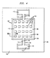
- FIG. 4 is a view from the top of an optical device carrier substrate constructed in accordance with an embodiment of the present invention.
- FIG. 5 is a cross-sectional view taken along line V-V of FIG. 4 of an optical element being mounted on the carrier substrate.
- FIG. 6 is another cross-sectional view of the optical element being mounted on the carrier substrate of FIG. 4.
- FIG. 7 is another cross-sectional view of the optical device being mounted on the carrier substrate of FIG. 4.
- FIG. 8 is a partial cross-sectional view taken along line VIII-VIII of FIG. 4.
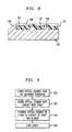
- FIG. 9 is a flow diagram of the process of aligning optical elements on a carrier substrate in accordance with an embodiment of the present invention.
- the optical device carrier substrate 100 has a first surface 102. Located on the first surface 102 is a mounting structure 103 including a generally rectangular well 108 with walls 106 defining a space 109. A plurality of island-like protrusions 104 are positioned within the space 109. Preferably, each of the protrusions 104 extends upwardly the same distance above the first surface 102. In a preferred embodiment, the walls 106 extend to a greater height above the first surface 102 than do the protrusions 104. A pair of reservoirs 112 are positioned at opposite ends of the well 108. Each reservoir 112 is connected to the well 108 through a conduit 114 having walls 116.
- a material system 110 which preferably has the characteristics that it efficiently wets a surface, is adhesive, and has weak cohesive forces, is placed within the well 108 filling in the space 109 to at least just above an uppermost extent of the protrusions 104 (FIGS. 6, 8).
- the efficient wetting surface allows for a thin layer of the adhesive material system 110 to be used to adhere optical elements to the protrusions 104.
- a preferred embodiment of the adhesive material system 110 is an epoxy, either in liquid or powder form. If in the powder form, the epoxy preferably would have to be subjected to conditions transitioning it into a liquid phase, such as, for example, a temperature or pressure change.
- Another example of the adhesive material system 110 is a wax-like material. As with the powdered epoxy, a wax-like material preferably would have to be subjected to conditions transitioning it into a liquid phase, such as, for example, a temperature or pressure change.
- the conduits 114 allow for the egress of the adhesive material system 110 from the space 109 into the reservoirs 112 during mounting of optical elements, such as the optical elements 18, 28, 34.
- the mounting structure 103 namely the protrusions 104, well 108, reservoirs 112, and conduits 114, are preferentially formed through standard anisotropic etching of a substrate, e.g. a semiconductor substrate.
- the carrier substrate 100 is only partially shown in FIG. 4.
- the plurality of protrusions 104 of FIG. 4 are designed to support a single optical element 18, 28, 34.
- structures 103 which are the same as or similar to those shown in FIG. 4 are also provided in the substrate 12 to support other respective ones of the optical elements 18, 28, 34.
- substrate is to be understood as including any material which is capable of supporting an optical element. Industry preferred materials include ceramic, glass, silicon, steel, metal alloys, and diamond.
- step 200 the adhesive material system 110 is added to the space 109 within the walls 106.
- An optical element e.g. 18, is then lowered over the mounting structure 103 into the space 109 as shown in FIG. 5.
- the adhesive material system 110 is omitted from FIG. 5 for clarity of illustration regarding the lowering of the optical element 18.
- the optical element 18 is further lowered until it comes in contact with the adhesive material system 110 at step 202 (FIGS. 6, 7, 9).
- step 204 the optical element 18 is positioned to contact at least two protrusions 104 (FIGS. 7, 9).
- the illustrated mounting structure 103 which includes more than two protrusions 104, is configured to receive a single optical element.
- the volume of the optical element 18 will displace an equal volume of the adhesive material system 110, forcing the adhesive material system 110 through the conduits 114 into the reservoirs 112.
- the adhesive material system 110 is cured. With a proper formulation of the material system 110 and a proper drying temperature, the adhesive material system 110 preferably will tend to decrease its volume through curing and cooling, thereby forcing the optical element 18 into a state of tension. This will ensure accurate alignment and improve the stability of the mounted optical element 18.
- the method thus described can be repeated as many times as necessary to mount all the required optical elements. Further, the curing step 204 can be postponed until after all the optical elements are properly mounted and aligned to ensure that the optical signal pathway leads to the output point 40 or similar output.
- the mounting structure 103 is applicable for any semiconductor structures which require planar alignment.
- the walls 106 are shown in a generally rectangular position, any suitable shape may be employed. Accordingly, the invention is not to be seen as limited by the foregoing description, but is only limited by the scope of the appended claims.
Landscapes
- Physics & Mathematics (AREA)
- General Physics & Mathematics (AREA)
- Optics & Photonics (AREA)
- Light Receiving Elements (AREA)
- Led Device Packages (AREA)
- Optical Couplings Of Light Guides (AREA)
- Mounting And Adjusting Of Optical Elements (AREA)
Abstract
Description
Claims (33)
- A mounting structure for mounting a semiconductor element, comprising:a substrate having a first surface;a plurality of protrusions extending from said substrate first surface; andone or more walls extending from said substrate first surface and surrounding said protrusions and defining a well.
- The mounting structure of claim 1, wherein the well is adapted to contain an adhesive material system.
- The mounting structure of claim 2, further comprising at least one reservoir provided in said substrate and connected with said well to receive said adhesive material system from said well.
- The mounting structure of claim 3, comprising two said reservoirs.
- The mounting structure of claim 4, further comprising a pair of conduits, each said conduit connecting a respective said reservoir with said well.
- The mounting structure of claim 1, wherein said protrusions are configured to receive an optical element.
- The mounting structure of claim 1, wherein said walls extend above said protrusions.
- The mounting structure of claim 1, wherein said plurality of protrusions extend by a substantially equal amount from said substrate first surface
- The mounting structure of claim 1, wherein the mounting structure is adapted for mounting an optical element.
- The mounting structure of claim 5, wherein said walls are formed from said substrate.
- The mounting structure of claim 10, wherein said walls are formed by an anisotropic etch of said substrate.
- The mounting structure of claim 11, wherein said protrusions are formed from said substrate.
- The mounting structure of claim 12, wherein said protrusions are formed by an anisotropic etch of said substrate.
- The mounting structure of claim 13, wherein said reservoirs are formed from said substrate.
- The mounting structure of claim 14, wherein said reservoirs are formed by an anisotropic etch of said substrate.
- The mounting structure of claim 15, wherein said conduits are formed from said substrate.
- The mounting structure of claim 16, wherein said conduits are formed by an anisotropic etch of said substrate.
- A carrier substrate for use with a plurality of semiconductor elements, comprising:a substrate having a first surface; anda plurality of mounting structures as claimed in any of claims 1 to 8 having said substrate in common.
- A semiconductor device, comprising:a substrate having a first surface;at least one mounting structure including:a plurality of protrusions extending from said substrate first surface; andone or more walls extending from said substrate first surfaceand surrounding said protrusions and defining a well; andat least one optical element mounted on and adhered to said protrusions.
- The semiconductor device of claim 19 comprising a plurality of optical elements, each said element mounted on said protrusions of a respective said mounting structure such that each said element is planarly aligned relative to each other said element.
- The optical device of claim 20 wherein said walls extend above said protrusions.
- The semiconductor device of claim 19 wherein said plurality of protrusions extend by a substantially equal amount from said substrate first surface
- The semiconductor device of claim 21 wherein each said well is adapted to contain an adhesive material system.
- The semiconductor device of claim 23 wherein said adhesive material system is an epoxy.
- The semiconductor device of claim 24 wherein each said optical element is mounted on and adhered to said protrusions by said epoxy.
- The semiconductor device of claim 24 further comprising at least one reservoir provided in said substrate connected with each said well.
- The semiconductor device of claim 26 comprising two said reservoirs for each said mounting structure.
- The semiconductor device of claim 27 further comprising a pair of conduits for each said mounting structure, each said conduit connecting a respective said reservoir with each said well.
- A method of mounting one or more semiconductor elements onto a semiconductor device having one or more mounting structures which include a plurality of protrusions surrounded by one or more walls defining a well, comprising the steps of:providing an adhesive material system in said well including at locations above said protrusions;lowering said semiconductor element into contact with said adhesive material system;contacting said semiconductor element to said protrusions; andcuring said adhesive material system.
- The method of claim 29 wherein said adhesive material system is added to a level which extends above said protrusions.
- The method of claim29 wherein said curing of the adhesive material system places the semiconductor element in tension.
- The method of claim 29 wherein said semiconductor element comprises an optical element.
- The method of any of claims 29 to 32, wherein there are two or more said semiconductor elements and including aligning each said semiconductor element to the other semiconductor elements prior to said curing step.
Applications Claiming Priority (2)
| Application Number | Priority Date | Filing Date | Title |
|---|---|---|---|
| US09/542,937 US6404566B1 (en) | 2000-04-04 | 2000-04-04 | Apparatus and method for assembling optical devices |
| US542937 | 2000-04-04 |
Publications (2)
| Publication Number | Publication Date |
|---|---|
| EP1143519A2 true EP1143519A2 (en) | 2001-10-10 |
| EP1143519A3 EP1143519A3 (en) | 2007-05-02 |
Family
ID=24165906
Family Applications (1)
| Application Number | Title | Priority Date | Filing Date |
|---|---|---|---|
| EP01302771A Withdrawn EP1143519A3 (en) | 2000-04-04 | 2001-03-26 | Apparatus and method for assembling optical devices |
Country Status (5)
| Country | Link |
|---|---|
| US (1) | US6404566B1 (en) |
| EP (1) | EP1143519A3 (en) |
| JP (1) | JP2002014264A (en) |
| CN (1) | CN1255692C (en) |
| CA (1) | CA2342726C (en) |
Cited By (4)
| Publication number | Priority date | Publication date | Assignee | Title |
|---|---|---|---|---|
| EP1418622A1 (en) * | 2002-11-08 | 2004-05-12 | STMicroelectronics, Inc. | Encapsulation of multiple integrated circuits |
| EP1387407A4 (en) * | 2001-05-09 | 2006-01-04 | Shindengen Electric Mfg | SEMICONDUCTOR DEVICE AND METHOD FOR PRODUCING THE SAME |
| WO2007134581A1 (en) * | 2006-05-19 | 2007-11-29 | Osram Opto Semiconductors Gmbh | Electrically conducting connection with insulating connection medium |
| WO2011068777A2 (en) | 2009-12-01 | 2011-06-09 | Lightwire, Inc. | Slotted configuration for optimized placement of micro-components using adhesive bonding |
Families Citing this family (5)
| Publication number | Priority date | Publication date | Assignee | Title |
|---|---|---|---|---|
| US20040161220A1 (en) * | 2002-09-09 | 2004-08-19 | Adc Telecommunications, Inc. | Method for face-mounting optical components and devices using same |
| US20040169926A1 (en) * | 2002-09-10 | 2004-09-02 | Adc Telecommunications, Inc. | Module assembly for fiber optic isolator |
| US6805786B2 (en) | 2002-09-24 | 2004-10-19 | Northrop Grumman Corporation | Precious alloyed metal solder plating process |
| CN101382696B (en) * | 2007-09-07 | 2010-08-25 | 群康科技(深圳)有限公司 | Optical film auto-assembling system and optical film auto-assembling method |
| JP2010008901A (en) * | 2008-06-30 | 2010-01-14 | Fujitsu Ltd | Adhesion face structure of optical component |
Family Cites Families (13)
| Publication number | Priority date | Publication date | Assignee | Title |
|---|---|---|---|---|
| JPS6114828A (en) * | 1984-06-29 | 1986-01-23 | Omron Tateisi Electronics Co | Method of accurately mounting mirror |
| JPH02310510A (en) * | 1989-05-26 | 1990-12-26 | Fujitsu Ltd | Optical device |
| GB2233152A (en) * | 1989-06-10 | 1991-01-02 | Plessey Co Plc | Bonding a device to a substrate |
| US5607488A (en) * | 1990-05-21 | 1997-03-04 | Wiand; Ronald C. | Molded abrasive article and process |
| JPH0545543A (en) * | 1991-08-08 | 1993-02-23 | Japan Steel Works Ltd:The | Optical component fixing method |
| JP2976642B2 (en) * | 1991-11-07 | 1999-11-10 | 日本電気株式会社 | Optical coupling circuit |
| JPH0851143A (en) * | 1992-07-20 | 1996-02-20 | Nikon Corp | Substrate holding device |
| KR960011655B1 (en) * | 1993-04-20 | 1996-08-24 | Hyundai Electronics Ind | Dram cell capacitor and the method |
| GB2310052B (en) * | 1996-02-08 | 2000-01-19 | Northern Telecom Ltd | Securing an optical fibre in a v-groove |
| US5838703A (en) | 1996-09-30 | 1998-11-17 | Motorola, Inc. | Semiconductor laser package with power monitoring system and optical element |
| US5905750A (en) | 1996-10-15 | 1999-05-18 | Motorola, Inc. | Semiconductor laser package and method of fabrication |
| US5757561A (en) | 1996-11-26 | 1998-05-26 | Newport Corporation | Precision optical mounts |
| US6223103B1 (en) * | 1997-11-12 | 2001-04-24 | Lear Automotive Dearborn, Inc. | Driver display with highlighted images |
-
2000
- 2000-04-04 US US09/542,937 patent/US6404566B1/en not_active Expired - Fee Related
-
2001
- 2001-03-26 EP EP01302771A patent/EP1143519A3/en not_active Withdrawn
- 2001-04-02 CA CA002342726A patent/CA2342726C/en not_active Expired - Fee Related
- 2001-04-03 CN CNB011124253A patent/CN1255692C/en not_active Expired - Fee Related
- 2001-04-04 JP JP2001105787A patent/JP2002014264A/en not_active Withdrawn
Cited By (11)
| Publication number | Priority date | Publication date | Assignee | Title |
|---|---|---|---|---|
| EP1387407A4 (en) * | 2001-05-09 | 2006-01-04 | Shindengen Electric Mfg | SEMICONDUCTOR DEVICE AND METHOD FOR PRODUCING THE SAME |
| US7125754B2 (en) | 2001-05-09 | 2006-10-24 | Shindengen Electric Manufacturing Co., Ltd. | Semiconductor device and its manufacturing method |
| EP1970962A1 (en) * | 2001-05-09 | 2008-09-17 | Shindengen Electric Manufacturing Company, Limited | Semiconductor device and its manufacturing method |
| EP1418622A1 (en) * | 2002-11-08 | 2004-05-12 | STMicroelectronics, Inc. | Encapsulation of multiple integrated circuits |
| US6998721B2 (en) | 2002-11-08 | 2006-02-14 | Stmicroelectronics, Inc. | Stacking and encapsulation of multiple interconnected integrated circuits |
| US7294530B2 (en) | 2002-11-08 | 2007-11-13 | Stmicroelectronics, Inc. | Method for encapsulating multiple integrated circuits |
| WO2007134581A1 (en) * | 2006-05-19 | 2007-11-29 | Osram Opto Semiconductors Gmbh | Electrically conducting connection with insulating connection medium |
| US8102060B2 (en) | 2006-05-19 | 2012-01-24 | Osram Opto Semiconductors Gmbh | Electrically conducting connection with insulating connection medium |
| WO2011068777A2 (en) | 2009-12-01 | 2011-06-09 | Lightwire, Inc. | Slotted configuration for optimized placement of micro-components using adhesive bonding |
| EP2507830A4 (en) * | 2009-12-01 | 2018-01-10 | Cisco Technology, Inc. | Slotted configuration for optimized placement of micro-components using adhesive bonding |
| US10175448B2 (en) | 2009-12-01 | 2019-01-08 | Cisco Technology, Inc. | Slotted configuration for optimized placement of micro-components using adhesive bonding |
Also Published As
| Publication number | Publication date |
|---|---|
| CN1316657A (en) | 2001-10-10 |
| CA2342726A1 (en) | 2001-10-03 |
| US6404566B1 (en) | 2002-06-11 |
| JP2002014264A (en) | 2002-01-18 |
| CA2342726C (en) | 2006-02-07 |
| EP1143519A3 (en) | 2007-05-02 |
| CN1255692C (en) | 2006-05-10 |
Similar Documents
| Publication | Publication Date | Title |
|---|---|---|
| US6363201B2 (en) | Fiber array with wick-stop trench for improved fiber positioning | |
| US6526204B1 (en) | Optical fiber array for preventing flow of glue between fibers and waveguide | |
| US7071521B2 (en) | Process for producing microelectromechanical components and a housed microelectromechanical component | |
| US5898806A (en) | Optical interconnection circuit structure | |
| US6215946B1 (en) | V-groove chip with wick-stop trench for improved fiber positioning | |
| US6404566B1 (en) | Apparatus and method for assembling optical devices | |
| EP0879435B1 (en) | Securing an optical fibre in a v-groove | |
| US6546172B2 (en) | Optical device | |
| KR100446086B1 (en) | Method and apparatus for coupling a waveguide to a device | |
| US6546173B2 (en) | Optical module | |
| US6443631B1 (en) | Optical module with solder bond | |
| US7639096B2 (en) | Oscillator device and method for manufacturing the device | |
| US5862283A (en) | Mounting a planar optical component on a mounting member | |
| JPH10200153A (en) | Receive / transmit optical module | |
| CA2212004C (en) | Optical element retaining member and method of manufacturing same | |
| US20020159707A1 (en) | Floating optical carrier | |
| JPH05114800A (en) | Electronic component mounting method and mounting apparatus | |
| US7620277B1 (en) | Fiber pigtails and method for fabricating the same | |
| JP2555256B2 (en) | Method for connecting waveguide on substrate and optical fiber and waveguide substrate with optical fiber | |
| JPH11237556A (en) | Connection member | |
| JPH09269434A (en) | Optical fiber module | |
| KR20220155120A (en) | Method for attaching differential resonant accelerometer chip on die and differential resonant accelerometer chip mnufactured by using the method | |
| JP2005099382A (en) | Manufacturing method and apparatus | |
| JP2000352641A (en) | Optical fiber fixing substrate and fixing method | |
| JP3580581B2 (en) | How to fix optical element to holder |
Legal Events
| Date | Code | Title | Description |
|---|---|---|---|
| PUAI | Public reference made under article 153(3) epc to a published international application that has entered the european phase |
Free format text: ORIGINAL CODE: 0009012 |
|
| AK | Designated contracting states |
Kind code of ref document: A2 Designated state(s): AT BE CH CY DE DK ES FI FR GB GR IE IT LI LU MC NL PT SE TR |
|
| AX | Request for extension of the european patent |
Free format text: AL;LT;LV;MK;RO;SI |
|
| RIN1 | Information on inventor provided before grant (corrected) |
Inventor name: DAUTARTAS, MINDAUGAS F. Inventor name: ANDERSEN, BO A. M. |
|
| PUAL | Search report despatched |
Free format text: ORIGINAL CODE: 0009013 |
|
| AK | Designated contracting states |
Kind code of ref document: A3 Designated state(s): AT BE CH CY DE DK ES FI FR GB GR IE IT LI LU MC NL PT SE TR |
|
| AX | Request for extension of the european patent |
Extension state: AL LT LV MK RO SI |
|
| RIC1 | Information provided on ipc code assigned before grant |
Ipc: G02B 6/42 20060101ALI20070328BHEP Ipc: H01L 23/13 20060101ALI20070328BHEP Ipc: H01L 21/58 20060101ALI20070328BHEP Ipc: H01L 25/04 20060101AFI20010801BHEP |
|
| 17P | Request for examination filed |
Effective date: 20071030 |
|
| AKX | Designation fees paid |
Designated state(s): DE FR GB |
|
| 17Q | First examination report despatched |
Effective date: 20090317 |
|
| RAP3 | Party data changed (applicant data changed or rights of an application transferred) |
Owner name: LUCENT TECHNOLOGIES INC. |
|
| STAA | Information on the status of an ep patent application or granted ep patent |
Free format text: STATUS: THE APPLICATION IS DEEMED TO BE WITHDRAWN |
|
| 18D | Application deemed to be withdrawn |
Effective date: 20090728 |