Field of the Invention
This invention relates to a thermal processing method for
conducting a thermal process to a semiconductor wafer or the like,
in particular to a thermal processing method suitable for used
in forming electrodes of a capacitor.
BACKGROUND OF THE INVENTION
In general, in order to form a semiconductor integrated
circuit such as an IC, desired transistors, resistors, capacitors
and so on are formed integratedly in a high density by repeating
a film-forming process, an etching process, a thermal diffusion
process, an oxidation process or the like to a surface of a
semiconductor wafer or a glass substrate many times.
Recently, especially, because of a higher integration of
a semiconductor unit, each element itself tends to become more
minute. For example, in a storing unit such as a DRAM, an area
that each cell occupies tends to become smaller and smaller. In
order to ensure enough capacitance even if the area becomes
smaller, it is enough to make thin a thickness of an insulation
layer between capacitor electrodes or to increase a dielectric
constant of the insulation layer. However, if the thickness of
the insulation layer is made thinner, insulation performance
thereof may be deteriorated. In addition, there are various
technical problems in making the material higher dielectric.
Thus, a poly-silicon film whose surface has a minutely
irregular profile is formed on a surface of an electrode of a
capacitor, in order to double or triple a substantial area of
the surface that contributes to capacitance. Methods for forming
the poly-silicon film whose surface has the irregular profile
are for example shown in JP-A-5-304273 and JP-A-7-221034. That
is, they are a method of selectively forming an HSG (Hemispherical
Grained) poly-silicon film having an irregular surface profile
by causing silicon-nucleic crystal to grow up on a surface of
a non-doped amorphous silicon film, and a method of directly
depositing a Rugged poly-silicon film having an irregular surface
profile on an entire surface of a wafer by setting a certain
film-forming condition and then selectively etching it in order
to form the poly-silicon film only at predetermined portions.
Herein, there is briefly explained a method of forming a
poly-silicon film whose surface has an irregular profile such
as an HSG poly-silicon film or a rugged poly-silicon film to a
desired portion such as an electrode of a capacitor.
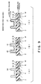
Fig.9 is a process chart for forming an HSG poly-silicon
film as a poly-silicon film whose surface has an irregular profile.
In Fig.9A, a channel stopper 2, a source 4 and a drain 6 are formed
on a surface of a semiconductor wafer W consisting of for example
a silicon wafer. On surfaces thereof, a layer insulation film
8 consisting of SiO2 is formed, which may be deposited by using
TEOS or the like. A gate electrode 10 is buried in the layer
insulation film 8 at a portion between the source 4 and the drain
6. In addition, a bit line 12 is connected to the drain 6. The
source 4 is connected to a lower electrode 14 that is formed so
as to fulfill a contact hole extending through the layer
insulation film 8. An upper end of the lower electrode 14 is
formed into a cylindrical circular shape, which enables to make
a stack capacitor. For example, the lower electrode 14 is made
of a phosphorus-doped amorphous silicon film in which phosphorus
atoms have been doped.
Then, in the semiconductor wafer W formed as shown in Fig.9A,
as shown in Fig.9B, a non-doped amorphous silicon film 16 is
selectively formed on the surface of the lower electrode 14. In
addition, by causing migration by a thermal process under a higher
vacuum, silicon-core crystal is selectively formed only on the
non-doped amorphous silicon film 16. Furthermore, as shown in
Fig.9C, the core crystal is caused to grow up by atoms in the
non-doped amorphous silicon film 16 moving. Thus, the HSG
silicon film 18 whose surface has the irregular profile is formed.
Herein, sillan or disilane is used as a process gas. A process
temperature is for example about 500 to 600 °C. Regarding a
process pressure, for example when the sillan is used, a partial
pressure is 2 × 10⁻³ Torr (2.66 × 10⁻¹ Pa) or less.
Fig.10 is a process chart for forming a rugged poly-silicon
film as a poly-silicon film whose surface has an irregular profile.
A state shown in Fig.10A is the same as that shown in Fig.9A.
From the state, as shown in Fig.10B, a rugged poly-silicon film
20 whose surface has an irregular profile is directly caused to
deposit on an entire surface of the semiconductor wafer W by a
predetermined film-forming process. In the case, the rugged
poly-silicon film 20 is deposited on the entire surface of the
wafer. After that, by a pattern etching process, as shown in
Fig.10C, the rugged poly-silicon film 20 at unnecessary portions
is removed so that the rugged poly-silicon film 20 only on the
surface of the lower electrode 14 is left.
As shown in Figs.9 and 10, after the HSG poly-silicon film
18 whose surface has the irregular profile or the rugged
poly-silicon film 20 whose surface has the irregular profile is
formed on the surface of the lower electrode 14, an annealing
process is conducted at a predetermined temperature. Thus,
phosphorus atoms diffuse from the lower electrode 14 being a lower
phosphorus-doped amorphous silicon film to the core poly- silicon
film 18 or 20. Thus, the core poly- silicon film 18 or 20 becomes
a part of the lower electrode. Therefore, the surface area of
the lower electrode 14 can be substantially enlarged because of
irregularity of the surface of poly- silicon film 18 or 20 in which
phosphorus has been doped as described above.
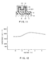
After that, as shown in Fig.11, a capacitance insulating
film 22 consisting of SiO2 or the like is formed on a surface side
of the lower electrode 14. Then, a capacitor is formed by making
a patterning-processed upper electrode 24.
Herein, in order to cause the HSG poly-silicon film 18 or
the rugged poly-silicon film 20 to sufficiently serve as the part
of the lower electrode, an enough amount of phosphorus atoms has
to be diffused and doped from the lower electrode 14 being the
lower phosphorus-doped amorphous silicon film. If the
diffusions of the phosphorus atoms are not enough, a depletion
layer may be generated, which may cause reduction of the
capacitance. A state of the case is shown in Fig.12. Fig.12 is
a graph showing a capacitance change when positive and negative
voltages are applied to the capacitor produced as described above.
As clearly seen from the graph, the capacitance remarkably reduces
when the voltage is negative, which is undesired in performance
as the capacitor.
As a measure thereto, in the case of the HSG poly-silicon
film, it may be thought to make the thickness of the film thinner.
However, if the thickness is too thin, the irregularity of the
surface of the HSG film can not appear. In addition, it may be
also thought to increase phosphorus density in the lower electrode
14. However, if the phosphorus density is too high, it becomes
difficult to form the HSG film by migration.
As another measure, ionizing phosphorus atoms and directly
implanting the ionized phosphorus atoms to the silicon film 18
or 20 with an implantation unit are carried out. However, in the
case, the silicon film 18 or 20 may be heavily damaged by the
ion implantation. In addition, in the case of the lower electrode
14 having the complicated configuration as shown in Figs.9 and
10, it is difficult for the ions to reach side wall portions
thereof. That is, it is difficult to implant the phosphorus atoms
at even ion density.
In addition, doping phosphorus atoms in the poly- silicon
film 18 or 20 is also carried out by an anneal process in a POCl3
atmosphere. However, in the case, if an annealing temperature
is not set at 800 °C or more, the phosphorus atoms are not doped
sufficiently. However, if the semiconductor wafer itself is
exposed to such a high temperature atmosphere, phosphorus density
may change in a depth direction by thermal budgets, to be out
from a designed value for a device.
SUMMARY OF THE INVENTION
This invention is intended to solve the above problems
effectively. An object of this invention is to provide a thermal
processing method that can efficiently dope phosphorus atoms into
a poly-silicon film whose surface has an irregular profile so
that a depletion layer is prevented from being generated.
This invention is a thermal processing method comprising:
a loading step of loading an object to be processed into a
processing container, the object having a surface provided with
a silicon film having a minutely irregular profile; and a doping
step of introducing phosphorus atoms in the silicon film as
impurities, by using PH3 gas as a doping gas while maintaining
a temperature of 550 to 750 °C.
By using PH3 gas as a doping gas and by setting a temperature
of the thermal process at the range of 550 to 750 °C, impurity
density (phosphorus density) may not change from a designed value
so much because the temperature is lower than 750 °C. In addition,
since the temperature is not lower than 550 °C, efficiency of
impurity doping may be maintained high to a certain extent.
Preferably, the loading step includes a step of setting
a temperature in the processing container at a temperature lower
than 400 °C when loading the object to be processed into the
processing container. Thus, generation of natural oxide films,
which may be deposited on the silicon film of the object to be
processed, can be inhibited.
Preferably, a thermal processing method further comprises
a temperature raising step of raising a temperature in the
processing container to a range of 550 to 750 °C, between the
loading step and the doping step. In the case, preferably, a
thermal processing method further comprises a step of subjecting
the object to be processed to a cycle-purge process, between the
loading step and the temperature raising step. Thus, for example,
moisture and/or gases included in a dielectric layer of the object
to be processed or the like can be discharged prior to the thermal
process. Then, during the thermal process, attachment of natural
oxide films can be prevented.
In addition, preferably, a thermal processing method
further comprises a step of supplying the doping gas into the
processing container to a predetermined pressure, between the
loading step and the temperature raising step. Thus, it can be
prevented that re-migration of the poly-silicon film is generated
and that a surface area thereof is reduced.
Preferably, the doping step includes a step of maintaining
a pressure in the processing container at a range of 100 to 400
Torr. Thus, doping efficiency of phosphorus atoms can be
improved.
In addition, preferably, a thermal processing method
further comprises a temperature lowering step of lowering the
temperature of the processing container to a predetermined
temperature while continuing to supply the doping gas and
maintaining a pressure in the processing container at a
predetermined pressure. Thus, it can be prevented that re-migration
of the poly-silicon film is generated and that a surface
area thereof is reduced.
The silicon film having the minutely irregular profile may
be an HSG poly-silicon film. Alternatively, the silicon film
having the minutely irregular profile may be a rugged poly-silicon
film.
The silicon film into which the phosphorus atoms have been
introduced by the doping step may be used as for example a portion
of an electrode of a capacitor.
BRIEF DESCRIPTION OF THE DRAWINGS
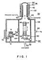
Fig.1 is a schematic view showing an example of a thermal
processing unit for carrying out a method of the invention;
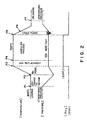
Fig.2 is a time chart for explaining a first embodiment
of a method of the invention;
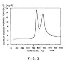
Fig.3 is a graph showing temperature-dependency of volumes
of hydrogen that has left a surface of an HSG poly-silicon film
or a rugged poly-silicon film;
Fig.4 is a graph showing temperature-dependency of volumes
of moisture that has left a surface of an SiO2 film by TEOS;
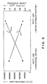
Fig.5 is a graph showing phosphorus densities and sheet
resistances in cases wherein a semiconductor wafer is loaded at
300 °C and wherein a semiconductor wafer is conventionally loaded
at 400 °C;
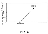
Fig.6 is a graph for evaluating effectiveness of a washing
process;
Fig.7 is a time chart for explaining a second embodiment
of a method of the invention;
Fig.8 is a graph showing ratios of capacitance;
Fig.9 is a process chart showing steps of forming an HSG
poly-silicon film as a poly-silicon film whose surface has an
irregular profile;
Fig.10 is a process chart showing steps of forming a rugged
poly-silicon film as a poly-silicon film whose surface has an
irregular profile;
Fig.11 is a view showing a capacitor having an upper
electrode that has been formed by patterning on a capacitance
insulation film; and
Fig.12 is a graph showing a capacitance change when
positive and negative voltages are applied to the capacitor.
DESCRIPTION OF THE PREFERRED EMBODIMENT
One embodiment of a thermal processing method according
to the invention is explained in detail based on attached
drawings.
Fig.1 is a schematic view showing an example of a thermal
processing unit for carrying out a method of the invention. Fig.2
is a time chart for explaining a first embodiment of a method
of the invention.
As shown in Fig.1, the thermal processing unit 30 consists
of: a longitudinal thermal processing part 32 that can conduct
a thermal process at a time to a plurality of objects to be
processed, for example a plurality of semiconductor wafers made
from silicon substrates; and a conveying part 34 that is arranged
below the thermal processing part 32 and that can convey the
semiconductor wafers W into and out from the thermal processing
part 32.
The thermal processing part 32 includes a processing
container 36 made of heat-resistant quartz. The processing
container 36 consists of an outer tube 38 whose lower end is open
but whose upper end is closed by a ceiling, and an inner tube
40 having a cylindrical shape concentrically arranged in the outer
tube 38 via a predetermined gap. A heater 42 is arranged outside
the outer tube 38, so that the entire elements form a heating
furnace. Thus, semiconductor wafers contained therein are
adapted to be heated to a predetermined temperature.
A lower side wall of the processing container 36 is provided
with a gas introduction port 44 for introducing a process gas
into the gap between the outer tube 38 and the inner tube 40,
and a discharge port 46 for sucking an atmosphere in the processing
container 36 from an inside of the inner tube 40 to create a vacuum.
About 25 to 150 pieces of the semiconductor wafers W are
supported by a wafer boat 48, which is made of for example crystal,
at substantially the same pitch in a vertical tier-like manner.
The wafer boat 48 is supported by a tip portion of the supporting
arm 52, which is moved up and down by an elevating mechanism 50
including a ball screw or the like contained in the conveying
part 34. In detail, the tip portion of the supporting arm 52 has
a disk-like cap portion 54 that can hermetically seal a lower-end
opening of the processing container 36. The wafer boat 48 is
placed on the cap portion 54 via a thermal insulating tube 56
made of for example crystal. Thus, by the elevating mechanism
50 being operated, the wafer boat 48 supporting the semiconductor
wafers W is adapted to be loaded into and unloaded from the
processing container 36 via the lower-end opening.
A wall-box 58 of the conveying part 34 is made of for example
stainless steel or the like. A side wall thereof is provided with
a gas inlet 60 for introducing an inert gas such as N2 thereinto.
A base portion thereof is provided with a gas outlet 62 for
discharging the inside atmosphere to create a vacuum.
A second elevating mechanism 64 including a ball screw or
the like is arranged in the conveying part 34. The second
elevating mechanism 64 is provided with a conveying arm 66 in
such a manner that the conveying arm can be moved up and down.
The conveying arm 66 itself can rotate, expand and retract in
a horizontal direction. A stage 68 is arranged in a vicinity of
the conveying arm 66 in such a manner that the stage 68 can be
moved up and down. A cassette 70, which can contain a plurality
of, for example about 25 semiconductor wafers W and can be
hermetically sealed, is placed on the stage 68. A side wall of
the box-wall 58 is provided with a gate door 72 for conveying
the cassette 70 into and/or from the box-wall 58.
Next, a method of the invention that can be carried out
by using the above thermal processing unit is explained.
At first, a general process of a semiconductor wafer W is
explained. As shown in Figs.9C and 10C, the semiconductor wafer
W, on which the silicon film 18 or 20 has been formed, is contained
in the tightly-closed type of cassette 70 after a natural oxide
film thereon is removed by a washing process. The cassette 70
is conveyed to the thermal processing unit 30 for an annealing
process. The cassette 70 conveyed to the thermal processing unit
30 is placed on the stage 68 in the wall-box 58 of the conveying
part 34, which has been filled with the inert atmosphere, via
the gate door 72. Then, a lid of the cassette 70 is opened by
a lid opening/closing mechanism not shown.
Then, the conveying arm 66 in the conveying part 34 is
suitably expanded, retracted, rotated and moved up or down so
that all the washed wafers W in the cassette 70 are conveyed in
turn to the wafer boat 48 that is standing by. Then, the
semiconductor wafers W are supported by the wafer boat 48 in a
tier-like manner.
If all the wafers W have been conveyed, the wafer boat 48
is moved up by the elevating mechanism 50 being operated, so that
the wafer boat 48 is inserted and loaded into the processing
container 36, which has been previously heated to the
predetermined temperature, via the lower-end opening. The
lower-end opening is hermetically sealed by the cap portion 54.
After the loading operation of the wafers W is completed
as described above, heat value supplied from the heater 42 is
increased in order to heat the wafers W and maintain the
temperature of the wafers W at a predetermined process temperature.
On the other hand, PH3 gas is supplied at a predetermined rate
from the gas introduction nozzle 44 while the atmosphere is
discharged to create a vacuum, in order to maintain an inside
pressure in the processing container 36 at a predetermined process
pressure, which is 100 to 400 Torr (13300 to 53200 Pa) in the
case. In the state, phosphorus atoms are doped in the poly-silicon
film by a thermal process i.e. an annealing process.
Then, after the predetermined thermal process is completed,
reverse operation with respect to the above operation is carried
out in order to discharge the processed semiconductor wafers W
from the conveying part 34.
Then, with reference to Fig.2, the first embodiment of the
method of the invention is explained in detail. Fig.2 shows
process temperatures, process pressures and whether PH3 gas is
supplied or not, as a timing chart.
At first, the processing container 36, which is standing
by, is in a low-temperature state not higher than 400 °C. In the
state, the wafers W are loaded (point P1). Thus, it can be
prevented that natural oxide films attach on the HSG poly-silicon
films or the rugged poly-silicon films on the surfaces of the
wafers. In the shown example, the temperature of the processing
container 36 is set at 300 °C.
Next, after the wafers W are loaded into the processing
container 36, the atmosphere in the processing container 36 is
discharged. When the atmosphere in the container is discharged
to a certain extent (point P2), N2 gas is supplied into the
processing container 36 in order to prevent attachment of the
natural oxide films. At the same time, power supplied to the
heater 42 is increased in order to raise the temperature of the
wafers W to the process temperature.
Herein, the process temperature is set to a temperature
lower than the temperature at an annealing process that is carried
out by using POCl3 (chloride phosphoryl) or the like in prior art,
for example 800°C, that is, set to a temperature in a range of
550 to 750 °C. In the shown example, the process temperature is
set to 700 °C. When the wafer temperature reaches 700°C (point
P3), supply of the N2 gas is stopped. At the same time, supply
of the PH3 gas is started. Thus, gas replacement is carried out
(point P4), then an annealing process automatically starts. In
the case, if the process temperature at the annealing process
is set to a value higher than 750°C, impurities that have already
been doped in the wafers W further diffuse and cause the
performance to deviate from a designed value. In addition, if
the process temperature is lower than 550°C, the phosphorus atoms
may not be doped into the poly-silicon film efficiently.
Therefore, if the process temperature at the annealing
process wherein the PH3 gas is used is set in the range of 550
to 750 °C, the electrical designed value of the device is kept.
In addition, the phosphorus atoms can be doped efficiently.
After the annealing process has been carried out for a
predetermined time for doping the phosphorus atoms as described
above(point P5), the supply of the PH3 gas is stopped. At the
same time, the temperature of the processing container 36 starts
to be lowered to a waiting temperature, for example 300 °C. In
addition, a cycle-purge process, wherein supplying N2 gas and
discharging the atmosphere gas are repeated in turn, is carried
out for a predetermined time (till point P6). Thus, the remaining
PH3 gas is discharged. Then, if the temperature of the processing
container 36 reaches the waiting temperature (300°C) and if the
pressure in the processing container 36 reaches the atmospheric
pressure (point P7), an unloading operation is conducted. That
is, the wafers W in which the phosphorus atoms have been doped
are taken out from the processing container 36. Thus, a series
of annealing processes are completed.
Thus, in the first embodiment, the PH3 gas is used as the
process gas. The annealing process is conducted in the range of
550 to 750 °C that is lower than 800 °C at the conventional POCl3
annealing process. Thus, phosphorus density may not change in
a depth direction of the device by the thermal budget. In addition,
the phosphorus atoms can be efficiently doped to the HSG
poly-silicon films or the rugged poly-silicon films.
In addition, when the wafers W are loaded into the
processing container 36, the processing container 36 is set to
a temperature that is not higher than 400 °C, i.e. 300 °C in the
embodiment. Thus, it can be prevented that natural oxide films
attach on the poly-silicon films on the surfaces of the wafers
W.
The above point is explained in detail. In general, an
SiO2 film made of TEOS may be broadly used as a layer insulation
film 8 (see Fig.9). However, there may be much moisture in such
a film. Then, during the annealing process and/or during certain
periods before and after the annealing process, the moisture may
go away from the SiO2 film little by little and may react with
the poly-silicon film to make a natural oxide film. On the other
hand, regarding the poly-silicon film whose surface has been
washed to remove natural oxide films thereon, hydrogen-terminal
is formed at the surface of the poly-silicon film. Thus, if the
hydrogen of the hydrogen-terminal does not go away, no natural
oxide film may attach on the surface. Thus, before the annealing
process, if the moisture or the like in the layer insulation film
8 is discharged positively under a condition wherein the hydrogen
of the hydrogen-terminal of the surface of the poly-silicon film
does not go away, it can be prevented that natural oxide films
attach on the poly-silicon film during the annealing process or
the like.
Fig.3 is a graph showing temperature-dependency of volumes
of hydrogen that has left the surface of the HSG poly-silicon
film or the rugged poly-silicon film. Fig.4 is a graph showing
temperature-dependency of volumes of moisture that has left the
surface of the SiO2 film by TEOS;
As clearly seen from Fig.3, if the temperature reaches
400 °C or higher, the volume of the leaving hydrogen is increased
sharply, and the state may become more active. Thus, if the
temperature of the poly-silicon film is set below 400 °C, it may
be seen that natural oxide films tend not to attach.
In addition, as clearly seen from Fig.4, the temperature
of the SiO2 film by TEOS reaches 270°C (about 300°C), H2O component
in the film leaves (is degassed) the most. Thus, when the wafers
are loaded, if the temperature of the processing container is
set to about 300 °C, much moisture may be squeezed from the layer
insulation film 8. Thus, during the annealing process it can be
prevented that the moisture reacts with the poly-silicon film
and that the natural oxide films attach thereon.
Herein, phosphorus densities and sheet resistances are
measured regarding a case wherein a semiconductor wafer is loaded
at 300 °C and another case wherein a semiconductor wafer is
conventionally loaded at 400 °C. The result is shown in Fig.5.
As clearly seen from Fig.5, if the wafer is loaded at 300 °C
according to the invention, the phosphorus density after the
annealing process becomes about 1.5 × 10²⁰ [atms/cm3], which is
much higher than 0.4 × 10²⁰ [atms/cm3] of the case wherein the
wafer is loaded at 400 °C. That is, it is seen that the sheet
resistance is lowered so much and the performance is better.
In addition, in the method of the invention, the washing
process for removing the natural oxide films or the like attached
on the surface of the poly-silicon film is conducted before the
annealing process. Thus, so much, during the annealing process,
the phosphorus atoms can be efficiently doped in order to raise
its density. Fig.6 is a graph for evaluating effectiveness of
the washing process. As shown in Fig.6, if the washing process
is not conducted, the phosphorus atoms can be hardly doped.
However, if the washing process is conducted, a large amount of
the phosphorus atoms can be doped to about 1.5 × 10²⁰ [atms/cm3].
That is, the effectiveness of the washing process could be
confirmed.
Next, a second embodiment of the method of the invention
is explained with reference to Fig.7. Fig.7 is a time chart for
explaining the second embodiment of the method of the invention.
Points of the second embodiment different from the first
embodiment are that leaving (degassed) component such as moisture
is sufficiently discharged by conducting a cycle-purge process
of N2 gas before the annealing process and that re-migration is
prevented by preventing the pressure in the processing container
from being lowered when the temperature of the wafers is raised
or lowered.
That is, in the second example, immediately after the
loading operation, wherein the wafers are loaded into the
processing container that is heated to 300 °C and standing by,
is completed (point P10), the cycle-purge process wherein the
supply of N2 gas and the discharge of the atmosphere gas are
repeated in turn is carried out. Thus, the leaving component
discharged from the layer insulation film 8 (see Fig.9) can be
efficiently discharged from the processing container. Thus, it
can be prevented that the natural oxide films, which may cause
trouble in doping the phosphorus atoms, attach on the poly-silicon
film.
Then, after the cycle-purge process is completed (point
P11), the supply of the PH3 gas is started to recover the pressure
in the processing container to a predetermined pressure, for
example a process pressure of about 100 to 400 Torr (13300 to
53200 Pa). After the recovery of the pressure is completed as
described above (point P12), the wafer temperature is raised to
a process temperature, for example 700 °C, while the process
pressure is maintained. In general, if the HSG poly-silicon film
or the rugged poly-silicon film is exposed to a high vacuum state
of 500 °C or more, re-migration may occur so that the surface may
be reduced to be out from the designed value. However, in the
second embodiment, differently from the first embodiment wherein
the state may temporarily be a high vacuum while heated, the PH3
gas is previously supplied in order to maintain the high pressure
of about 100 to 400 Torr while heated. Thus, it can be avoided
that the re-migration is generated.
Then, if the wafer temperature is raised to 700 °C (point
P13), an annealing process automatically starts for doping
phosphorus atoms. The annealing process is conducted for a
predetermined time. (At that time, a temperature recovering
process may be conducted just before the annealing process.) After
the annealing process is completed (point P14), the wafer
temperature is lowered. At that time, differently from the first
embodiment, the supply of the PH3 gas is continued in order to
maintain the pressure in the processing container at the range
of 100 to 400 Torr until the wafer temperature is lowered to the
waiting temperature i.e. 300 °C (point P15).
In the first embodiment, the cycle-purge process (between
point P5 and point P6) is conducted while the wafer temperature
is lowered. Thus, re-migration may be generated, and the
phosphorus atoms that have been once doped may diffuse outside,
to leave. However, in the second embodiment, the pressure in the
processing container is maintained at the relatively high
pressure i.e. about 100 to 400 Torr while the wafer temperature
is lowered. Herein, it can be avoided that the re-migration
occurs and/or the outside diffusion occurs.
Then, after the wafer temperature is sufficiently lowered
(point P15), a cycle-purge process of N2 gas is conducted (point
P6) to recover the atmospheric pressure.
In the second embodiment, as described above, the
cylce-purge process is conducted before the annealing process
in order to surely discharge the leavable components from the
TEOS layer insulation film. In addition, the re-migration is
prevented while the wafer temperature is raised or lowered. Thus,
the phosphorus atoms can be doped more efficiently, and electrical
performance can be maintained as designed.
In addition, in the respective embodiments, the process
pressure at the annealing process is maintained high i.e. at the
range of 100 to 400 Torr. However, the process pressure may be
maintained lower, for example at about 1 Torr (133 Pa).
The above embodiments are evaluated. The result is
explained with reference to Fig.8. Fig.8 is a graph showing
ratios of capacitance of a capacitor. In Fig.8, performance A
represents performance of the first embodiment (process
pressure: 100 Torr). Performance B represents performance of the
second embodiment (process pressure: 100 Torr). Performance C
represents performance of a case wherein the process pressure
is 1 Torr (other conditions are substantially the same as the
first embodiment). Performance D represents performance of a
case wherein the annealing process is not conducted. Herein, the
ratio of the capacitance (Cmin/Cmax) means a ratio of the minimum
capacitance (Cmin) with respect to the maximum capacitance (Cmax)
while applied bias voltage is changed from +1 V to -1 V.
In the performance D, the ratio of the capacitance is about
45 %. That is, changing rate is so high that the performance
is not preferable. On the other hand, in the cases of the
performances C, A and B, the ratios of the capacitance are about
70 %, about 80 % and about 96 %, respectively. That is, changing
rates are so low that the performances are preferable.
Especially, in the case of the second embodiment shown in the
performance B, the changing rate of the ratio of the capacitance
is the lowest, so that the performance is very preferable.
In the above embodiments, the poly-silicon film whose
surface has the irregular profile is formed on one electrode of
the capacitor. However, of course, the invention is not limited
to the embodiments.
The object to be processed is not limited to the
semiconductor wafer. Of course, the invention can be applied to
an LCD substrate, a glass substrate or the like.
As described above, according to the thermal processing
method of the invention, following good effects can be achieved.
At first, by using the PH3 gas as a doping gas and by setting
the temperature of the thermal process at the range of 550 to
750 °C, change of the impurity density may be prevented and doping
efficiency of the phosphorus may be maintained high. This may
generate less depletion layers and prevent the change of the
capacitance of the capacitor.
By setting the temperature in the processing container at
a temperature lower than 400 °C when loading the object to be
processed, it can be prevented that natural oxide films are
generated.
If the cycle-purge process by the inert gas is conducted
before the temperature of the object to be processed is raised,
the leaving (degassed) components such as moisture can be removed
so surely that attachment of natural oxide films can be prevented
more effectively.
By filling the inside of the processing container with the
doping gas to maintain the pressure therein at the predetermined
high pressure while the temperature of the object to be processed
is raised, it can be prevented that re-migration is generated.
If the process pressure is maintained high i.e. at a range
of about 100 to 400 Torr, doping efficiency of phosphorus atoms
can be improved more.
By maintaining the pressure in the processing container
at the predetermined process with the doping gas while the
temperature of the object to be processed is lowered, it can be
prevented that re-migration is generated.