EP1143306A2 - Developer container, developer amount detecting system, process cartridge, developing device, and image forming apparatus - Google Patents
Developer container, developer amount detecting system, process cartridge, developing device, and image forming apparatus Download PDFInfo
- Publication number
- EP1143306A2 EP1143306A2 EP01303291A EP01303291A EP1143306A2 EP 1143306 A2 EP1143306 A2 EP 1143306A2 EP 01303291 A EP01303291 A EP 01303291A EP 01303291 A EP01303291 A EP 01303291A EP 1143306 A2 EP1143306 A2 EP 1143306A2
- Authority
- EP
- European Patent Office
- Prior art keywords
- developer
- detecting
- capacitance
- detecting member
- amount
- Prior art date
- Legal status (The legal status is an assumption and is not a legal conclusion. Google has not performed a legal analysis and makes no representation as to the accuracy of the status listed.)
- Withdrawn
Links
- 238000000034 method Methods 0.000 title claims description 74
- 230000008569 process Effects 0.000 title claims description 73
- 238000001514 detection method Methods 0.000 claims abstract description 41
- 239000004020 conductor Substances 0.000 claims abstract 8
- 238000011144 upstream manufacturing Methods 0.000 claims description 2
- 238000007790 scraping Methods 0.000 claims 1
- 238000005259 measurement Methods 0.000 description 12
- 238000004140 cleaning Methods 0.000 description 9
- 238000010276 construction Methods 0.000 description 8
- 239000003990 capacitor Substances 0.000 description 6
- 238000004891 communication Methods 0.000 description 6
- 238000010586 diagram Methods 0.000 description 6
- 230000010354 integration Effects 0.000 description 6
- 238000012545 processing Methods 0.000 description 6
- 230000001105 regulatory effect Effects 0.000 description 6
- 239000011347 resin Substances 0.000 description 5
- 229920005989 resin Polymers 0.000 description 5
- 238000006243 chemical reaction Methods 0.000 description 4
- 239000000463 material Substances 0.000 description 4
- 238000012546 transfer Methods 0.000 description 4
- 239000004734 Polyphenylene sulfide Substances 0.000 description 3
- 230000001276 controlling effect Effects 0.000 description 3
- 230000006872 improvement Effects 0.000 description 3
- -1 polyethylene terephthalate Polymers 0.000 description 3
- 229920000139 polyethylene terephthalate Polymers 0.000 description 3
- 239000005020 polyethylene terephthalate Substances 0.000 description 3
- 229920000069 polyphenylene sulfide Polymers 0.000 description 3
- 102100040862 Dual specificity protein kinase CLK1 Human genes 0.000 description 2
- 101000749294 Homo sapiens Dual specificity protein kinase CLK1 Proteins 0.000 description 2
- 230000015572 biosynthetic process Effects 0.000 description 2
- 230000008878 coupling Effects 0.000 description 2
- 238000010168 coupling process Methods 0.000 description 2
- 238000005859 coupling reaction Methods 0.000 description 2
- 230000007613 environmental effect Effects 0.000 description 2
- 239000002184 metal Substances 0.000 description 2
- 239000004793 Polystyrene Substances 0.000 description 1
- 230000009471 action Effects 0.000 description 1
- 239000000853 adhesive Substances 0.000 description 1
- 230000001070 adhesive effect Effects 0.000 description 1
- 238000013019 agitation Methods 0.000 description 1
- 230000006866 deterioration Effects 0.000 description 1
- 230000000694 effects Effects 0.000 description 1
- 229920001971 elastomer Polymers 0.000 description 1
- 230000002708 enhancing effect Effects 0.000 description 1
- 230000001747 exhibiting effect Effects 0.000 description 1
- 239000004744 fabric Substances 0.000 description 1
- 238000005562 fading Methods 0.000 description 1
- 239000006261 foam material Substances 0.000 description 1
- 230000006870 function Effects 0.000 description 1
- 238000012986 modification Methods 0.000 description 1
- 230000004048 modification Effects 0.000 description 1
- 229920002223 polystyrene Polymers 0.000 description 1
- 230000009467 reduction Effects 0.000 description 1
- 239000005060 rubber Substances 0.000 description 1
- 230000035945 sensitivity Effects 0.000 description 1
- 230000007704 transition Effects 0.000 description 1
- 238000003466 welding Methods 0.000 description 1
Images




Classifications
-
- G—PHYSICS
- G03—PHOTOGRAPHY; CINEMATOGRAPHY; ANALOGOUS TECHNIQUES USING WAVES OTHER THAN OPTICAL WAVES; ELECTROGRAPHY; HOLOGRAPHY
- G03G—ELECTROGRAPHY; ELECTROPHOTOGRAPHY; MAGNETOGRAPHY
- G03G15/00—Apparatus for electrographic processes using a charge pattern
- G03G15/06—Apparatus for electrographic processes using a charge pattern for developing
- G03G15/08—Apparatus for electrographic processes using a charge pattern for developing using a solid developer, e.g. powder developer
-
- G—PHYSICS
- G03—PHOTOGRAPHY; CINEMATOGRAPHY; ANALOGOUS TECHNIQUES USING WAVES OTHER THAN OPTICAL WAVES; ELECTROGRAPHY; HOLOGRAPHY
- G03G—ELECTROGRAPHY; ELECTROPHOTOGRAPHY; MAGNETOGRAPHY
- G03G21/00—Arrangements not provided for by groups G03G13/00 - G03G19/00, e.g. cleaning, elimination of residual charge
- G03G21/16—Mechanical means for facilitating the maintenance of the apparatus, e.g. modular arrangements
- G03G21/18—Mechanical means for facilitating the maintenance of the apparatus, e.g. modular arrangements using a processing cartridge, whereby the process cartridge comprises at least two image processing means in a single unit
- G03G21/1803—Arrangements or disposition of the complete process cartridge or parts thereof
- G03G21/1814—Details of parts of process cartridge, e.g. for charging, transfer, cleaning, developing
-
- G—PHYSICS
- G03—PHOTOGRAPHY; CINEMATOGRAPHY; ANALOGOUS TECHNIQUES USING WAVES OTHER THAN OPTICAL WAVES; ELECTROGRAPHY; HOLOGRAPHY
- G03G—ELECTROGRAPHY; ELECTROPHOTOGRAPHY; MAGNETOGRAPHY
- G03G15/00—Apparatus for electrographic processes using a charge pattern
- G03G15/06—Apparatus for electrographic processes using a charge pattern for developing
- G03G15/08—Apparatus for electrographic processes using a charge pattern for developing using a solid developer, e.g. powder developer
- G03G15/0822—Arrangements for preparing, mixing, supplying or dispensing developer
- G03G15/0848—Arrangements for testing or measuring developer properties or quality, e.g. charge, size, flowability
- G03G15/0856—Detection or control means for the developer level
-
- G—PHYSICS
- G03—PHOTOGRAPHY; CINEMATOGRAPHY; ANALOGOUS TECHNIQUES USING WAVES OTHER THAN OPTICAL WAVES; ELECTROGRAPHY; HOLOGRAPHY
- G03G—ELECTROGRAPHY; ELECTROPHOTOGRAPHY; MAGNETOGRAPHY
- G03G15/00—Apparatus for electrographic processes using a charge pattern
- G03G15/06—Apparatus for electrographic processes using a charge pattern for developing
- G03G15/08—Apparatus for electrographic processes using a charge pattern for developing using a solid developer, e.g. powder developer
- G03G15/0822—Arrangements for preparing, mixing, supplying or dispensing developer
- G03G15/0848—Arrangements for testing or measuring developer properties or quality, e.g. charge, size, flowability
- G03G15/0856—Detection or control means for the developer level
- G03G15/086—Detection or control means for the developer level the level being measured by electro-magnetic means
-
- G—PHYSICS
- G03—PHOTOGRAPHY; CINEMATOGRAPHY; ANALOGOUS TECHNIQUES USING WAVES OTHER THAN OPTICAL WAVES; ELECTROGRAPHY; HOLOGRAPHY
- G03G—ELECTROGRAPHY; ELECTROPHOTOGRAPHY; MAGNETOGRAPHY
- G03G15/00—Apparatus for electrographic processes using a charge pattern
- G03G15/06—Apparatus for electrographic processes using a charge pattern for developing
- G03G15/08—Apparatus for electrographic processes using a charge pattern for developing using a solid developer, e.g. powder developer
- G03G15/0822—Arrangements for preparing, mixing, supplying or dispensing developer
- G03G15/0887—Arrangements for conveying and conditioning developer in the developing unit, e.g. agitating, removing impurities or humidity
- G03G15/0891—Arrangements for conveying and conditioning developer in the developing unit, e.g. agitating, removing impurities or humidity for conveying or circulating developer, e.g. augers
-
- G—PHYSICS
- G03—PHOTOGRAPHY; CINEMATOGRAPHY; ANALOGOUS TECHNIQUES USING WAVES OTHER THAN OPTICAL WAVES; ELECTROGRAPHY; HOLOGRAPHY
- G03G—ELECTROGRAPHY; ELECTROPHOTOGRAPHY; MAGNETOGRAPHY
- G03G2221/00—Processes not provided for by group G03G2215/00, e.g. cleaning or residual charge elimination
- G03G2221/16—Mechanical means for facilitating the maintenance of the apparatus, e.g. modular arrangements and complete machine concepts
- G03G2221/18—Cartridge systems
- G03G2221/183—Process cartridge
Definitions
- the present invention relates to an electrophotographic image forming apparatus. Further, the present invention relates to a process cartridge, a developing device, a developer amount detecting system, and a developer container.
- Examples of the electrophotographic image forming apparatus include: an electrophotographic copying machine, an electrophotographic printer (such as an LED printer and a laser beam printer), and an electrophotographic facsimile apparatus.
- a process cartridge is formed by combining at least one of charging means, developing means, and cleaning means with an electrophotographic photosensitive member to compose an integral unit in the form of a cartridge that is detachably mountable to the main body of an electrophotographic image forming apparatus, or is formed by combining at least developing means with an electrophotographic photosensitive member to compose an integral unit in the form of a cartridge that is detachably mountable to the main body of an electrophotographic image forming apparatus.
- Japanese Patent Application Laid-Open No. 5-100571 discloses a developer amount detecting device which includes, instead of two electrode bars, a developer detecting electrode member having two parallel electrodes which are arranged in parallel in the same plane at a predetermined interval and interdigitated with each other in a protrusion-and-recess-like fashion, the developer detecting electrode member being installed on the lower surface of the developer container. In this device, a variation in capacitance between the parallel electrodes arranged in a planar fashion is detected to thereby detect whether there is any developer in the container.
- Another concern of the present invention is to provide a developer container, a developing device, a process cartridge, a developer amount detecting system, and an electrophotographic image forming apparatus in which it is possible to successively detect the remaining amount of developer with high accuracy.
- the present invention further seeks to provide a developer container, a developing device, a process cartridge, a developer amount detecting system, and an electrophotographic image forming apparatus in which it is possible to successively detect the remaining amount of developer in a stable manner.
- a further concern of the present invention is to provide a developer container, a developing device, a process cartridge, a developer amount detecting system, and an electrophotographic image forming apparatus in which it is possible to successively detect the remaining amount of developer at low cost.
- a further concern of the present invention is to provide an electrophotographic image forming apparatus, a process cartridge, a developing device, a developer amount detecting system, and a developer container which are provided with low-cost, high-accuracy developer amount detecting means which makes it possible to obtain a stable detection value as the developer in the developer container is consumed and to measure the remaining amount thereof with high accuracy.
- a further object of the present invention is to provide a developer container, a developing device, a process cartridge, a developer amount detecting system, and an electrophotographic image forming apparatus comprising:
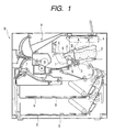
- the electrophotographic image forming apparatus is an electrophotographic laser beam printer B, which forms images on recording mediums, such as recording paper, OHP sheets, or cloth, by the electrophotographic image forming process.
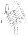
- the process cartridge A which will be described in detail below with reference to Fig. 2, is formed as an integral unit by combining the following components: a drum-shaped electrophotographic photosensitive member, i.e., a photosensitive drum 1, charging means 2 for uniformly charging the surface of the photosensitive drum 1, a roller-shaped developer bearing member opposed to the photosensitive drum 1 and serving as the developing means, i.e., a developing roller 3, a developing container D connected to the developing roller 3 and formed of a resin such as polystyrene, a developer container E serving as a developer containing portion containing developer, and a cleaning container C having cleaning means 8.
- a drum-shaped electrophotographic photosensitive member i.e., a photosensitive drum 1
- charging means 2 for uniformly charging the surface of the photosensitive drum 1
- a roller-shaped developer bearing member opposed to the photosensitive drum 1 and serving as the developing means i.e., a developing roller 3
- a developing container D connected to the developing roller 3 and formed of a resin such as poly
- the laser beam printer B serving as the image forming apparatus, there is arranged above the process cartridge A a laser scanner 4 for applying a laser beam in accordance with image information, and, below the process cartridge A, there is arranged transfer means 5 opposed to the photosensitive drum 1.
- image formation is performed as follows.
- the photosensitive drum 1 is uniformly charged by the charging means 2, and its surface is scanned and exposed by the laser beam applied from the laser scanner 4, thereby forming an electrostatic latent image of the target image information.
- the developing roller 3 By the action of the developing roller 3, some developer T in the developing container D adheres to the electrostatic latent image, which is thereby visualized.
- the developer used is an insulating magnetic monocomponent developer (toner).
- the developer is not restricted to the above-mentioned one. Any type of developer will do as long as it is a magnetic developer or an insulating magnetic developer.
- the image on the photosensitive drum 1 is transferred by the transfer means 5 to a recording sheet S fed and conveyed from a feed cassette 6.
- the recording sheet S is passed through fixing means 7, whereby the image is fixed to the recording sheet S, which is discharged onto a discharge tray 9 outside the main body.
- the developer T remaining on the photosensitive drum 1 is removed by the cleaning means 8 and collected in the cleaning container C.
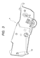
- a memory unit 100 serving as storage means is mounted in the process cartridge A.
- the memory unit 100 is attached to a side surface of the process cartridge A.
- an engine controller 50 for performing system control on the entire image forming apparatus, and a central processing unit (CPU) (not shown) is arranged inside the engine controller 50. A series of system processing operations are conducted in accordance with a program previously stored in the central processing unit.
- CPU central processing unit
- a high-voltage power supply 51 generates a charging bias which is to be supplied to the charging means 2 and which consists of a DC voltage and an AC voltage superimposed thereon, a developing bias which is to be supplied to the developing roller 3 and which consists of a DC voltage and an AC voltage superimposed thereon, a transfer bias which is a DC voltage to be supplied to the transfer means 5, and a fixing bias which is a DC voltage to be supplied to the fixing means 7.
- a driving portion 52 including a motor, solenoid, etc. provided inside the apparatus, a sensor group 53 provided at a predetermined position in the image forming apparatus, an indicating portion 54 for indicating the condition of the apparatus, and first and second developer amount detecting devices 55A and 55B adapted to detect the capacitance of a developer detecting member in the process cartridge A to thereby detect the developer amount, the above-mentioned components being controlled by the engine controller 50.
- a memory controlling circuit 56 for controlling the memory unit 100 mounted in the process cartridge.
- the memory unit 100 which, in this embodiment, is attached to a side surface of the process cartridge A, as shown in Fig. 3.
- the memory unit 100 contains a nonvolatile built-in storage element, and is capable of writing and reading data by performing data communication with the image forming apparatus main body.
- the control of the data communication is all effected by the memory controlling circuit 56.
- the data communication is effected in a non-contact manner through magnetic coupling between an antenna provided in the memory unit 100 and an antenna provided in the image forming apparatus main body.
- the antenna of the memory unit 100 is brought close to the antenna provided in the laser printer B, whereby communication is possible.
- a power supply circuit is provided in the memory unit 100; all the DC power used in the apparatus is supplied from this power supply circuit. In the power supply circuit, an electric current generated in the antennas through the magnetic coupling of the two antennas is rectified, thereby generating a DC voltage.
- information on the process cartridge A, etc. is stored.
- Fig. 2 is an exploded perspective view of the process cartridge A of this embodiment
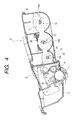
- Fig. 4 is a sectional view of the process cartridge A.
- the process cartridge A of this embodiment has a developer container E containing developer, a developing container D for retaining the developing roller 3 serving as the developing member, a cleaning container C retaining the photosensitive drum 1 and the cleaning means 8, and side covers 10 and 11 retaining the developer container E and the cleaning container C, the containers being connected together to form a cartridge.
- the developer container E has a horizontally elongated configuration to meet the demand for an increase in capacity, and the bottom surface of the developer container E exhibits three recesses.
- Three conveying members 12, 13, and 14 driven by a main body motor (not shown) are in correspondence with the recesses of the developer container E, and developer T is conveyed to the developing container D by agitating wing members 12a, 13a, and 14a provided on the conveying members 12, 13, and 14.
- the self-weight of the developer T is relieved, so that it is possible to mitigate fading, a deterioration in the developer, an increase in agitation torque, etc.
- the agitating wing members 12a through 14a are formed of a resin sheet material such as polyethylene terephthalate, polyphenylene sulfide or the like, and are adapted to agitate and convey the developer T.
- the rotation radius o:E the distal ends of the agitating wing members 12a through 14a is larger than the radius of the recesses of the bottom surface of the developer container E, and the distal ends rub against the bottom surface of the developer container E, whereby the developer T is horizontally conveyed, without leaving any developer T on the bottom surface of the developer container E.
- a first detecting member 20 and a second detecting member 21 are provided.
- the first detecting member 20 performs detection in the region in which the amount of developer T is relatively large
- the second detecting member 21 performs detection in the region in which the amount of developer T is relatively small.
- the first detecting member 20 performs detection from the initial stage of use to the stage at which the developer amount is reduced to approximately 50 to 10%
- the second detecting member 21 performs detection from the stage at which the developer amount is approximately 50 to 10% to the stage at which there is no developer left. Both the first detecting member 20 and the second detecting member 21 perform developer amount measurement based on capacitance.
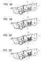
- Figs. 5A, 5B, 5C, and 5D show how the developer amount varies
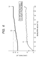
- Fig. 6 shows the relationship between developer amount and capacitance.
- transition from the first detecting member 20 to the second detecting member 21 is effected when the developer amount has been reduced to approximately 20%.
- Figs. 5A, 5B, 5C, and 5D are respectively in correspondence with points (a), (b), (c), and (d) in Fig. 6.
- the developer amount is 100%, and both the first detecting member 20 and the second detecting member 21 are buried in developer (Fig 5A). At this time, the output of the first detecting member 20 is X2.
- the amount of the portion of the developer which is in the detection region for the first detecting member 20 varies as the developer is gradually consumed (Fig. 5B).
- the output of the detecting member varies.
- the output of the first detecting member 20 is X3.
- the developer amount is reduced to approximately 20%, and the second detecting member 21 starts to operate (Fig. 5C). At this time, the output of the second detecting member 21 is Y2.
- Fig. 7 shows the first detecting member 20.
- Fig. 8 is a view of the first detecting member 20 as seen from the side opposite to that of Fig. 7, and Fig. 9 is a developed view of the first detecting member 20.
- the first detecting member 20 has a measurement-side output electrode 22a, a reference-side output electrode 22c, and a common input electrode 22b.
- a combination of the measurement-side output electrode 22a and the common input electrode 22b serves as a measurement electrode 20a
- a combination of the reference-side output electrode 22c and the common input electrode 22b serves as a reference electrode 20b.
- the measurement electrode 20a is arranged at a position inside the developer container E where it comes into contact with the developer T, for example, a position on the inner side surface of the container.
- the electrodes 22a and 22b which constitute a pair, it is possible to detect a variation in the area of the portion of the developer which is in contact with the electrode surface, thereby making it possible to ascertain the amount of developer in the developer container E. That is, since the dielectric constant of the developer T is larger than that of air, a variation in the area of the portion of the developer T which is in contact with the surface of the first detecting member 20 results in a variation in the capacitance between the electrodes 22a and 22b.
- the reference electrode 20b is arranged inside the developer container E at a position where the reference electrode 20b is out of contact with the developer T. It is designed to exhibit a variation in capacitance similar to that of the measurement electrode 20a when the environmental condition is varied.
- the measurement electrode 20a and the reference electrode 20b have the same electrode pattern configuration.
- the first detecting member 20 is preferably formed by providing the measurement electrode 20a and the reference electrode 20b on one side of a flexible board, such as a flexible print board, which is folded and arranged inside the developer container E.
- a flexible board such as a flexible print board
- the edges or the entire back surface of the first detecting member 20 is fastened to the developer container E by using an adhesive double coated tape or the like so that none of the developer may be allowed to get behind the measurement electrode 20a.
- Fig. 10 is a perspective view of the developer container E, which is provided with the three conveying members 12, 13, and 14.
- the first detecting member 20 is positioned in the region where the conveying member 13, which is the second conveying member as counted from the developing roller 3 side, is arranged, and the developer T that has reached this region is conveyed to the acting region for the second detecting member 21 described below.
- the first detecting member 20 is arranged in the developer container E at a position on the upstream side of the second detecting member 21 in the developer supplying direction, i.e., the direction in which the developer T contained in the container E is supplied toward the developing roller 3.
- the first detecting member 20 is arranged on the driving-side side wall of the developer container E so as to surround the shaft of the conveying member 13. By arranging the first detecting member 20 at this position, it is possible to reduce the area of the first detecting member 20 while realizing successive detection, so that it is possible to achieve a reduction in parts cost. Further, by positioning the first detecting member so as to be spaced apart from the developing roller 3, it is possible to minimize the influence of the developing bias.
- the first detecting member 20 exhibits very high sensitivity in the vicinity of the surface thereof, so that it is effective, in enhancing the detection accuracy, to provide a surface wiping member 13b as means for removing any developer on the surface of the detecting member. In doing so, it is desirable to provide the wiping member 13b on the developer conveying member 13 to thereby simplify the structure. Further, in this case, the first detecting member 20 is arranged in the function range for the wiping member 13b, which is in correspondence with the developer agitating region.
- the surface wiping member 13b for the first detecting member 20 is provided on the developer conveying member 13.
- the wiping member 13b is provided only on the conveying member 13, which is at the position where the first detecting member 20 is provided.
- the developer conveying member 13 includes an agitating rod member 13c, an agitating wing member 13a, an agitating wing holding member 13d, and the wiping member 13b.
- the agitating rod member 13c is rotatably supported by the developer container E.
- the agitating wing member 13a is pressed against the agitating rod member 13c and fastened thereto by the agitating wing holding member 13d.
- the agitating wing holding member 13d is formed of sheet metal or resin and secured to the agitating rod member 13c by heat caulking, ultrasonic welding, adhesion or the like.
- the wiping member 13b is secured in position by the agitating wing holding member 13d.
- the agitating wing member 13a is formed of a resin material, such as polyethylene terephthalate or polyphenylene sulfide.
- the wiping member 13b may be formed of a resin sheet material such as polyethylene terephthalate or polyphenylene sulfide, rubber or foam material. That is, an arbitrary material can be employed for the wiping member 13b as long as it is suitable for wiping of the surface of the first detecting member 20.
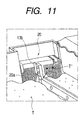
- Fig. 11 shows the first detecting member 20 in a state in which the developer has been consumed to some extent. In this state, there exists adhering developer T' above the developer surface. The presence of the adhering developer T' leads to an increase in the capacitance of the measurement electrode 20a of the first detecting member 20, resulting in discrepancies.
- the first detecting member 20 serving as the first capacitance generating member is connected to the first developer amount detecting device 55A shown in Fig. 14, where the capacitance of the first detecting member 20 is detected.
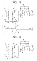
- Fig. 15 is a diagram showing the inner circuit configuration of the developer amount detecting device 55A.
- a terminal 59 is connected to the electrode 22b of the first detecting member 20 via an electric contact (not shown) whose contact portion is exposed through the cartridge frame, and is adapted to output a clock CLK1 for detecting developer amount.
- the clock CLK1 is generated by resistors 62 and 63 and a transistor 64.
- a signal CLKA is a clock output from the engine controller 50, and is a rectangular wave having a frequency fc of 50 KHz and a duty of 50%.
- the signal CLKA is amplified to an amplitude of Vc by the transistor 64 and output from the terminal 59.
- a terminal 57 is connected to the measurement-side output electrode 22a of the first detecting member 20 via an electric contact (not shown) whose contact portion is exposed through the cartridge frame.
- an AC current I12 flows through the terminal 57 due to the capacitance Ct between the electrodes 22a and 22b.
- the magnitude of the AC current I12 is of a value corresponding to the value of the capacitance Ct.
- the AC current I12 is rectified by diodes 69 and 67 provided in the input portion of the terminal 57, and a current I13 obtained through the rectification is input to an integration circuit formed by an operation amplifier 72, a resistor 75, and a capacitor 76.
- the current I13 is a current corresponding to a one-direction component (hereinafter referred to as "half-wave current”) of the current I12.
- a terminal 58 is connected to the reference-side output electrode 22c of the first detecting member 20 through an electric contact (not shown) whose contact portion is exposed through the cartridge frame. Due to the clock output from the terminal 59, an electric current I14 of a magnitude corresponding to the capacitance Cr between the electrode 22b and the electrode 22c flows through the terminal 58.
- the electric current I14 is rectified by diodes 68 and 70 set to a direction opposite to the input portion of the terminal 57, and an electric current I15 is input to the integration circuit.
- the electric current I15 is a half-wave current of a polarity opposite to that of the electric current I13.
- Vd1 Rs1 ⁇ fc ⁇ Vc ⁇ (Ct - Cr)
- a reference voltage Vt1 is input from the power supply 71 to the positive input terminal of the operation amplifier 72, and the output voltage Vs1 of the operation amplifier 72 has a characteristic that can be expressed by the following equation.
- Vs1 Vt1 - Rs1 ⁇ fc ⁇ Vc ⁇ (Ct - Cr)
- the output voltage Vs1 of the operation amplifier 72 is the difference between the capacitance between the electrodes 22a and 22b on the measurement electrode 20a side and the capacitance between the electrodes 22c and 22b on the reference electrode 20b side, that is, a voltage value according to the amount of developer in the process cartridge A.
- the output Vs1 of the operation amplifier is output from an output terminal 60.
- the terminal 60 is connected to the analog-digital conversion terminal of the central processing unit in the engine controller 50.
- the voltage level Vs1 which is in correspondence with the developer amount, is converted to digital data, and is compared with a conversion table previously stored in the engine controller 50, whereby it is converted to the developer amount T1 in the process cartridge A.
- Fig. 12 is a, sectional view of the developer container E
- Fig. 13 is a perspective view as seen from below of the developer container E.
- the second detecting member 21 is provided outside the developer container E. Further, a cover member 23 is provided on the outer side of the second detecting member 21.
- the second detecting member 21 is formed of sheet metal, and extends over the entire longitudinal range so as to be in conformity with the outside protruding configuration according to the inside recess of the bottom surface of the developer container E.
- the developing roller 3 and the developer regulating member supporting member 15 are electrically connected to each other, and a variation in the capacitance between the second detecting member 21, the developing roller 3, and the developer regulating member supporting member 15 is measured, whereby the developer amount is detected.
- the second detecting member 21 is outside the developer container E, and is fastened to the protrusion of the developer container E which is nearest to the developing roller 3 by caulking, adhesion or the like.
- the second detecting member 21 as the second capacitance generating portion is connected to the second developer amount detecting device 55B of Fig. 14, and the value of capacitance between the second detecting member 21, the developing roller 3, and the developer regulating member supporting member 15 is detected.
- Fig. 16 is an inner circuit diagram of the second developer amount detecting device 55B.
- a terminal 80 is connected to the second detecting member 21 via an electric contact (not shown).
- an AC current I1 flows through the terminal 80 due to the capacitance Cs between the second detecting member 21, the developing roller 3, and the developer regulating member supporting member 15.
- the magnitude of the current I1 is of a value corresponding to the capacitance value Cs.
- the electric current I1 is rectified by diodes 86 and 88 provided in the input portion of the terminal 80, and an electric current I2 obtained through the rectification is input to an integration circuit formed by an operation amplifier 91, a resistor 93, and a capacitor 94.
- the electric current I2 is a half-wave current of the electric current I1.
- a terminal 81 is connected to a developing bias output portion (not shown) in the high-voltage power supply 51. That is, the same developing bias as that of the developing roller 3 is applied to the terminal 81.
- a capacitor 85 of a capacitance Ck is connected to the input portion of the terminal 81. When a developing AC bias is applied thereto, an AC current I3 of a magnitude corresponding to the capacitance Ck flows.
- the capacitor 85 is a reference capacitor serving as a measurement reference, and its capacitance value Ck is set to the value of the capacitance between the second detecting member 21, the developing roller 3, and the developer regulating member supporting-member 15 when there is no developer in the process cartridge A.
- the electric current I3 is rectified by diodes 87 and 89 set to a direction opposite to the input portion of the terminal 80, and an electric current I4 is input to the integration circuit.
- the electric current I4 is a half-wave current of a polarity opposite to that of the electric current I2.
- Vd2 a DC voltage corresponding to the average value of the sum total of the electric currents I2 and I4 is generated across the resistor 93.
- Vd2 the frequency and amplitude of the developing AC bias is fd and VP, and that the resistance value of the resistor 93 is Rs2
- Vd2 can be approximated by the following equation.
- Vd2 Rs2 ⁇ fd ⁇ Vp ⁇ (Cs - Ck)
- a predetermined reference voltage Vt2 is input from the power supply 90 to the positive input terminal of the operation amplifier 91, and the output of the operation amplifier 91 has a characteristic that can be expressed by the following equation.
- Vs2 Vt2 - Rs2 ⁇ fd ⁇ Vp ⁇ (Cs - Ck)
- the output voltage Vs2 of the operation amplifier is a voltage value corresponding to the difference between the capacitance between the second detecting member 21, the developing roller 3, and the developer regulating member supporting member 15 and the capacitance of the reference capacitor 85, that is, a voltage value corresponding to the developer amount in the process cartridge A.
- the output Vs2 of the operation amplifier 91 is output from an output terminal 82.
- the output terminal 82 is connected to an analog-digital conversion terminal of the central processing unit in the engine controller 50.
- the voltage level Vs2 corresponding to the developer amount is converted to digital data, and is compared with a conversion table previously stored in the engine controller 50 to be thereby converted to the developer amount T2 in the process cartridge A.
- the developer amount T1 detected by the first detecting member 20 and the developer amount T2 detected by the second detecting member 21 are compared with each other in the engine controller 50, and the value of the developer amount T1 or that of the developer amount T2 is indicated through an indicating portion 54 to inform the user of the value. Further, the detection value of the detected developer amount is stored in the process cartridge memory unit 100.
- the indicating portion 54 may be a display provided on the image processing apparatus main body or the display of a personal computer capable of communication by a communication means provided in the image forming apparatus main body.
- the developer container E and the developer amount detecting system described in connection with the first embodiment of the present invention are also applicable to a developing device having a developer bearing member, a developer container, etc. and adapted to develop an electrostatic latent image formed on an electrophotographic photosensitive member, making it possible to achieve the same effect as that of the first embodiment.
- the second detecting member is arranged so as to extend along the developer container such that a part of the operating region of the developer conveying member nearest to the developer bearing member is placed between the second detecting member and the developer bearing member, whereby the second detecting member is enabled to ascertain the developer amount at a point in time well before the moment when image formation becomes impossible, i.e., when there is a sufficient amount of developer left. Further, since it is arranged along the developer container, the second detecting member does not hinder the supply of developer to the developing roller.
- the first detecting member is provided on a surface of the developer container and in the operating region for the developer removing member, whereby it is possible to obtain an output exhibiting linearity to some extent as the developer amount varies. And, by providing the first detecting member in the operating region for the developer removing member, it is possible to remove any developer adhering to a portion above the developer surface, thereby achieving an improvement in terms of accuracy.
- the developer removing member is attached to the developer conveying member so as to be in contact with the surface of the first detecting member to wipe off any developer from the surface of the first detecting member
- the first detecting member is provided around the developer conveying member which is at the position where the developer is conveyed from the acting region for the first detecting member to the acting region for the second detecting member, whereby the variation in the developer amount in the acting region for the second detecting member starts substantially simultaneously with the ending of the variation in the developer amount in the detecting region for the first detecting member, thereby making it possible to perform developer amount detection without interruption.
Landscapes
- Physics & Mathematics (AREA)
- General Physics & Mathematics (AREA)
- Engineering & Computer Science (AREA)
- Computer Vision & Pattern Recognition (AREA)
- Dry Development In Electrophotography (AREA)
- Electrophotography Configuration And Component (AREA)
- Measurement Of Levels Of Liquids Or Fluent Solid Materials (AREA)
Abstract
Description
- The present invention relates to an electrophotographic image forming apparatus. Further, the present invention relates to a process cartridge, a developing device, a developer amount detecting system, and a developer container.
- Examples of the electrophotographic image forming apparatus include: an electrophotographic copying machine, an electrophotographic printer (such as an LED printer and a laser beam printer), and an electrophotographic facsimile apparatus. A process cartridge is formed by combining at least one of charging means, developing means, and cleaning means with an electrophotographic photosensitive member to compose an integral unit in the form of a cartridge that is detachably mountable to the main body of an electrophotographic image forming apparatus, or is formed by combining at least developing means with an electrophotographic photosensitive member to compose an integral unit in the form of a cartridge that is detachably mountable to the main body of an electrophotographic image forming apparatus.
- Conventionally, in electrophotographic image forming apparatuses using the electrophotographic image forming process, a process cartridge system has been widely adopted, in which an electrophotographic photosensitive member and process means acting thereon are combined into an integral unit in the form of a cartridge, which is detachably mountable to the main body of the image forming apparatus. In such a process-cartridge-type electrophotographic image forming apparatus, the user can replace the cartridge in person. In view of this, in some electrophotographic image forming apparatuses of this type, there is provided means for informing the user of consumption of the developer.
- In a conventional developer amount detecting device, two electrode bars are provided inside the developer container of developing means, and a variation in capacitance between the two electrode bars is detected to thereby detect whether there is any developer in the container. Japanese Patent Application Laid-Open No. 5-100571 discloses a developer amount detecting device which includes, instead of two electrode bars, a developer detecting electrode member having two parallel electrodes which are arranged in parallel in the same plane at a predetermined interval and interdigitated with each other in a protrusion-and-recess-like fashion, the developer detecting electrode member being installed on the lower surface of the developer container. In this device, a variation in capacitance between the parallel electrodes arranged in a planar fashion is detected to thereby detect whether there is any developer in the container.
- If it is possible to successively detect the remaining amount of developer in the developer container, the user will be advantageously enabled to see to what extent the developer has been consumed.
- It is a concern of the present invention to provide a developer container, a developing device, a process cartridge, a developer amount detecting system, and an electrophotographic image forming apparatus in which it is possible to successively detect the remaining amount of developer.
- Another concern of the present invention is to provide a developer container, a developing device, a process cartridge, a developer amount detecting system, and an electrophotographic image forming apparatus in which it is possible to successively detect the remaining amount of developer with high accuracy.
- The present invention further seeks to provide a developer container, a developing device, a process cartridge, a developer amount detecting system, and an electrophotographic image forming apparatus in which it is possible to successively detect the remaining amount of developer in a stable manner.
- A further concern of the present invention is to provide a developer container, a developing device, a process cartridge, a developer amount detecting system, and an electrophotographic image forming apparatus in which it is possible to successively detect the remaining amount of developer at low cost.
- A further concern of the present invention is to provide an electrophotographic image forming apparatus, a process cartridge, a developing device, a developer amount detecting system, and a developer container which are provided with low-cost, high-accuracy developer amount detecting means which makes it possible to obtain a stable detection value as the developer in the developer container is consumed and to measure the remaining amount thereof with high accuracy.
- A further object of the present invention is to provide a developer container, a developing device, a process cartridge, a developer amount detecting system, and an electrophotographic image forming apparatus comprising:
- (a) a first detecting member which is an electrode member having input-side and output-side electrodes formed in parallel in the same plane at a predetermined interval and adapted to detect capacitance between the electrodes and which has a measurement-side electrode that is in contact with developer and a reference electrode that is out of contact with developer;
- (b) a developer removing member for removing developer adhering to a detection region of the first detecting member; and
- (c) a second detecting member consisting of a conductive member and adapted to detect capacitance between it and a developer bearing member, wherein the first detecting member detects the developer amount partway from the start of use of the developer container, and then the second detecting member detects the developer amount.
-
- These and other features and advantages of the present invention will become more apparent upon consideration of the following description of the preferred embodiments of the present invention taken in conjunction with the accompanying drawings.
-
- Fig. 1 is a schematic sectional view showing the construction of an electrophotographic image forming apparatus according to the present invention;
- Fig. 2 is an exploded perspective view showing the construction of a process cartridge according to the present invention;
- Fig. 3 is a side view of the process cartridge of the present invention, illustrating the arrangement of a memory unit;
- Fig. 4 is a sectional view of the process cartridge of the present invention;
- Figs. 5A, 5B, 5C, and 5D are sectional views of a developer container, showing how developer is consumed;
- Fig. 6 is a graph showing the relationship between developer amount and capacitance in a developer amount detecting device according to the present invention;
- Fig. 7 is a perspective view of a first detecting member of the present invention;
- Fig. 8 is a perspective view of the first detecting member of the present invention;
- Fig. 9 is a developed view of the first detecting member of the present invention;
- Fig. 10 is a perspective view of a developer container according to the present invention;
- Fig. 11 is a perspective view showing how a wiping member of the present invention operates;
- Fig. 12 is a sectional view of the process cartridge, illustrating a second detecting member of the present invention;
- Fig. 13 is a perspective view as seen from below of the process cartridge, illustrating where the second detecting member of the present invention is arranged;
- Fig. 14 is a system block diagram showing an image forming apparatus according to the present invention;
- Fig. 15 is an inner circuit diagram of a first developer amount detecting device in the present invention; and
- Fig. 16 is an inner circuit diagram of a second developer amount detecting device in the present invention.
-
- An electrophotographic image forming apparatus, a process cartridge, a developing device, a developer amount detecting system, and a developer container according to the present invention will now be described in detail with reference to the drawings.
- A process cartridge and an electrophotographic image forming apparatus according to the present invention will now be described in detail with reference to the drawings.
- First, with reference to Fig. 1, an embodiment of an electrophotographic image forming apparatus to which a process cartridge A constructed according to the present invention can be attached will be described. In this embodiment:, the electrophotographic image forming apparatus is an electrophotographic laser beam printer B, which forms images on recording mediums, such as recording paper, OHP sheets, or cloth, by the electrophotographic image forming process.
- The process cartridge A, which will be described in detail below with reference to Fig. 2, is formed as an integral unit by combining the following components: a drum-shaped electrophotographic photosensitive member, i.e., a photosensitive drum 1, charging means 2 for uniformly charging the surface of the photosensitive drum 1, a roller-shaped developer bearing member opposed to the photosensitive drum 1 and serving as the developing means, i.e., a developing
roller 3, a developing container D connected to the developingroller 3 and formed of a resin such as polystyrene, a developer container E serving as a developer containing portion containing developer, and a cleaning container C having cleaning means 8. - In the laser beam printer B, serving as the image forming apparatus, there is arranged above the process cartridge A a laser scanner 4 for applying a laser beam in accordance with image information, and, below the process cartridge A, there is arranged transfer means 5 opposed to the photosensitive drum 1. In the image forming apparatus constructed as described above, image formation is performed as follows.
- First, the photosensitive drum 1 is uniformly charged by the
charging means 2, and its surface is scanned and exposed by the laser beam applied from the laser scanner 4, thereby forming an electrostatic latent image of the target image information. By the action of the developingroller 3, some developer T in the developing container D adheres to the electrostatic latent image, which is thereby visualized. In this embodiment, the developer used is an insulating magnetic monocomponent developer (toner). The developer is not restricted to the above-mentioned one. Any type of developer will do as long as it is a magnetic developer or an insulating magnetic developer. - The image on the photosensitive drum 1 is transferred by the transfer means 5 to a recording sheet S fed and conveyed from a
feed cassette 6. The recording sheet S is passed through fixing means 7, whereby the image is fixed to the recording sheet S, which is discharged onto adischarge tray 9 outside the main body. After the developer image has been transferred to the recording sheet S, the developer T remaining on the photosensitive drum 1 is removed by the cleaning means 8 and collected in the cleaning container C. - Further, as shown in Fig. 3, a
memory unit 100 serving as storage means is mounted in the process cartridge A. In this embodiment, thememory unit 100 is attached to a side surface of the process cartridge A. - Next, the system configuration of the image forming apparatus of this embodiment will be described with reference to the system block diagram of Fig. 14.
- There is provided an
engine controller 50 for performing system control on the entire image forming apparatus, and a central processing unit (CPU) (not shown) is arranged inside theengine controller 50. A series of system processing operations are conducted in accordance with a program previously stored in the central processing unit. - A high-
voltage power supply 51 generates a charging bias which is to be supplied to the charging means 2 and which consists of a DC voltage and an AC voltage superimposed thereon, a developing bias which is to be supplied to the developingroller 3 and which consists of a DC voltage and an AC voltage superimposed thereon, a transfer bias which is a DC voltage to be supplied to the transfer means 5, and a fixing bias which is a DC voltage to be supplied to the fixing means 7. - Further, in the system configuration of this embodiment, there are provided a driving
portion 52 including a motor, solenoid, etc. provided inside the apparatus, asensor group 53 provided at a predetermined position in the image forming apparatus, an indicatingportion 54 for indicating the condition of the apparatus, and first and second developeramount detecting devices engine controller 50. Further, connected to theengine controller 50 is amemory controlling circuit 56 for controlling thememory unit 100 mounted in the process cartridge. - Here, the
memory unit 100 will be described, which, in this embodiment, is attached to a side surface of the process cartridge A, as shown in Fig. 3. - The
memory unit 100 contains a nonvolatile built-in storage element, and is capable of writing and reading data by performing data communication with the image forming apparatus main body. The control of the data communication is all effected by thememory controlling circuit 56. The data communication is effected in a non-contact manner through magnetic coupling between an antenna provided in thememory unit 100 and an antenna provided in the image forming apparatus main body. When the process cartridge A is mounted to the laser printer B, the antenna of thememory unit 100 is brought close to the antenna provided in the laser printer B, whereby communication is possible. Further, a power supply circuit is provided in thememory unit 100; all the DC power used in the apparatus is supplied from this power supply circuit. In the power supply circuit, an electric current generated in the antennas through the magnetic coupling of the two antennas is rectified, thereby generating a DC voltage. In thememory unit 100, information on the process cartridge A, etc. is stored. - Fig. 2 is an exploded perspective view of the process cartridge A of this embodiment, and Fig. 4 is a sectional view of the process cartridge A.
- In Fig. 2, the process cartridge A of this embodiment has a developer container E containing developer, a developing container D for retaining the developing
roller 3 serving as the developing member, a cleaning container C retaining the photosensitive drum 1 and the cleaning means 8, and side covers 10 and 11 retaining the developer container E and the cleaning container C, the containers being connected together to form a cartridge. - In Fig. 4, the developer container E has a horizontally elongated configuration to meet the demand for an increase in capacity, and the bottom surface of the developer container E exhibits three recesses. Three conveying
members wing members members - Due to the horizontally elongated configuration of the developer container E, the self-weight of the developer T is relieved, so that it is possible to mitigate fading, a deterioration in the developer, an increase in agitation torque, etc.
- The agitating
wing members 12a through 14a are formed of a resin sheet material such as polyethylene terephthalate, polyphenylene sulfide or the like, and are adapted to agitate and convey the developer T. The rotation radius o:E the distal ends of the agitatingwing members 12a through 14a is larger than the radius of the recesses of the bottom surface of the developer container E, and the distal ends rub against the bottom surface of the developer container E, whereby the developer T is horizontally conveyed, without leaving any developer T on the bottom surface of the developer container E. - As shown in Fig. 4, in this embodiment, to successively detect the developer amount, a first detecting
member 20 and a second detectingmember 21 are provided. The first detectingmember 20 performs detection in the region in which the amount of developer T is relatively large, and the second detectingmember 21 performs detection in the region in which the amount of developer T is relatively small. - More specifically, the first detecting
member 20 performs detection from the initial stage of use to the stage at which the developer amount is reduced to approximately 50 to 10%, and the second detectingmember 21 performs detection from the stage at which the developer amount is approximately 50 to 10% to the stage at which there is no developer left. Both the first detectingmember 20 and the second detectingmember 21 perform developer amount measurement based on capacitance. - Figs. 5A, 5B, 5C, and 5D show how the developer amount varies, and Fig. 6 shows the relationship between developer amount and capacitance. In this embodiment, transition from the first detecting
member 20 to the second detectingmember 21 is effected when the developer amount has been reduced to approximately 20%. Figs. 5A, 5B, 5C, and 5D are respectively in correspondence with points (a), (b), (c), and (d) in Fig. 6. - At the stage corresponding to point (a), the developer amount is 100%, and both the first detecting
member 20 and the second detectingmember 21 are buried in developer (Fig 5A). At this time, the output of the first detectingmember 20 is X2. - At the stage corresponding to point (b), the amount of the portion of the developer which is in the detection region for the first detecting
member 20 varies as the developer is gradually consumed (Fig. 5B). As the area of the portion of the developer which is in contact with the surface of the first detectingmember 20 varies, the output of the detecting member varies. At this time, the output of the first detectingmember 20 is X3. - At the stage corresponding to point (c), the developer amount is reduced to approximately 20%, and the second detecting
member 21 starts to operate (Fig. 5C). At this time, the output of the second detectingmember 21 is Y2. - At the stage corresponding to point (d), detection is continued until the developer amount becomes 0% (Fig. 5D). At this time, the output of the second detecting
member 21 is Y1. Thus, detection can be successively effected over the entire range from the initial to the last stage of use of the process cartridge A. - Next, the operating principle of the first and second detecting
members member 20. Fig. 8 is a view of the first detectingmember 20 as seen from the side opposite to that of Fig. 7, and Fig. 9 is a developed view of the first detectingmember 20. In Fig. 9, the first detectingmember 20 has a measurement-side output electrode 22a, a reference-side output electrode 22c, and acommon input electrode 22b. A combination of the measurement-side output electrode 22a and thecommon input electrode 22b serves as ameasurement electrode 20a, and a combination of the reference-side output electrode 22c and thecommon input electrode 22b serves as areference electrode 20b. - In Figs. 7 and 8, the
measurement electrode 20a is arranged at a position inside the developer container E where it comes into contact with the developer T, for example, a position on the inner side surface of the container. By measuring the capacitance between theelectrodes member 20 results in a variation in the capacitance between theelectrodes - The
reference electrode 20b is arranged inside the developer container E at a position where thereference electrode 20b is out of contact with the developer T. It is designed to exhibit a variation in capacitance similar to that of themeasurement electrode 20a when the environmental condition is varied. In this embodiment, themeasurement electrode 20a and thereference electrode 20b have the same electrode pattern configuration. Thus, by subtracting the value of the capacitance of thereference electrode 20b from the value of the capacitance of themeasurement electrode 20a, it is possible to assume that there is no variation in capacitance due to the environmental condition, thereby making it possible to achieve an improvement in detection accuracy. - As shown in Fig. 9, the first detecting
member 20 is preferably formed by providing themeasurement electrode 20a and thereference electrode 20b on one side of a flexible board, such as a flexible print board, which is folded and arranged inside the developer container E. The edges or the entire back surface of the first detectingmember 20 is fastened to the developer container E by using an adhesive double coated tape or the like so that none of the developer may be allowed to get behind themeasurement electrode 20a. - Fig. 10 is a perspective view of the developer container E, which is provided with the three conveying
members member 20 is positioned in the region where the conveyingmember 13, which is the second conveying member as counted from the developingroller 3 side, is arranged, and the developer T that has reached this region is conveyed to the acting region for the second detectingmember 21 described below. - That is, in this embodiment, the first detecting
member 20 is arranged in the developer container E at a position on the upstream side of the second detectingmember 21 in the developer supplying direction, i.e., the direction in which the developer T contained in the container E is supplied toward the developingroller 3. - Further, the first detecting
member 20 is arranged on the driving-side side wall of the developer container E so as to surround the shaft of the conveyingmember 13. By arranging the first detectingmember 20 at this position, it is possible to reduce the area of the first detectingmember 20 while realizing successive detection, so that it is possible to achieve a reduction in parts cost. Further, by positioning the first detecting member so as to be spaced apart from the developingroller 3, it is possible to minimize the influence of the developing bias. - The first detecting
member 20 exhibits very high sensitivity in the vicinity of the surface thereof, so that it is effective, in enhancing the detection accuracy, to provide asurface wiping member 13b as means for removing any developer on the surface of the detecting member. In doing so, it is desirable to provide the wipingmember 13b on thedeveloper conveying member 13 to thereby simplify the structure. Further, in this case, the first detectingmember 20 is arranged in the function range for the wipingmember 13b, which is in correspondence with the developer agitating region. - As shown in Fig. 10, in this embodiment, the
surface wiping member 13b for the first detectingmember 20 is provided on thedeveloper conveying member 13. The wipingmember 13b is provided only on the conveyingmember 13, which is at the position where the first detectingmember 20 is provided. - The
developer conveying member 13 includes an agitatingrod member 13c, an agitatingwing member 13a, an agitatingwing holding member 13d, and the wipingmember 13b. The agitatingrod member 13c is rotatably supported by the developer container E. The agitatingwing member 13a is pressed against the agitatingrod member 13c and fastened thereto by the agitatingwing holding member 13d. The agitatingwing holding member 13d is formed of sheet metal or resin and secured to the agitatingrod member 13c by heat caulking, ultrasonic welding, adhesion or the like. Like the agitatingwing member 13a, the wipingmember 13b is secured in position by the agitatingwing holding member 13d. The agitatingwing member 13a is formed of a resin material, such as polyethylene terephthalate or polyphenylene sulfide. The wipingmember 13b may be formed of a resin sheet material such as polyethylene terephthalate or polyphenylene sulfide, rubber or foam material. That is, an arbitrary material can be employed for the wipingmember 13b as long as it is suitable for wiping of the surface of the first detectingmember 20. - Fig. 11 shows the first detecting
member 20 in a state in which the developer has been consumed to some extent. In this state, there exists adhering developer T' above the developer surface. The presence of the adhering developer T' leads to an increase in the capacitance of themeasurement electrode 20a of the first detectingmember 20, resulting in discrepancies. - By wiping the
first measurement electrode 20a by the wipingmember 13b, it is possible to remove the adhering developer which is above the developer surface, thereby making it possible to achieve an improvement in terms of detection accuracy. - Next, the process for detecting capacitance by using the first detecting
member 20 will be described in detail. In the developer amount detecting system of this embodiment, the first detectingmember 20 serving as the first capacitance generating member is connected to the first developeramount detecting device 55A shown in Fig. 14, where the capacitance of the first detectingmember 20 is detected. - Fig. 15 is a diagram showing the inner circuit configuration of the developer
amount detecting device 55A. A terminal 59 is connected to theelectrode 22b of the first detectingmember 20 via an electric contact (not shown) whose contact portion is exposed through the cartridge frame, and is adapted to output a clock CLK1 for detecting developer amount. The clock CLK1 is generated byresistors transistor 64. A signal CLKA is a clock output from theengine controller 50, and is a rectangular wave having a frequency fc of 50 KHz and a duty of 50%. The signal CLKA is amplified to an amplitude of Vc by thetransistor 64 and output from the terminal 59. - A terminal 57 is connected to the measurement-
side output electrode 22a of the first detectingmember 20 via an electric contact (not shown) whose contact portion is exposed through the cartridge frame. When the clock output from the terminal 59 is applied to theelectrode 22b, an AC current I12 flows through the terminal 57 due to the capacitance Ct between theelectrodes diodes operation amplifier 72, aresistor 75, and acapacitor 76. Here, the current I13 is a current corresponding to a one-direction component (hereinafter referred to as "half-wave current") of the current I12. - A terminal 58 is connected to the reference-
side output electrode 22c of the first detectingmember 20 through an electric contact (not shown) whose contact portion is exposed through the cartridge frame. Due to the clock output from the terminal 59, an electric current I14 of a magnitude corresponding to the capacitance Cr between theelectrode 22b and theelectrode 22c flows through the terminal 58. The electric current I14 is rectified bydiodes resistor 75. Assuming that the resistance value of theresistor 75 is Rs1, the voltage Vd1 can be approximated by the following equation. - A reference voltage Vt1 is input from the
power supply 71 to the positive input terminal of theoperation amplifier 72, and the output voltage Vs1 of theoperation amplifier 72 has a characteristic that can be expressed by the following equation. - As shown by the above equation, the output voltage Vs1 of the
operation amplifier 72 is the difference between the capacitance between theelectrodes measurement electrode 20a side and the capacitance between theelectrodes reference electrode 20b side, that is, a voltage value according to the amount of developer in the process cartridge A. The output Vs1 of the operation amplifier is output from anoutput terminal 60. - The terminal 60 is connected to the analog-digital conversion terminal of the central processing unit in the
engine controller 50. The voltage level Vs1, which is in correspondence with the developer amount, is converted to digital data, and is compared with a conversion table previously stored in theengine controller 50, whereby it is converted to the developer amount T1 in the process cartridge A. - Fig. 12 is a, sectional view of the developer container E, and Fig. 13 is a perspective view as seen from below of the developer container E. The second detecting
member 21 is provided outside the developer container E. Further, acover member 23 is provided on the outer side of the second detectingmember 21. - The second detecting
member 21 is formed of sheet metal, and extends over the entire longitudinal range so as to be in conformity with the outside protruding configuration according to the inside recess of the bottom surface of the developer container E.The developing roller 3 and the developer regulatingmember supporting member 15 are electrically connected to each other, and a variation in the capacitance between the second detectingmember 21, the developingroller 3, and the developer regulatingmember supporting member 15 is measured, whereby the developer amount is detected. - The second detecting
member 21 is outside the developer container E, and is fastened to the protrusion of the developer container E which is nearest to the developingroller 3 by caulking, adhesion or the like. By providing the second detectingmember 21 outside the developer container E, there is no need for wiring to run inside the developer container E to the contact connected to the image forming apparatus main body, so that there is no fear of developer leakage. - Next, the process for detecting capacitance by using the second detecting
member 20 will be described in detail. In the developer amount detecting system of this embodiment, the second detectingmember 21 as the second capacitance generating portion is connected to the second developeramount detecting device 55B of Fig. 14, and the value of capacitance between the second detectingmember 21, the developingroller 3, and the developer regulatingmember supporting member 15 is detected. - Fig. 16 is an inner circuit diagram of the second developer
amount detecting device 55B. A terminal 80 is connected to the second detectingmember 21 via an electric contact (not shown). When a developing AC bias generated in the high-voltage power supply 51 is applied to the developingroller 3, an AC current I1 flows through the terminal 80 due to the capacitance Cs between the second detectingmember 21, the developingroller 3, and the developer regulatingmember supporting member 15. Here, the magnitude of the current I1 is of a value corresponding to the capacitance value Cs. The electric current I1 is rectified bydiodes operation amplifier 91, aresistor 93, and acapacitor 94. Here, the electric current I2 is a half-wave current of the electric current I1. - A terminal 81 is connected to a developing bias output portion (not shown) in the high-
voltage power supply 51. That is, the same developing bias as that of the developingroller 3 is applied to the terminal 81. Acapacitor 85 of a capacitance Ck is connected to the input portion of the terminal 81. When a developing AC bias is applied thereto, an AC current I3 of a magnitude corresponding to the capacitance Ck flows. - The
capacitor 85 is a reference capacitor serving as a measurement reference, and its capacitance value Ck is set to the value of the capacitance between the second detectingmember 21, the developingroller 3, and the developer regulating member supporting-member 15 when there is no developer in the process cartridge A. The electric current I3 is rectified bydiodes resistor 93. Assuming that the frequency and amplitude of the developing AC bias is fd and VP, and that the resistance value of theresistor 93 is Rs2, Vd2 can be approximated by the following equation. - A predetermined reference voltage Vt2 is input from the
power supply 90 to the positive input terminal of theoperation amplifier 91, and the output of theoperation amplifier 91 has a characteristic that can be expressed by the following equation. - As shown by the above equation, the output voltage Vs2 of the operation amplifier is a voltage value corresponding to the difference between the capacitance between the second detecting
member 21, the developingroller 3, and the developer regulatingmember supporting member 15 and the capacitance of thereference capacitor 85, that is, a voltage value corresponding to the developer amount in the process cartridge A. The output Vs2 of theoperation amplifier 91 is output from anoutput terminal 82. Theoutput terminal 82 is connected to an analog-digital conversion terminal of the central processing unit in theengine controller 50. - The voltage level Vs2 corresponding to the developer amount is converted to digital data, and is compared with a conversion table previously stored in the
engine controller 50 to be thereby converted to the developer amount T2 in the process cartridge A. - The developer amount T1 detected by the first detecting
member 20 and the developer amount T2 detected by the second detectingmember 21 are compared with each other in theengine controller 50, and the value of the developer amount T1 or that of the developer amount T2 is indicated through an indicatingportion 54 to inform the user of the value. Further, the detection value of the detected developer amount is stored in the processcartridge memory unit 100. The indicatingportion 54 may be a display provided on the image processing apparatus main body or the display of a personal computer capable of communication by a communication means provided in the image forming apparatus main body. - In the above-described construction, by providing the first detecting
member 20, the second detectingmember 21, and the wipingmember 13b, it is possible to successively detect the remaining amount of developer in the developer container E as it is consumed, over the entire range from the moment directly after the start of use of the process cartridge to the moment directly before the developer is used up. - While the first embodiment has been described with reference to the process cartridge A or an image forming apparatus provided with the process cartridge A, the principle of the present invention described above is also applicable to a developing device which is formed by removing the photosensitive drum 1, the charging means, and the cleaning means 8 from the process cartridge A.
- That is, the developer container E and the developer amount detecting system described in connection with the first embodiment of the present invention are also applicable to a developing device having a developer bearing member, a developer container, etc. and adapted to develop an electrostatic latent image formed on an electrophotographic photosensitive member, making it possible to achieve the same effect as that of the first embodiment.
- In the above-described embodiment, it is possible to perform detection successively and with high accuracy over the entire developer amount range, making it possible to inform the user of detection information obtained through successive detection of the developer as the developer amount.
- Further, in the above-described embodiment, provided with several developer conveying members, the second detecting member is arranged so as to extend along the developer container such that a part of the operating region of the developer conveying member nearest to the developer bearing member is placed between the second detecting member and the developer bearing member, whereby the second detecting member is enabled to ascertain the developer amount at a point in time well before the moment when image formation becomes impossible, i.e., when there is a sufficient amount of developer left. Further, since it is arranged along the developer container, the second detecting member does not hinder the supply of developer to the developing roller.
- Further, in the above-described embodiment, the first detecting member is provided on a surface of the developer container and in the operating region for the developer removing member, whereby it is possible to obtain an output exhibiting linearity to some extent as the developer amount varies. And, by providing the first detecting member in the operating region for the developer removing member, it is possible to remove any developer adhering to a portion above the developer surface, thereby achieving an improvement in terms of accuracy.
- Further, in the above-described embodiment, the developer removing member is attached to the developer conveying member so as to be in contact with the surface of the first detecting member to wipe off any developer from the surface of the first detecting member, and the first detecting member is provided around the developer conveying member which is at the position where the developer is conveyed from the acting region for the first detecting member to the acting region for the second detecting member, whereby the variation in the developer amount in the acting region for the second detecting member starts substantially simultaneously with the ending of the variation in the developer amount in the detecting region for the first detecting member, thereby making it possible to perform developer amount detection without interruption.
- In accordance with the present invention described above, it is possible to obtain a stable detection value as the developer is consumed, and the remaining amount of developer can be measured successively and with high accuracy.
- While the present invention has been described with reference to the structure disclosed herein, it is not confined to the details set forth and this application is intended to cover such modifications or changes as may come within the scope of the following claims.
Claims (20)
- A developer container for containing a developer, comprising:wherein a main body of an electrophotographic image forming apparatus first detects a developer amount partway from a start of use of the developer container based on detection information from the first detecting member, and then detects the developer amount based on detection information from the second detecting member.(a) a first detecting member which is an electrode member having a pair of input-side and output-side electrodes formed in parallel and in one plane at a predetermined interval for detecting capacitance between the electrodes and which has a measurement-side electrode that is in contact with the developer and a reference electrode that is out of contact with the developer;(b) a developer removing member for removing any developer adhering to a detection region of the first detecting member; and(c) a second detecting member formed of a conductive material for detecting capacitance between the second detecting member and a developer bearing member,
- A developer container according to Claim 1, further comprising a plurality of developer conveying members, wherein the second detecting member is arranged along the developer container such that a part of an acting region of a developer conveying member nearest to the developer bearing member is placed between the second detecting member and the developer bearing member.
- A developer container according to Claim 1, wherein the first detecting member is provided on a side surface of the developer container and in an acting region of the developer removing member.
- A developer container according to Claim 1, 2 or 3, wherein the developer removing member is attached to a developer conveying member and is in contact with a surface of the first detecting member to wipe off any developer from the surface of the first detecting member.
- A developer container according to Claim 4, wherein the first detecting member is provided around the developer conveying member which is at a position where the developer is conveyed to an acting region of the second detecting member.
- An electrophotographic image forming apparatus for forming an image on a recording medium, comprising:wherein the amount of developer in the developer container is detected.(a) an electrophotgraphic photosensitive member;(b) an electrostatic latent image forming means for forming an electrostatic latent image on the electrophotographic photosensitive member;(c) a developer container for containing a developer, including:a first detecting member which is an electrode member having a pair of input-side and output-side electrodes formed in parallel and in one plane at a predetermined interval for detecting capacitance between the electrodes and which has a measurement-side electrode that is in contact with the developer and a reference electrode that is out of contact with the developer;a developer removing member for removing any developer adhering to a detection region of the first detecting members anda second detecting member formed of a conductive material for detecting capacitance between the second detecting member and a developer bearing member; and(d) detecting means for successively detecting a remaining amount of developer based on detection information from the first detecting member and the second detecting member,
- A process cartridge which is detachably mountable to a main body of an electrophotographic image forming apparatus, the process cartridge comprising:wherein a remaining amount of developer in the process cartridge is successively detected by the main body of the electrophotographic image forming apparatus based on detection information from the first detecting member and the second detecting member.(a) an electrophotographic photosensitive member;(b) a developing means for developing an electrostatic latent image formed on the electrophotographic photosensitive member;(c) a first: detecting member which is an electrode member having a pair of input-side and output-side electrodes formed in parallel and in one plane at a predetermined interval for detecting capacitance between the electrodes and which has a measurement-side electrode that is in contact with the developer and a reference electrode that is out of contact with the developer;(d) a developer removing member for removing any developer adhering to a detection region of the first detecting member; and(e) a second detecting member formed of a conductive material for detecting capacitance between the second detecting member and a developer bearing member,
- A developing device for use in an electrophotographic image forming apparatus, the developing device comprising:wherein an amount of developer in the developer container is detected.(a) a developer container for containing a developer, including:a first detecting member which is an electrode member having a pair of input-side and output-side electrodes formed in parallel and in one plane at a predetermined interval for detecting capacitance between the electrodes and which has a measurement-side electrode that is in contact with the developer and a reference electrode that is out of contact with the developer;a developer removing member for removing any developer adhering to a detection region of the first detecting member; anda second detecting member formed of a conductive material for detecting capacitance between the second detecting member and a developer bearing member; and(b) a developer bearing member for developing an electrostatic latent image formed on an electrophotographic photosensitive member by using the developer contained in the developer container,
- In a developer amount detecting system for detecting an amount of developer in a developer container for containing the developer, developer amount detecting means comprising:wherein the amount of developer partway from a start of use of the developer container is detected by the first detecting member, and then the amount of developer is detected by the second detecting member.(a) a first: detecting member which is an electrode member having a pair of input-side and output-side electrodes formed in parallel and in one plane at a predetermined interval for detecting capacitance between the electrodes and which has a measurement-side electrode that is in contact with the developer and a reference electrode that is out of contact with the developer;(b) a developer removing member for removing any developer adhering to a detection region of the first detecting member;(c) a second detecting member consisting of a conductive member for detecting capacitance between the second detecting member and a developer bearing member;(d) means for converting developer amount detection information to the amount of developer in the developer container; and(e) means for indicating a detected amount of developer, or communicating means for transmitting the detected amount of developer to indicating means,
- An electrophotographic image forming apparatus for forming an image on a recording medium, comprising:wherein the amount of developer in the developer container is detected.(a) an electrophotographic photosensitive member;(b) a developer container for containing a developer and supplying the developer to a developer bearing member;(c) electrostatic latent image forming means for forming an electrostatic latent image on the electrophotographic photosensitive member;(d) a first detecting member which is an electrode member having a pair of input-side and output-side electrodes formed in parallel and in one plane at a predetermined interval for detecting capacitance between the electrodes and which has a measurement-side electrode that is in contact with the developer and a reference electrode that is out of contact with the developer;(e) a developer removing member for removing any developer adhering to a detection region of the first detecting member;(f) a second detecting member consisting of a conductive member for detecting capacitance between the second detecting member and a developer bearing member;(g) means for converting developer amount detection information to an amount of developer in the developer container; and(h) means for indicating a detected amount of developer, or communicating means for transmitting the detected amount of developer to indicating means,
- A process cartridge which is detachably mountable to a main body of an electrophotographic image forming apparatus, the process cartridge comprising:wherein the amount of developer in the process cartridge is detected.(a) an electrophotographic photosensitive member;(b) developing means for developing an electrostatic latent image formed on the electrophotographic photosensitive member;(c) a developer container for containing a developer;(d) a first detecting member which is an electrode member having a pair of input-side and output-side electrodes formed in parallel and in one plane at a predetermined interval for detecting capacitance between the electrodes and which has a measurement-side electrode that is in contact with the developer and a reference electrode that is out of contact with the developer;(e) a developer removing member for removing any developer adhering to a detection region of the first detecting member;(f) a second detecting member consisting of a conductive member for detecting capacitance between the second detecting member and a developer bearing member;(g) means for converting developer amount detection information to an amount of developer in the developer container; and(h) means for indicating a detected amount of developer, or communicating means for transmitting the detected amount of developer to indicating means,
- A developing device for use in an electrophotographic image forming apparatus, the developing device comprising:wherein the amount of developer in the developer container is detected.(a) a developer container for containing a developer;(b) a developer bearing member for developing an electrostatic latent image formed on an electrophotographic photosensitive member by using the developer contained in the developer container;(c) a first detecting member which is an' electrode member having a pair of input-side and output-side electrodes formed in parallel and in one plane at a predetermined interval for detecting capacitance between the electrodes and which has a measurement-side electrode that is in contact with the developer and a reference electrode that is out of contact with the developer;(d) a developer removing member for removing any developer adhering to a detection region of the first detecting member;(e) a second detecting member consisting of a conductive member for detecting capacitance between the second detecting member and a developer bearing member;(f) means for converting developer amount detection information to an amount of developer in the developer container; and(g) means for indicating a detected amount of developer, or communicating means for transmitting the detected amount of developer to indicating means,
- A process cartridge which is detachably mountable to a main body of an electrophotographic image forming apparatus, the process cartridge comprising:(a) an electrophotographic photosensitive member;(b) a developing member for developing an electrostatic latent image formed on the electrophotographic photosensitive member;(c) a developer containing portion for containing developer to be used to develop the electrostatic latent image formed on the electrophotographic photosensitive member;(d) a first detecting member including a first capacitance generating portion which is provided at a position where the first capacitance generating portion comes into contact with the developer contained in the developer containing portion when a predetermined amount of developer is contained in the developer containing portion for generating a capacitance corresponding to an amount of developer when a voltage is applied to the first capacitance generating portion, and a second capacitance generating portion which is provided at a position where the second capacitance generating portion is out of contact with the developer contained in the developer containing portion for generating a reference capacitance when a voltage is applied to the second capacitance generating portion to thereby detect the amount of developer contained in the developer containing portion by the main body of the electrophotographic image forming apparatus, with the process cartridge being mounted to the main body of the electrophotographic image forming apparatus;(e) a second detecting member which is conductive and which is opposed to the developing member;(f) a first electric contact for transmitting to the main body of the electrophotographic image forming apparatus a first electric signal corresponding to the capacitance generated when the voltage is applied to the first capacitance generating portion from the main body of the electrophotographic image forming apparatus, with the process cartridge being mounted to the main body of the electrophotographic image forming apparatus, and a second electric signal corresponding to the capacitance generated when the voltage is applied to the second capacitance generating portion from the main body of the electrophotographic image forming apparatus; and(g) a second electric contact which generates a third electric signal corresponding to a capacitance between the developing member and the second detecting member when a voltage is applied to the developing member.
- A process cartridge according to Claim 13, wherein the first detecting member is arranged upstream of the second detecting member in a developer supplying direction in which the developer contained in the developer containing portion is supplied toward the portion where the developing member is provided.
- A process cartridge according to Claim 13, further comprising a developer removing member for scraping off any developer adhering to a surface of the first detecting member.
- A process cartridge according to Claim 13, 14 or 15, wherein the first electric contact includes a first electric contact portion for transmitting the first electric signal to the main body of the electrophotgraphic image forming apparatus and a second electric contact portion for transmitting the second electric signal to the main body of the electrophotgraphic image forming apparatus, and wherein the first electric contact portion and the second electric contact portion are exposed through a cartridge frame.
- An electrophotographic image forming apparatus to which a process cartridge is detachably mountable for forming an image on a recording medium, the electrophotographic image forming apparatus comprising:(a) mounting means for detachably mounting the process cartridge, the process cartridge including:an electrophotographic photosensitive member;a developing member for developing an electrostatic latent image formed on the electrophotographic photosensitive member;a developer containing portion for containing developer to be used to develop the electrostatic latent image formed on the electrophotographic photosensitive member;a first detecting member including a first capacitance generating portion which is provided at a position where the first capacitance generating portion comes into contact with the developer contained in the developer containing portion when a predetermined amount of developer is contained in the developer containing portion for generating a capacitance corresponding to an amount of developer when a voltage is applied to the first capacitance generating portion, and a second capacitance generating portion which is provided at a position where the second capacitance generating portion is out of contact with the developer contained in the developer containing portion for generating a reference capacitance when a voltage is applied to the second capacitance generating portion to thereby detect the amount of developer contained in the developer containing portion by a main body of the electrophotographic image forming apparatus, with the process cartridge being mounted to the main body of the electrophotographic image forming apparatus;a second detecting member which is conductive and which is opposed to the developing member;a first electric contact for transmitting to the main body of the electrophotographic image forming apparatus a first: electric signal corresponding to the capacitance generated when the voltage is applied to the first capacitance generating portion from the main body of the electrophotographic image forming apparatus, with the process cartridge being mounted to the main body of the electrophotographic image forming apparatus, and a second electric signal corresponding to the capacitance generated when the voltage is applied to the second capacitance generating portion from the main body of the electrophotographic image forming apparatus; anda second electric contact which generates a third electric signal corresponding to a capacitance between the developing member and the second detecting member when a voltage is applied to the developing member; and(b) indicating means for successively indicating a remaining amount of developer of the process cartridge in accordance with the electric signals from the first electric contact and the second electric contact of the process cartridge mounted to the mounting means.
- A developer container for containing a developer, comprising:(a) a first detecting member which is an electrode member having a pair of input-side and output-side electrodes formed in parallel and in one plane at a predetermined interval for detecting capacitance between the electrodes and which has a measurement-side electrode that is in contact with the developer and a reference electrode that is out of contact with the developer;(b) a developer removing member for removing any developer adhering to a detection region of the first detecting member; and(c) a second detecting member formed of a conductive material for detecting capacitance between the second detecting member and a developer bearing member.
- A method of detecting, over a period of time, developer present in a developer container comprising:detecting the amount of developer on the basis of the capacitance of the second detecting member at a final part of the period of time.(a) a first detecting member which is an electrode member having a pair of input-side and output-side electrodes formed in parallel and in one plane at a predetermined interval for detecting capacitance between the electrodes and which has a measurement-side electrode that is in contact with the developer and a reference electrode that is out of contact with the developer;(b) a developer removing member for removing any developer adhering to a detection region of the first detecting member; and(c) a second detecting member formed of a conductive material for detecting capacitance between the second detecting member and a developer bearing member, comprising the steps of detecting the amount of developer on the basis of the capacitance of the first detecting member during an initial part of the period of time; and
- A process cartridge which is detachably mountable to a main body of an electrophotographic image forming apparatus, the process cartridge comprising:(a) an electrophotographic photosensitive member;(b) a developing means for developing an electrostatic latent image formed on the electrophotographic photosensitive member;(c) a first detecting member which is an electrode member having a pair of input-side and output-side electrodes formed in parallel and in one plane at a predetermined interval for detecting capacitance between the electrodes and which has a measurement-side electrode that is in contact with the developer and a reference electrode that is out of contact with the developer;(d) a developer removing member for removing any developer adhering to a detection region of the first detecting member; and(e) a second detecting member formed of a conductive material for detecting capacitance between the second detecting member and a developer bearing member.
Applications Claiming Priority (2)
| Application Number | Priority Date | Filing Date | Title |
|---|---|---|---|
| JP2000107240 | 2000-04-07 | ||
| JP2000107240A JP2001290359A (en) | 2000-04-07 | 2000-04-07 | Developer container, developer amount detection system, process cartridge, developing device, and image forming device |
Publications (2)
| Publication Number | Publication Date |
|---|---|
| EP1143306A2 true EP1143306A2 (en) | 2001-10-10 |
| EP1143306A3 EP1143306A3 (en) | 2006-02-08 |
Family
ID=18620258
Family Applications (1)
| Application Number | Title | Priority Date | Filing Date |
|---|---|---|---|
| EP01303291A Withdrawn EP1143306A3 (en) | 2000-04-07 | 2001-04-06 | Developer container, developer amount detecting system, process cartridge, developing device, and image forming apparatus |
Country Status (5)
| Country | Link |
|---|---|
| US (1) | US6535699B1 (en) |
| EP (1) | EP1143306A3 (en) |
| JP (1) | JP2001290359A (en) |
| KR (1) | KR100374269B1 (en) |
| CN (1) | CN1229697C (en) |
Families Citing this family (37)
| Publication number | Priority date | Publication date | Assignee | Title |
|---|---|---|---|---|
| JP4366160B2 (en) * | 2002-09-24 | 2009-11-18 | キヤノン株式会社 | Image forming apparatus |
| JP2004330162A (en) * | 2003-05-12 | 2004-11-25 | Hugle Electronics Inc | Clogging detecting device for dust-proof apparatus |
| JP2005099750A (en) * | 2003-08-28 | 2005-04-14 | Canon Inc | Image forming apparatus, image forming apparatus control system, cartridge, and memory medium |
| JP4110143B2 (en) * | 2004-01-30 | 2008-07-02 | キヤノン株式会社 | Electrophotographic image forming apparatus, unit detachable from electrophotographic image forming apparatus, and process cartridge |
| JP4250555B2 (en) * | 2004-03-09 | 2009-04-08 | キヤノン株式会社 | Electrophotographic image forming apparatus and spacing member |
| JP4455124B2 (en) * | 2004-03-31 | 2010-04-21 | キヤノン株式会社 | Electrophotographic image forming apparatus |
| CN100440072C (en) * | 2004-07-30 | 2008-12-03 | 佳能株式会社 | Process cartridge and electrophotographic image forming apparatus |
| JP3970279B2 (en) * | 2004-07-30 | 2007-09-05 | キヤノン株式会社 | Process cartridge and electrophotographic image forming apparatus |
| JP4500630B2 (en) * | 2004-08-31 | 2010-07-14 | キヤノン株式会社 | Image forming apparatus |
| JP4669356B2 (en) * | 2004-09-30 | 2011-04-13 | キヤノン株式会社 | Image forming apparatus |
| CN100504641C (en) * | 2004-09-30 | 2009-06-24 | 佳能株式会社 | Image forming apparatus and method of detecting amount of residual developer |
| JP4695913B2 (en) * | 2005-04-12 | 2011-06-08 | キヤノン株式会社 | Electrophotographic image forming apparatus |
| JP4078372B2 (en) * | 2005-04-13 | 2008-04-23 | キヤノン株式会社 | Electrophotographic image forming apparatus |
| JP5344538B2 (en) * | 2008-05-27 | 2013-11-20 | キヤノン株式会社 | Process cartridge assembling method, process cartridge disassembling method, process cartridge remanufacturing method, and process cartridge |
| JP4869289B2 (en) * | 2008-05-27 | 2012-02-08 | キヤノン株式会社 | Process cartridge and electrophotographic image forming apparatus |
| JP5219626B2 (en) * | 2008-05-27 | 2013-06-26 | キヤノン株式会社 | Process cartridge and image forming apparatus |
| JP5335543B2 (en) * | 2008-06-20 | 2013-11-06 | キヤノン株式会社 | Image forming apparatus |
| JP5288900B2 (en) | 2008-06-20 | 2013-09-11 | キヤノン株式会社 | Process cartridge and electrophotographic image forming apparatus |
| JP4440318B2 (en) * | 2008-07-31 | 2010-03-24 | キヤノン株式会社 | Process cartridge and electrophotographic image forming apparatus |
| JP5517732B2 (en) | 2010-05-11 | 2014-06-11 | キヤノン株式会社 | Process cartridge and image forming apparatus |
| JP5517989B2 (en) | 2010-05-14 | 2014-06-11 | キヤノン株式会社 | Process cartridge and image forming apparatus |
| CN101986213B (en) * | 2010-12-09 | 2012-07-25 | 珠海艾派克微电子有限公司 | Developer capacity detecting unit for imaging device and imaging device |
| JP5862041B2 (en) * | 2011-04-13 | 2016-02-16 | コニカミノルタ株式会社 | Developer storage device and image forming apparatus |
| JP2012225790A (en) * | 2011-04-20 | 2012-11-15 | Toyota Motor Corp | Liquid level detector |
| CN103092046A (en) * | 2011-10-31 | 2013-05-08 | 珠海艾派克微电子有限公司 | Process cartridge and remaining amount detection method thereof, and imaging device and control method thereof |
| JP5943685B2 (en) | 2012-04-13 | 2016-07-05 | キヤノン株式会社 | Developing unit, process cartridge, and electrophotographic image forming apparatus |
| US9250567B2 (en) | 2013-07-12 | 2016-02-02 | Canon Kabushiki Kaisha | Developer container for detecting developer amount based on capacitance, developing apparatus, process cartridge, and image forming apparatus |
| US9791826B2 (en) | 2013-07-12 | 2017-10-17 | Canon Kabushiki Kaisha | Developing apparatus having a frame portion with varied thickness, and process cartridge thereof |
| JP5868456B2 (en) * | 2013-07-12 | 2016-02-24 | キヤノン株式会社 | Developer container, developing device, process cartridge, and image forming apparatus |
| EP3051360B1 (en) * | 2015-01-30 | 2022-05-25 | Canon Kabushiki Kaisha | Developing apparatus, process cartridge and image forming apparatus |
| JP6723694B2 (en) | 2015-07-01 | 2020-07-15 | キヤノン株式会社 | Image forming apparatus and cartridge |
| KR102380993B1 (en) | 2016-08-26 | 2022-03-30 | 캐논 가부시끼가이샤 | Drum unit, cartridge, electrophotographic image forming device, and coupling member |
| JP7091096B2 (en) | 2017-03-15 | 2022-06-27 | キヤノン株式会社 | Drum unit, cartridge, process cartridge and electrophotographic image forming apparatus |
| CN116184786B (en) | 2017-12-13 | 2026-01-27 | 佳能株式会社 | Box and image forming apparatus |
| JP7262983B2 (en) | 2018-11-30 | 2023-04-24 | キヤノン株式会社 | Process cartridge and image forming apparatus |
| US10656592B1 (en) * | 2019-01-09 | 2020-05-19 | Lexmark International, Inc. | Toner cartridge having positioning features |
| JP7305417B2 (en) | 2019-04-25 | 2023-07-10 | キヤノン株式会社 | Process cartridge and image forming apparatus |
Citations (3)
| Publication number | Priority date | Publication date | Assignee | Title |
|---|---|---|---|---|
| JPS61180266A (en) | 1985-02-05 | 1986-08-12 | Canon Inc | Image forming device |
| JPH02144582A (en) | 1988-11-26 | 1990-06-04 | Mita Ind Co Ltd | Developing device |
| JP2001075352A (en) | 1999-08-31 | 2001-03-23 | Canon Inc | Electrophotographic image forming equipment |
Family Cites Families (55)
| Publication number | Priority date | Publication date | Assignee | Title |
|---|---|---|---|---|
| JPS52153447A (en) * | 1976-06-16 | 1977-12-20 | Toshiba Corp | Detector for toner remnants |
| DE2908449C2 (en) * | 1979-03-05 | 1986-04-03 | Vdo Adolf Schindling Ag, 6000 Frankfurt | Device for capacitive level measurement, especially in a motor vehicle tank |
| JPS59126568A (en) * | 1983-01-11 | 1984-07-21 | Canon Inc | Developer detection device |
| JPH0789255B2 (en) * | 1987-01-21 | 1995-09-27 | 日本メクトロン株式会社 | Detector |
| JPH02251874A (en) * | 1989-03-27 | 1990-10-09 | Fuji Xerox Co Ltd | Device for detecting amount of toner in container |
| JPH03101751A (en) | 1989-09-16 | 1991-04-26 | Canon Inc | Process cartridge |
| US5223893A (en) | 1989-12-15 | 1993-06-29 | Canon Kabushiki Kaisha | Process cartridge detachably mountable to image forming apparatus |
| US5404198A (en) | 1989-12-15 | 1995-04-04 | Canon Kabushiki Kaisha | Process cartridge and image forming apparatus |
| EP0443461B1 (en) | 1990-02-17 | 1994-08-24 | Canon Kabushiki Kaisha | Process cartridge and image forming apparatus usable with same |
| US5623328A (en) | 1990-04-27 | 1997-04-22 | Canon Kabushiki Kaisha | Process cartridge and image forming system on which process cartridge is mountable |
| US5828928A (en) | 1990-04-27 | 1998-10-27 | Canon Kabushiki Kaisha | Process cartridge mountable in an image forming system and a method for assembling a cleaning device |
| EP0453963B1 (en) | 1990-04-27 | 1997-08-27 | Canon Kabushiki Kaisha | Process cartridge detachably mountable to image forming apparatus |
| JPH0451064A (en) * | 1990-06-18 | 1992-02-19 | Canon Inc | Image forming device equipped with a developer remaining amount detection device |
| DE69130380T2 (en) | 1990-07-13 | 1999-05-12 | Canon K.K., Tokio/Tokyo | Work unit and imaging device with such a unit |
| US5294960A (en) | 1990-11-06 | 1994-03-15 | Canon Kabushiki Kaisha | Detachable two-frame process cartridge for an image forming apparatus |
| JPH05134488A (en) | 1991-06-05 | 1993-05-28 | Canon Inc | Process cartridge, method for assembling the process cartridge, and image forming apparatus capable of mounting the process cartridge |
| JP3255175B2 (en) * | 1991-10-03 | 2002-02-12 | キヤノン株式会社 | Toner presence detection device |
| JPH05224476A (en) | 1991-12-20 | 1993-09-03 | Canon Inc | Process cartridge and image forming device capable of loading the same |
| JPH05188782A (en) * | 1992-01-10 | 1993-07-30 | Canon Inc | Image forming device |
| JPH06282122A (en) | 1992-04-16 | 1994-10-07 | Canon Inc | Blade member, blade member mounting method, process cartridge, process cartridge assembling method, and image forming apparatus |
| DE69219119T2 (en) | 1992-06-30 | 1997-10-02 | Canon Kk | Process unit and imaging system for such a process unit |
| EP0813119B1 (en) | 1992-06-30 | 2001-04-11 | Canon Kabushiki Kaisha | Process cartridge and image forming system |
| JPH0619230A (en) | 1992-06-30 | 1994-01-28 | Canon Inc | Process cartridge and image forming device |
| JP3270120B2 (en) | 1992-06-30 | 2002-04-02 | キヤノン株式会社 | Process cartridge and image forming apparatus |
| JPH0675439A (en) | 1992-06-30 | 1994-03-18 | Canon Inc | Process cartridge and image forming apparatus |
| JP3270121B2 (en) | 1992-06-30 | 2002-04-02 | キヤノン株式会社 | Image forming device |
| JP3157610B2 (en) | 1992-06-30 | 2001-04-16 | キヤノン株式会社 | Process cartridge and image forming apparatus |
| US5581325A (en) | 1993-10-01 | 1996-12-03 | Canon Kabushiki Kaisha | Process cartridge having an electroconductive grounding member and an image forming apparatus using such a process cartridge |
| JPH07306081A (en) * | 1994-05-16 | 1995-11-21 | Hitachi Metals Ltd | Particle detector |
| JP3471950B2 (en) | 1995-02-02 | 2003-12-02 | キヤノン株式会社 | Process cartridge and image forming apparatus |
| JPH08314247A (en) | 1995-05-16 | 1996-11-29 | Canon Inc | Developing device, process cartridge and image forming device |
| JPH08339118A (en) * | 1995-06-13 | 1996-12-24 | Canon Inc | Developing device and image forming apparatus including the same |
| JP3323749B2 (en) | 1996-08-01 | 2002-09-09 | キヤノン株式会社 | Magnetic sealing device, developing device, and image forming device |
| JP3342362B2 (en) | 1996-09-20 | 2002-11-05 | キヤノン株式会社 | Process cartridge and electrophotographic image forming apparatus |
| JPH10153938A (en) | 1996-09-26 | 1998-06-09 | Canon Inc | Electrophotographic image forming apparatus and process cartridge |
| JP3563893B2 (en) * | 1996-10-30 | 2004-09-08 | キヤノン株式会社 | Image forming apparatus and cartridge |
| JPH10186826A (en) | 1996-11-09 | 1998-07-14 | Canon Inc | Developer remaining amount notification device, process cartridge, and electrophotographic image forming device |
| JPH10222041A (en) | 1996-12-03 | 1998-08-21 | Canon Inc | Process cartridge and electrophotographic image forming apparatus |
| JP3363727B2 (en) | 1996-12-12 | 2003-01-08 | キヤノン株式会社 | Process cartridge, electrophotographic image forming apparatus, process cartridge assembling method, and waste toner container assembling method |
| JPH10228223A (en) | 1997-02-14 | 1998-08-25 | Canon Inc | Process cartridge and electrophotographic image forming apparatus |
| JPH10228224A (en) | 1997-02-14 | 1998-08-25 | Canon Inc | Process cartridge and electrophotographic image forming apparatus |
| JP3745111B2 (en) | 1997-03-18 | 2006-02-15 | キヤノン株式会社 | Coupling member, process cartridge, and process cartridge assembly method |
| US6041196A (en) | 1997-10-27 | 2000-03-21 | Canon Kabushiki Kaisha | Developer detecting apparatus for detecting the position of an upper surface of developer contained in a container and process cartridge comprising such apparatus |
| JP3083091B2 (en) | 1997-12-09 | 2000-09-04 | キヤノン株式会社 | Seal member for developer storage container, developer storage container, developing device, process cartridge, and image forming apparatus |
| US5987269A (en) * | 1998-02-13 | 1999-11-16 | Hewlett-Packard Company | Toner quantity measuring technique in an electrophotographic printer |
| JP2000019841A (en) | 1998-07-02 | 2000-01-21 | Canon Inc | Developing device and process cartridge |
| JP2000098729A (en) | 1998-09-22 | 2000-04-07 | Canon Inc | Developing device, process cartridge, electrophotographic image forming device |
| JP2000098855A (en) | 1998-09-24 | 2000-04-07 | Canon Inc | Process cartridge and electrophotographic image forming apparatus |
| JP3530752B2 (en) | 1998-10-09 | 2004-05-24 | キヤノン株式会社 | Electrophotographic image forming apparatus, process cartridge, developing device, developer supply container, and measuring component |
| JP3530751B2 (en) * | 1998-10-09 | 2004-05-24 | キヤノン株式会社 | Process cartridge and electrophotographic image forming apparatus |
| JP2000131945A (en) | 1998-10-26 | 2000-05-12 | Canon Inc | Developing device and process cartridge |
| JP2000338766A (en) * | 1999-05-27 | 2000-12-08 | Canon Inc | Developing device, process cartridge, and electrophotographic image forming device |
| JP3943772B2 (en) * | 1999-08-06 | 2007-07-11 | キヤノン株式会社 | Developing device, process cartridge, and electrophotographic image forming apparatus |
| JP3897495B2 (en) * | 1999-09-03 | 2007-03-22 | キヤノン株式会社 | Image forming apparatus |
| JP2001194887A (en) * | 2000-01-07 | 2001-07-19 | Canon Inc | Process cartridge and electrophotographic image forming apparatus |
-
2000
- 2000-04-07 JP JP2000107240A patent/JP2001290359A/en active Pending
-
2001
- 2001-04-03 US US09/824,023 patent/US6535699B1/en not_active Expired - Lifetime
- 2001-04-06 CN CNB011248874A patent/CN1229697C/en not_active Expired - Fee Related
- 2001-04-06 EP EP01303291A patent/EP1143306A3/en not_active Withdrawn
- 2001-04-07 KR KR10-2001-0018458A patent/KR100374269B1/en not_active Expired - Fee Related
Patent Citations (3)
| Publication number | Priority date | Publication date | Assignee | Title |
|---|---|---|---|---|
| JPS61180266A (en) | 1985-02-05 | 1986-08-12 | Canon Inc | Image forming device |
| JPH02144582A (en) | 1988-11-26 | 1990-06-04 | Mita Ind Co Ltd | Developing device |
| JP2001075352A (en) | 1999-08-31 | 2001-03-23 | Canon Inc | Electrophotographic image forming equipment |
Also Published As
| Publication number | Publication date |
|---|---|
| CN1229697C (en) | 2005-11-30 |
| KR100374269B1 (en) | 2003-03-03 |
| EP1143306A3 (en) | 2006-02-08 |
| CN1335540A (en) | 2002-02-13 |
| KR20010102850A (en) | 2001-11-16 |
| JP2001290359A (en) | 2001-10-19 |
| US6535699B1 (en) | 2003-03-18 |
Similar Documents
| Publication | Publication Date | Title |
|---|---|---|
| US6535699B1 (en) | Developer container, developer amount detecting system, process cartridge, developing device, and image forming apparatus | |
| US6505008B2 (en) | Developer container, process cartridge, developing device, and image forming apparatus with toner sensor wiping member orientation | |
| EP0936508B1 (en) | Toner quantity measuring system | |
| US6615002B2 (en) | Image forming apparatus and process cartridge for applying an alternating current to a charging member or charging means for charging an image bearing member | |
| US6415112B1 (en) | Toner remaining amount detecting device, toner remaining amount detecting method, process cartridge and electrophotographic image forming apparatus | |
| JP4963363B2 (en) | Image forming apparatus and developer remaining amount detection method | |
| JP4962762B2 (en) | Image forming apparatus and disconnection inspection method thereof | |
| US20060201236A1 (en) | Water content determination apparatus, image forming apparatus, control method, and program | |
| JPH10333415A (en) | Electrophotographic image forming apparatus, developing unit, and process cartridge | |
| JP2008139884A (en) | Powder amount detection device, developing device, process cartridge, and image forming apparatus | |
| US6636706B2 (en) | Electrophotographic image forming apparatus | |
| JP4544217B2 (en) | Image forming apparatus | |
| US6415111B1 (en) | Process cartridge and image forming apparatus having process cartridge that has a plurality of measuring electrode members | |
| JP3984800B2 (en) | Electrophotographic image forming apparatus | |
| JP2006220909A (en) | Development device | |
| JP2001290358A (en) | Developer amount detection system, process cartridge, developing device, and image forming device | |
| JP3793037B2 (en) | Process cartridge, developer container, and electrophotographic image forming apparatus | |
| JP2005164920A (en) | Image forming apparatus | |
| JP2002244423A (en) | Image forming apparatus and developer amount detection system | |
| JP2000305348A (en) | Developer amount detecting device, developing device, and image forming apparatus including the same | |
| JP2005309145A (en) | Image forming apparatus | |
| JP3793038B2 (en) | Process cartridge, developer container, and electrophotographic image forming apparatus | |
| JP4410897B2 (en) | Image forming apparatus | |
| JP2001166639A (en) | Image forming device | |
| JPH10260578A (en) | Developing device |
Legal Events
| Date | Code | Title | Description |
|---|---|---|---|
| PUAI | Public reference made under article 153(3) epc to a published international application that has entered the european phase |
Free format text: ORIGINAL CODE: 0009012 |
|
| AK | Designated contracting states |
Kind code of ref document: A2 Designated state(s): AT BE CH CY DE DK ES FI FR GB GR IE IT LI LU MC NL PT SE TR |
|
| AX | Request for extension of the european patent |
Free format text: AL;LT;LV;MK;RO;SI |
|
| PUAL | Search report despatched |
Free format text: ORIGINAL CODE: 0009013 |
|
| AK | Designated contracting states |
Kind code of ref document: A3 Designated state(s): AT BE CH CY DE DK ES FI FR GB GR IE IT LI LU MC NL PT SE TR |
|
| AX | Request for extension of the european patent |
Extension state: AL LT LV MK RO SI |
|
| 17P | Request for examination filed |
Effective date: 20060808 |
|
| AKX | Designation fees paid |
Designated state(s): DE FR GB IT |
|
| 17Q | First examination report despatched |
Effective date: 20071214 |
|
| GRAP | Despatch of communication of intention to grant a patent |
Free format text: ORIGINAL CODE: EPIDOSNIGR1 |
|
| GRAS | Grant fee paid |
Free format text: ORIGINAL CODE: EPIDOSNIGR3 |
|
| STAA | Information on the status of an ep patent application or granted ep patent |
Free format text: STATUS: THE APPLICATION IS DEEMED TO BE WITHDRAWN |
|
| 18D | Application deemed to be withdrawn |
Effective date: 20110823 |