EP1143289A2 - Chiral smectic liquid crystal device - Google Patents
Chiral smectic liquid crystal device Download PDFInfo
- Publication number
- EP1143289A2 EP1143289A2 EP01303289A EP01303289A EP1143289A2 EP 1143289 A2 EP1143289 A2 EP 1143289A2 EP 01303289 A EP01303289 A EP 01303289A EP 01303289 A EP01303289 A EP 01303289A EP 1143289 A2 EP1143289 A2 EP 1143289A2
- Authority
- EP
- European Patent Office
- Prior art keywords
- liquid crystal
- substrates
- phase
- chiral smectic
- smc
- Prior art date
- Legal status (The legal status is an assumption and is not a legal conclusion. Google has not performed a legal analysis and makes no representation as to the accuracy of the status listed.)
- Withdrawn
Links
Images


Classifications
-
- G—PHYSICS
- G02—OPTICS
- G02F—OPTICAL DEVICES OR ARRANGEMENTS FOR THE CONTROL OF LIGHT BY MODIFICATION OF THE OPTICAL PROPERTIES OF THE MEDIA OF THE ELEMENTS INVOLVED THEREIN; NON-LINEAR OPTICS; FREQUENCY-CHANGING OF LIGHT; OPTICAL LOGIC ELEMENTS; OPTICAL ANALOGUE/DIGITAL CONVERTERS
- G02F1/00—Devices or arrangements for the control of the intensity, colour, phase, polarisation or direction of light arriving from an independent light source, e.g. switching, gating or modulating; Non-linear optics
- G02F1/01—Devices or arrangements for the control of the intensity, colour, phase, polarisation or direction of light arriving from an independent light source, e.g. switching, gating or modulating; Non-linear optics for the control of the intensity, phase, polarisation or colour
- G02F1/13—Devices or arrangements for the control of the intensity, colour, phase, polarisation or direction of light arriving from an independent light source, e.g. switching, gating or modulating; Non-linear optics for the control of the intensity, phase, polarisation or colour based on liquid crystals, e.g. single liquid crystal display cells
- G02F1/137—Devices or arrangements for the control of the intensity, colour, phase, polarisation or direction of light arriving from an independent light source, e.g. switching, gating or modulating; Non-linear optics for the control of the intensity, phase, polarisation or colour based on liquid crystals, e.g. single liquid crystal display cells characterised by the electro-optical or magneto-optical effect, e.g. field-induced phase transition, orientation effect, guest-host interaction or dynamic scattering
- G02F1/139—Devices or arrangements for the control of the intensity, colour, phase, polarisation or direction of light arriving from an independent light source, e.g. switching, gating or modulating; Non-linear optics for the control of the intensity, phase, polarisation or colour based on liquid crystals, e.g. single liquid crystal display cells characterised by the electro-optical or magneto-optical effect, e.g. field-induced phase transition, orientation effect, guest-host interaction or dynamic scattering based on orientation effects in which the liquid crystal remains transparent
- G02F1/141—Devices or arrangements for the control of the intensity, colour, phase, polarisation or direction of light arriving from an independent light source, e.g. switching, gating or modulating; Non-linear optics for the control of the intensity, phase, polarisation or colour based on liquid crystals, e.g. single liquid crystal display cells characterised by the electro-optical or magneto-optical effect, e.g. field-induced phase transition, orientation effect, guest-host interaction or dynamic scattering based on orientation effects in which the liquid crystal remains transparent using ferroelectric liquid crystals
-
- G—PHYSICS
- G02—OPTICS
- G02F—OPTICAL DEVICES OR ARRANGEMENTS FOR THE CONTROL OF LIGHT BY MODIFICATION OF THE OPTICAL PROPERTIES OF THE MEDIA OF THE ELEMENTS INVOLVED THEREIN; NON-LINEAR OPTICS; FREQUENCY-CHANGING OF LIGHT; OPTICAL LOGIC ELEMENTS; OPTICAL ANALOGUE/DIGITAL CONVERTERS
- G02F1/00—Devices or arrangements for the control of the intensity, colour, phase, polarisation or direction of light arriving from an independent light source, e.g. switching, gating or modulating; Non-linear optics
- G02F1/01—Devices or arrangements for the control of the intensity, colour, phase, polarisation or direction of light arriving from an independent light source, e.g. switching, gating or modulating; Non-linear optics for the control of the intensity, phase, polarisation or colour
- G02F1/13—Devices or arrangements for the control of the intensity, colour, phase, polarisation or direction of light arriving from an independent light source, e.g. switching, gating or modulating; Non-linear optics for the control of the intensity, phase, polarisation or colour based on liquid crystals, e.g. single liquid crystal display cells
- G02F1/133—Constructional arrangements; Operation of liquid crystal cells; Circuit arrangements
-
- G—PHYSICS
- G09—EDUCATION; CRYPTOGRAPHY; DISPLAY; ADVERTISING; SEALS
- G09G—ARRANGEMENTS OR CIRCUITS FOR CONTROL OF INDICATING DEVICES USING STATIC MEANS TO PRESENT VARIABLE INFORMATION
- G09G3/00—Control arrangements or circuits, of interest only in connection with visual indicators other than cathode-ray tubes
- G09G3/20—Control arrangements or circuits, of interest only in connection with visual indicators other than cathode-ray tubes for presentation of an assembly of a number of characters, e.g. a page, by composing the assembly by combination of individual elements arranged in a matrix no fixed position being assigned to or needed to be assigned to the individual characters or partial characters
- G09G3/34—Control arrangements or circuits, of interest only in connection with visual indicators other than cathode-ray tubes for presentation of an assembly of a number of characters, e.g. a page, by composing the assembly by combination of individual elements arranged in a matrix no fixed position being assigned to or needed to be assigned to the individual characters or partial characters by control of light from an independent source
- G09G3/36—Control arrangements or circuits, of interest only in connection with visual indicators other than cathode-ray tubes for presentation of an assembly of a number of characters, e.g. a page, by composing the assembly by combination of individual elements arranged in a matrix no fixed position being assigned to or needed to be assigned to the individual characters or partial characters by control of light from an independent source using liquid crystals
- G09G3/3611—Control of matrices with row and column drivers
- G09G3/3648—Control of matrices with row and column drivers using an active matrix
-
- C—CHEMISTRY; METALLURGY
- C09—DYES; PAINTS; POLISHES; NATURAL RESINS; ADHESIVES; COMPOSITIONS NOT OTHERWISE PROVIDED FOR; APPLICATIONS OF MATERIALS NOT OTHERWISE PROVIDED FOR
- C09K—MATERIALS FOR MISCELLANEOUS APPLICATIONS, NOT PROVIDED FOR ELSEWHERE
- C09K2323/00—Functional layers of liquid crystal optical display excluding electroactive liquid crystal layer characterised by chemical composition
-
- G—PHYSICS
- G02—OPTICS
- G02F—OPTICAL DEVICES OR ARRANGEMENTS FOR THE CONTROL OF LIGHT BY MODIFICATION OF THE OPTICAL PROPERTIES OF THE MEDIA OF THE ELEMENTS INVOLVED THEREIN; NON-LINEAR OPTICS; FREQUENCY-CHANGING OF LIGHT; OPTICAL LOGIC ELEMENTS; OPTICAL ANALOGUE/DIGITAL CONVERTERS
- G02F1/00—Devices or arrangements for the control of the intensity, colour, phase, polarisation or direction of light arriving from an independent light source, e.g. switching, gating or modulating; Non-linear optics
- G02F1/01—Devices or arrangements for the control of the intensity, colour, phase, polarisation or direction of light arriving from an independent light source, e.g. switching, gating or modulating; Non-linear optics for the control of the intensity, phase, polarisation or colour
- G02F1/13—Devices or arrangements for the control of the intensity, colour, phase, polarisation or direction of light arriving from an independent light source, e.g. switching, gating or modulating; Non-linear optics for the control of the intensity, phase, polarisation or colour based on liquid crystals, e.g. single liquid crystal display cells
- G02F1/133—Constructional arrangements; Operation of liquid crystal cells; Circuit arrangements
- G02F1/13306—Circuit arrangements or driving methods for the control of single liquid crystal cells
-
- G—PHYSICS
- G09—EDUCATION; CRYPTOGRAPHY; DISPLAY; ADVERTISING; SEALS
- G09G—ARRANGEMENTS OR CIRCUITS FOR CONTROL OF INDICATING DEVICES USING STATIC MEANS TO PRESENT VARIABLE INFORMATION
- G09G2310/00—Command of the display device
- G09G2310/06—Details of flat display driving waveforms
Definitions
- the present invention relates to a chiral smectic liquid crystal device for use in light-valves for flat-panel displays, projection displays, printers, etc., and a liquid crystal apparatus using the liquid crystal device or a display panel.
- an active matrix-type liquid crystal device wherein each pixel is provided with an active element (e.g., a thin film transistor (TFT)).
- TFT thin film transistor
- TN twisted nematic
- liquid crystal molecular layers are uniformly oriented or aligned in one direction, e.g., by applying a DC voltage of one polarity (+ or -) between a pair of substrates to improve high-speed responsiveness and gradation control performance and realize a high-luminance liquid crystal device excellent in motion picture image qualities with a high mass-productivity.
- the liquid crystal device of this type may advantageously be used in combination with active elements such as a TFT because the liquid crystal material used has a relatively small spontaneous polarization compared with those used in the conventional chiral smectic liquid crystal devices.
- the liquid crystal device described in JP-A 2000-010076 can realize a stable gradational (halftone) display with less hysteresis.
- the liquid crystal in order to provide liquid crystal molecules with a uniform layer (formation) direction during an (initial) alignment stage after the liquid crystal is injected into a cell, the liquid crystal has been required to be subjected to a DC voltage application treatment.
- the liquid crystal device is substantially accompanied with a problem such that an upper storage temperature of the liquid crystal device is at most a phase transition-temperature (Tc) from Ch (or Iso) to SmC*.
- Tc phase transition-temperature
- a difference in surface potential is given between a pair of substrates by, e.g., changing a material and/or film structure of opposing surface portions of the pair of substrates, in order to apply a steady-state DC electric field to the liquid crystal.
- the liquid crystal device shows an asymmetrical driving characteristic to cause image memory (sticking) phenomenon at the time of a long-term drive.
- a principal object of the present invention is to provide a chiral smectic liquid crystal device which alleviates the above-mentioned problems.
- One embodiment of the present invention provides a chiral smectic liquid crystal device free from an upper limit storage temperature capable of reproducing an alignment state with uniform smectic layer (formation) direction through cooling operation under no external electric field application even when once placed in cholesteric (or isotropic) phase by ensuring a potential difference between a pair of substrates sufficient to provide a uniform smectic layer (formation) direction in the vicinity of Tc (Ch(Iso)-SmC* phase transition temperature) under no external electric field application state and a smaller potential difference between the substrates sufficient not to cause driving characteristic deterioration due to image memory etc. in an operation temperature in combination.
- Another object of the present invention is to provide a liquid crystal apparatus using the chiral smectic liquid crystal device in combination with drive means for driving the chiral smectic liquid crystal device.
- a chiral smectic liquid crystal device comprising:
- the means may preferably provide a difference in potential between the substrates of at most 100 mV at least in a temperature range of 10 - 50 °C under a condition free from application of an external electric field. Above 100 mV, the image memory due to (asymmetrical) DC bias application is liable to be caused.
- the difference in potential in the temperature range of Tc ⁇ 2 °C may preferably be 150 mV to 3 V so as to provide a further uniform layer direction.
- the above-mentioned means may preferably comprises a film formed of at least one material providing a difference in potential between the substrates of at least 150 mV at least in a temperature range of 10 - 75 °C, more preferably 10 - 50 °C, when provided to at least one of opposing surfaces of the pair of substrates.
- a liquid crystal apparatus comprising: a liquid crystal device according to any one of the above-mentioned liquid crystal devices and drive means for driving the liquid crystal device.
- the present invention has been accomplished by directing our attention to a high-resistive material providing a surface potential difference of at least 150 mV depending on a temperature change from 20 °C to 70 °C.
- a difference in surface potential between a pair of substrates of at Least 100 mV is ensured by surface potential-imparting means, whereby even when a temperature of the liquid crystal device is increased up to at least the Ch(Iso)-SmC* phase transition temperature (Tc), an alignment with a uniform layer formation direction of smectic liquid crystal molecules at the Tc or below is reproduced, thus obviating an upper-limit storage temperature (corr. to the Tc) of the liquid crystal device.
- the potential difference between the substrates in an operation temperature range is reduced, thus suppressing a deterioration in property, such as an occurrence of image memory.
- thermo (dependence) characteristics of alignment film, potential adjusting layer underlying the alignment film and a substrate for the pair of substrates are appropriately controlled singly or in combination.
- the above-described liquid crystal device is driven for displaying (color) images in a succession of frame periods (per one second) each in which an alignment state of the chiral smectic liquid crystal used is appropriately changed with time.
- the chiral smectic liquid crystal used in embodiments of the invention is placed in a monostabilized state under no external electric field application as described above.
- the resultant chiral smectic liquid crystal device may be those described in the above-mentioned JP-A 2000-338464 and JP-A 2000-010076 wherein a chiral smectic liquid crystal has a phase transition series on temperature decrease of isotropic liquid phase (Iso) - cholesteric phase (Ch) - chiral smectic C phase (SmC*) or Iso - SmC* and liquid crystal molecules are monostabilized at a position inside an edge of or at an edge position of a virtual cone, thus realizing an alignment state in SmC* with no memory state.
- Iso isotropic liquid phase
- Ch cholesteric phase
- SmC* chiral smectic C phase
- liquid crystal molecules are monostabilized at a position inside an edge of or at an edge position of a virtual cone, thus realizing an alignment state in SmC* with no memory state.
- the chiral smectic liquid crystal used in embodiments of the invention has a phase transition series on temperature decrease of Iso-Ch-SmC* or Iso-SmC*, thus lacking smectic A phase (SmA) (which is generally confirmed in ordinary chiral smectic liquid crystal materials).
- the chiral smectic liquid crystal may preferably be a liquid crystal composition prepared by appropriately blending a plurality of liquid crystal materials, e.g., selected from hydrocarbon-type liquid crystal materials containing a biphenyl, phenylcyclohexane ester or phenyl-pyrimidine skeleton; naphthalene-type liquid crystal materials; and fluorine-containing liquid crystal materials.
- liquid crystal materials e.g., selected from hydrocarbon-type liquid crystal materials containing a biphenyl, phenylcyclohexane ester or phenyl-pyrimidine skeleton; naphthalene-type liquid crystal materials; and fluorine-containing liquid crystal materials.
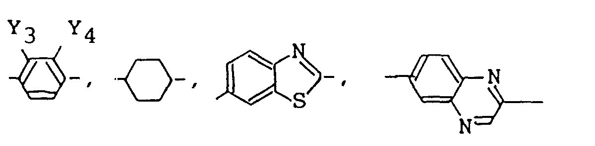
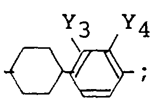
- the liquid crystal composition as the chiral smectic liquid crystal used in the liquid crystal device may preferably comprise at least two compounds each represented by the following formulas (1), (2), (3) and (4).
- A is R1 and R2 are independently a linear or branched alkyl group having 1 - 20 carbon atoms optionally having a substituent;
- X1 and X2 are independently a single bond O, COO or OOC;
- Y1, Y2, Y3 and Y4 are independently H or F; and
- n is 0 or 1.
- A is R1 and R2 are independently a linear or branched alkyl group having 1 - 20 carbon atoms optionally having a substituent; X1 and X2 are independently a single bond O, COO or OOC; and Y1, Y2, Y3 and Y4 are independently H or F.
- A: or R1 and R2 are independently a linear or branched alkyl group having 1 - 20 carbon atoms optionally having a substituent X1 and X2 are independently a single bond O, COO or OOC; and Y1, Y2, Y3 and Y4 are independently H or F.
- R1 and R2 are independently a linear or branched alkyl group having 1 - 20 carbon atoms optionally having a substituent; X1 and X2 are independently a single bond, O, COO or OOC; and Y1, Y2, Y3 and Y4 are independently H or F.
- Figure 1 shows a schematic sectional view of a liquid crystal device 80 according to an embodiment of the invention.
- the liquid crystal device 80 includes a pair of substrates 81a and 81b; electrodes 82a and 82b disposed on the substrates 81a and 81b, respectively; insulating films 83a and 83b disposed on the electrodes 82a and 82b, respectively; a surface potential adjusting film 88 disposed on the insulating film 83b, alignment control films 84a and 84b disposed on the insulating film 83a and the surface potential adjusting film 88, respectively; a chiral smectic liquid crystal 85 disposed between the alignment control films 84a and 84b; a spacer 86 disposed together with the liquid crystal 85 between the alignment control films 84a and 84b; and a pair of cross-nicol polarizers 87a and 87b (with crossed polarizing axes at right angles) sandwiching the pair of substrates 81a and 81b.
- Each of the substrates 81a and 81b comprises a transparent material, such as glass or plastics, and is coated with, e.g., a plurality of stripe electrodes 82a (82b) of In 2 O 3 or ITO (indium tin oxide) for applying a voltage to the liquid crystal 85.
- These electrodes 82b and 82b are arranged in a (dot-)matrix form.
- one of the substrates 81a and 81b is provided with a matrix electrode structure wherein dot-shaped transparent electrodes are disposed as pixel electrodes in a matrix form and each of the pixel electrodes is connected to a switching or active element, such as a TFT (thin film transistor) or MIM (metal-insulator-metal), and the other substrate may be provided with a counter (common) electrode on its entire surface or in an prescribed pattern, thus constituting an active matrix-type liquid crystal device.
- a switching or active element such as a TFT (thin film transistor) or MIM (metal-insulator-metal
- the insulating films 83a and 83b e.g., of SiO 2 , TiO 2 or Ta 2 O 5 having a function of preventing an occurrence of short circuit may be disposed, respectively, as desired.
- the surface potential adjusting film 88 (for adjusting the potential difference between the substrates 81a and 81b) is formed as an underlying layer for the alignment control film 14b.
- the surface potential adjusting film 88 may be formed on both of the pair of the insulating films 13a and 13b.
- the surface potential adjusting film 88 it is possible use as a principal component (insulating matrix material) a film having a lower dispersion term of a surface energy them a material for the alignment control film 84a (84b) of, e.g., polyamide or polyimide. Specifically, it is possible to use a film of a ladder-type polysiloxane or an organic compound-modified silica.
- the surface potential adjusting film 88 may preferably have a volume resistivity of 1.0x10 4 - 1.0x10 10 ohm.cm.
- the potential difference adjusting film 88 it is possible to use a film comprising an insulating matrix (binder) and fine particles (electroconductive fine particles dispersed therein so as to more appropriately control the above-mentioned electrical properties (volume resistivity, surface potential).
- Examples thereof may include films, preferably coating-type films, comprising a matrix of SiOx, TiOx, ZrOx, another meltable inorganic oxide, and a polymer, such as siloxane polymer, and fine particles dispersed therein of oxides, inclusive of group II element oxides, such as ZnO, CdO and ZnCdOx; and group IV element oxides, such as GeO 2 , SnO 2 , GeSnOx, TiO 2 , ZrO 2 and TiZrOx; and group IV semiconductors, such as Si and SiC so as to control the film property and the resistivity of the film.
- films preferably coating-type films, comprising a matrix of SiOx, TiOx, ZrOx, another meltable inorganic oxide, and a polymer, such as siloxane polymer, and fine particles dispersed therein of oxides, inclusive of group II element oxides, such as ZnO, CdO and ZnCdOx; and group IV element
- Examples of the electroconductivity-controlling impurities added to the fine particles may include: n-type impurities (donor: impurities enhancing electron-conductivity) comprising group III elements, such as B, Al, Ga and In, and p-type impurities (acceptors: impurities enhancing hole-conductivity) comprising group I elements, such as Cu, Ag, Au and Li, respectively, for the group II element oxides; and n-type impurities comprising group V elements, such as P, As, Sb and Bi, and p-type impurities comprising group III elements, such as B, Al, Ga and In, respectively, for the group IV element oxides or semiconductors.
- a donor is added in case where the substrate having the potential difference adjusting film has a positive surface potential, and an acceptor is added in case of a negative surface potential.
- the concentration of the impurity can vary depending on the kind of the material (the fine particles, a combination of impurities) and the crystal state (density of crystal defect) but may preferably be determined so as to provide a free electron or free hole concentration of ca. 1.0x10 11 - 1.0x10 14 atm/cm 3 .
- the impurity may be actually added in an amount of preferably 1.0x10 17 - 1.0x10 20 atm/cm 3 (ca. 0.01 - 1 % of the matrix material) while taking the addition efficiency of the impurity into consideration.
- the alignment control films 14a and 14b are disposed so as to control the alignment state of the liquid crystal 15 contacting the alignment control films 84a and 84b. At least one (preferably both) of the alignment control films 84a and 84b are subjected to a uniaxial aligning treatment (e.g., rubbing).
- a uniaxial aligning treatment e.g., rubbing
- Such an alignment control film 84a (84b) may be prepared by forming a film of an organic material (such as polyimide, polyimideamide, polyamide or polyvinyl alcohol through wet coating with a solvent, followed by drying and rubbing in a prescribed direction or by forming a deposited film of an inorganic material through an oblique vapor deposition such that an oxide (e.g., SiO) or a nitride is vapor-deposited onto a substrate in an oblique direction with a prescribed angle to the substrate.
- an organic material such as polyimide, polyimideamide, polyamide or polyvinyl alcohol
- the alignment control films 84a and 84b may appropriately be controlled to provide liquid crystal molecules of the above-mentioned liquid crystal 85 disposed therebetween with a prescribed pretilt angle ⁇ (an angle formed between the liquid crystal molecule and the alignment control film surface at the boundaries with the alignment control films) by changing the material and treating conditions (of the uniaxial aligning treatment).
- the respective uniaxial aligning treatment (rubbing) directions may appropriately be set in an anti-parallel relationship, a parallel relationship or a crossed relationship.
- the substrates 81a and 81b are disposed opposite to each other via the spacer 86 comprising e.g., silica beads for determining a distance (i.e., cell gap) therebetween, preferably in the range of 0.3 - 10 ⁇ m, in order to provide a uniform uniaxial aligning performance and such an alignment state that an average molecular axis of the liquid crystal molecules under no electric field application is substantially aligned with an average uniaxial aligning treatment axis or a bisector of two uniaxial aligning treatment: axes) although the cell gap varies its optimum range and its upper limit depending on the liquid crystal material used.
- a distance i.e., cell gap
- a liquid crystal device having the above-mentioned liquid crystal cell structure can be prepared by using a chiral smectic liquid crystal material 85 while adjusting the composition thereof, and further by appropriate adjustment of the liquid crystal material treatment, the device structure including a material, and a treatment condition for alignment control films 84a and 84b.
- the liquid crystal material may preferably be placed in an alignment state such that the liquid crystal molecules are aligned to provide an average molecular axis to be mono-stabilized in the absence of an electric field applied thereto and, under application of voltages of one polarity (a first polarity), are tilted in one direction from the average molecular axis under no electric field to provide a tilting angle which varies continuously from the average molecular axis of the monostabilized position depending on the magnitude of the applied voltage.
- a first polarity one polarity
- a maximum tilting angle ⁇ 1 obtained under application of the first polarity voltages based on the monostabilized position is substantially larger than a maximum tilting angle ⁇ 2 formed under application of the second polarity voltages, i.e., ⁇ 1 > ⁇ 2.
- ⁇ 2 may be substantially zero deg., i.e., the average molecular axis is not moved substantially under application of the second polarity voltages.
- the liquid crystal device of embodiments of the invention may be used as a color liquid crystal device by providing one of the pair of substrates 81a and 81b with a color filter comprising color filter segments (color portions) of at least red (R), green (G) and blue (B). It is also possible to effect a full-color display by successively switching (lighting) a light source comprising R light source, G light source and B light source emitting color light fluxes to effect color mixing in a time division (sequential) manner.
- the liquid crystal device of embodiments of the invention is of a light-transmission type such that the pair of substrates 81a and 81b are sandwiched between a pair of polarizers to optically modulate incident light (e.g., issued from an external light source) through one of the substrates to be passed through the other substrate.
- the liquid crystal device of embodiments of the invention may be modified into a reflection-type liquid crystal device by providing a reflection plate to either one of the substrates 81a and 81b or using a combination of one of the substrates per se formed of a reflective material or with a reflecting member thereon and the other substrate provided with a polarizer outside thereof, thus optically modulating incident light and reflected light and causing the reflected light to pass through the substrate on the light incident side.
- liquid crystal display apparatus capable of effecting a gradational display based on the above-mentioned alignment characteristic such that under voltage application, a resultant tilting angle varies continuously from the monostabilized position of the average molecular axis (of liquid crystal molecules) and a corresponding emitting light quantity continuously changes, depending on the applied voltage.
- an active matrix substrate provided with a plurality of switching elements (e.g., TFT (thin film transistor) or MIM (metal-insulator-metal)) in combination with a drive circuit (drive means), thus effecting an active matrix drive based on amplitude modulation to allow a gradational display in an analog gradation manner.
- switching elements e.g., TFT (thin film transistor) or MIM (metal-insulator-metal)
- Figure 2 shows a schematic plan view of such a display apparatus including a liquid crystal device and a drive circuit (means) and principally illustrates a structure on the active matrix substrate side.
- a liquid crystal device (panel) 90 includes a structure such that scanning signal lines (gate lines) (G1, G2, G3, G4, G5, ...) connected to a scanning signal driver 91 (drive means) and data signal lines (source lines) (S1, S2, S3, S4, S5, ...) connected to a data signal driver 92 (drive means) are disposed to intersect each other at right angles in an electrically isolated state, thus forming a plurality of pixels (5x5 in Figure 2) each at intersection thereof.
- Each pixel is provided with a thin film transistor (TFT) 94 as a switching element and a pixel electrode 95.
- TFT thin film transistor
- the scanning signal (gate) lines (G1, G2, ...) are connected with gate electrodes (not shown) of the TFT 94, respectively, and the data signal (source) lines (S1, S2, ...) are connected with source electrodes (not shown) of the TFT 94, respectively.
- the pixel electrodes 95 are connected with drain electrodes (not shown) of the TFT 94, respectively.
- a gate voltage is supplied to the gate lines (G1, G2, ...) from the scanning signal driver 91 by effecting scanning selection in, e.g., a line-sequential manner.
- the source lines (S1, S2, ...) are supplied with a data signal voltage depending on writing data for each pixel from the data signal driver 92.
- the thus-supplied gate and data signal voltages are applied to each pixel electrode 95 via the TFT 94.
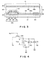
- Figure 3 shows a sectional structure of each pixel portion (corr. to 1 bit) in the panel structure shown in Figure 2.
- a layer of a chiral smectic liquid crystal layer 49 is sandwiched between an active matrix substrate or plate 20 provided with a TFT 94 and a pixel electrode 95 and an opposing substrate or plate 40 provided with a common electrode 42, thus providing a liquid crystal capacitor (Clc) 31 of the liquid crystal layer 49.
- the active matrix substrate 20 includes an amorphous silicon (a-Si) TFT as the TFT 94.
- the TFT may be of a polycrystalline-Si (p-Si) type.
- the TFT 94 is formed on a substrate 21 of, e.g., glass and includes: a gate electrode 22 connected with the gate lines (G1, G2, ... shown in Figure 2); an insulating film (gate insulating film) 23 of, e.g., silicon nitride (SiNx) formed on the gate electrode 22; an a-Si layer 24 formed on the insulating film 23; n + a-Si layers 25 and 26 formed on the a-Si layer 24 and spaced apart from each other; a source electrode 27 formed on the n + a-Si layer 25; a drain electrode 28 formed on the n + a-Si layer 26 and spaced apart from the source electrode 27; a channel protective film 29 partially covering the a-Si layer 24 and the source and drain electrodes 27 and 28.
- gate insulating film 23 of, e.g., silicon nitride (SiNx) formed on the gate electrode 22
- an a-Si layer 24 formed on the
- the source electrode 27 is connected with the source lines (S1, S2, ... shown in Figure 2) and the drain electrode 28 is connected with the pixel electrode 95 ( Figure 2) of a transparent conductor film (e.g., ITO film).
- the TFT 94 is placed in an "ON" state by applying a gate pulse to the gate electrode 22 during a scanning selection period of the corresponding gate line.
- a structure constituting a holding or storage capacitor (Cs) 32 is formed by the pixel electrode 95, a storage capacitor electrode 30 disposed on the substrate 21, and a portion of the insulating film 23 sandwiched therebetween.
- the structure (storage capacitor) (Cs) 32 is disposed in parallel with the liquid crystal capacitor 31.
- the storage capacitor electrode 30 is formed of a transparent conductor film (e.g., ITO film).
- an alignment film 43a provided with a uniaxial alignment axis by, e.g., rubbing for controlling an alignment state of the liquid crystal 49 is formed.
- the opposing substrate 40 includes a substrate (e.g., glass substrate) 41; a common electrode 42 having a uniform thickness disposed on the entire substrate 41; and an alignment film 43b having a uniform thickness, disposed on the common electrode 42, for controlling an alignment state of the liquid crystal 49.
- a substrate e.g., glass substrate
- a common electrode 42 having a uniform thickness disposed on the entire substrate 41
- an alignment film 43b having a uniform thickness, disposed on the common electrode 42, for controlling an alignment state of the liquid crystal 49.
- the above liquid crystal device shown in Figure 3 is sandwiched between a pair of cross-nicol polarizers (not shown) (provided with polarizing axes disposed perpendicular to each other) to constitute a light-transmission type liquid crystal device.
- Figure 4 shows an example of an equivalent circuit for each pixel portion of such a liquid crystal device shown in Figure 3.
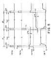
- one frame period for displaying a prescribed data is divided into a plurality of field periods (e.g., 1F and 2F in Figure 5) each for a prescribed image.
- each of the field periods 1F and 2F a prescribed transmitted light quantity depending on a prescribed image data for each field period is obtained. Further, in each frame period, an average of the transmitted light quantities in the field periods 1F and 2F is obtained to provide a prescribed image.
- Figure 5 shows at (a) a voltage waveform applied to one gate line (e.g., G1 shown in Figure 2) (as a scanning signal line) connected with each pixel.
- G1 gate line
- Figure 2 shows at (a) a voltage waveform applied to one gate line (e.g., G1 shown in Figure 2) (as a scanning signal line) connected with each pixel.
- the gate lines G1, G2, ... shown in Figure 2 are selected in a line-sequential manner in each of the field periods 1F and 2F.
- each gate electrode 22 connected with a corresponding gate line is supplied with a prescribed gate voltage Vg in a selection period T on of each field period (e.g., 1F), thus placing the TFT 94 in an "ON" state.
- a non-selection period T off (of, e.g., the field period 1F) corresponding to a period in which other gate lines are selected, the gate electrode 22 is not supplied with the gate voltage Vg, thus placing the TFT 94 in an "OFF" state (high-resistance state).
- a prescribed and same gate line is selected and a corresponding gate electrode 22 is supplied with the gate voltage Vg.
- Figure 5 shows at (b) a voltage waveform applied to one source line (e.g., S1 shown in Figure 2) (as a data signal line) connected to the pixel concerned.
- S1 source line
- a prescribed source voltage (data signal voltage) Vs having a prescribed potential providing a writing data (pulse) to the pixel concerned is applied to a source electrode 27 through the source line connected with the pixel based on a potential Vc of a common electrode 42 as a reference potential.
- a positive-polarity source voltage Vs having a potential Vx (based on a reference potential Vc) providing a desired optical state or display data (transmittance) based on a voltage-transmittance (V-T) characteristic for the liquid crystal used is applied to the source electrode 27 concerned.
- the TFT 94 is in an "ON" state, whereby the positive-polarity source voltage Vx applied to the source electrode 27 is supplied to a pixel electrode 95 via a drain electrode 28, thus charging a liquid crystal capacitor (Clc) 31 and a storage capacitor (Cs) 32.
- the potential of the pixel electrode 95 becomes a level equal to that of the positive-polarity source (data signal) voltage Vx.
- the TFT 94 is in an "OFF" (high-resistance) state.
- T off of 1F in the liquid crystal cell, the liquid crystal capacitor (Clc) 31 and the storage capacitor (Cs) 32 retain the electric charges therein, respectively, charged in the selection period T on to keep the (positive-polarity) voltage Vx.
- the liquid crystal layer 49 of the pixel concerned is supplied with the voltage Vx through the first field period 1F to provide thereat a desired optical state (transmitted light quantity) depending on the voltage Vx.
- the TFT 84 is in an "ON" state, whereby the negative-polarity source voltage -Vx is supplied to a pixel electrode 95, thus charging a liquid crystal capacitor (Clc) 31 and a storage capacitor (Cs) 32.
- the potential of the pixel electrode 95 becomes a level equal to that of the negative-polarity source (data signal) voltage -Vx.
- the TFT 94 is in an "OFF" (high-resistance) state.
- the liquid crystal capacitor (Clc) 31 and the holding capacitor (Cs) 32 retain the electric charges therein, respectively, charged in the selection period Ton to keep the (negative-polarity) voltage -Vx.
- the liquid crystal layer 49 of the pixel concerned is supplied with the voltage -Vx through the second field period 2F to provide thereat a desired optical state (transmitted light quantity) depending on the voltage -Vx.
- Figure 5 shows at (d) an example of an actual optical response at the pixel concerned.
- an applied voltage through two field periods 1F and 2F comprises the positive-polarity voltage Vx' in the first field period 1F and the negative-polarity voltage -Vx' (having the same amplitude (absolute value) as Vx') in the second field period 2F.
- a higher luminance or transmitted light quantity Tx is obtained in the first field period 1F but in the second field period 2F, a lower luminance or transmitted liquid quantity Ty which is closer to zero but a non-zero value because the relationship of ⁇ 1 > ⁇ 2 is satisfied.
- a gradational display of a prescribed level at each pixel is continuously performed by dividing one frame period into a first field pixel 1F providing a higher transmitted light quantity and a second field period 2F providing a lower transmitted light quantity, thus resulting in a timewise aperture rate of at most 50 % to improve a human-sensible high-speed responsiveness with respect to motion picture display.
- the resultant transmitted light quantity is not completely zero due to a slight switching (inversion) performance of liquid crystal molecules, thus ensuring a certain human-sensible luminance through the entire frame period.
- the polarity of the voltage (Vx or -Vx) is changed alternately for every field period (1F or 2F) (i.e., polarity-inversion for each field period), whereby the voltage actually applied to the liquid crystal layer 49 is continuously changed in an alternating manner to suppress a deterioration of the liquid crystal material used even in a continuous display operation for a long period.
- a resultant transmitted light quantity corresponds to an average of Tx and Ty. Accordingly, in order to obtain a further higher transmitted light quantity in each frame period, it is preferred to apply a source (data signal) voltage Vs providing a transmitted light quantity higher than Tx in the first field period 1F by a prescribed level.
- the liquid crystal device of embodiments of the invention may be applicable to a full-color liquid crystal display apparatus using the liquid crystal device in combination with a plurality of color light sources of at least red (R), green (G) and blue (B) without using a color filter, as desired, thus effecting color mixing in a time-division multiplexing manner.
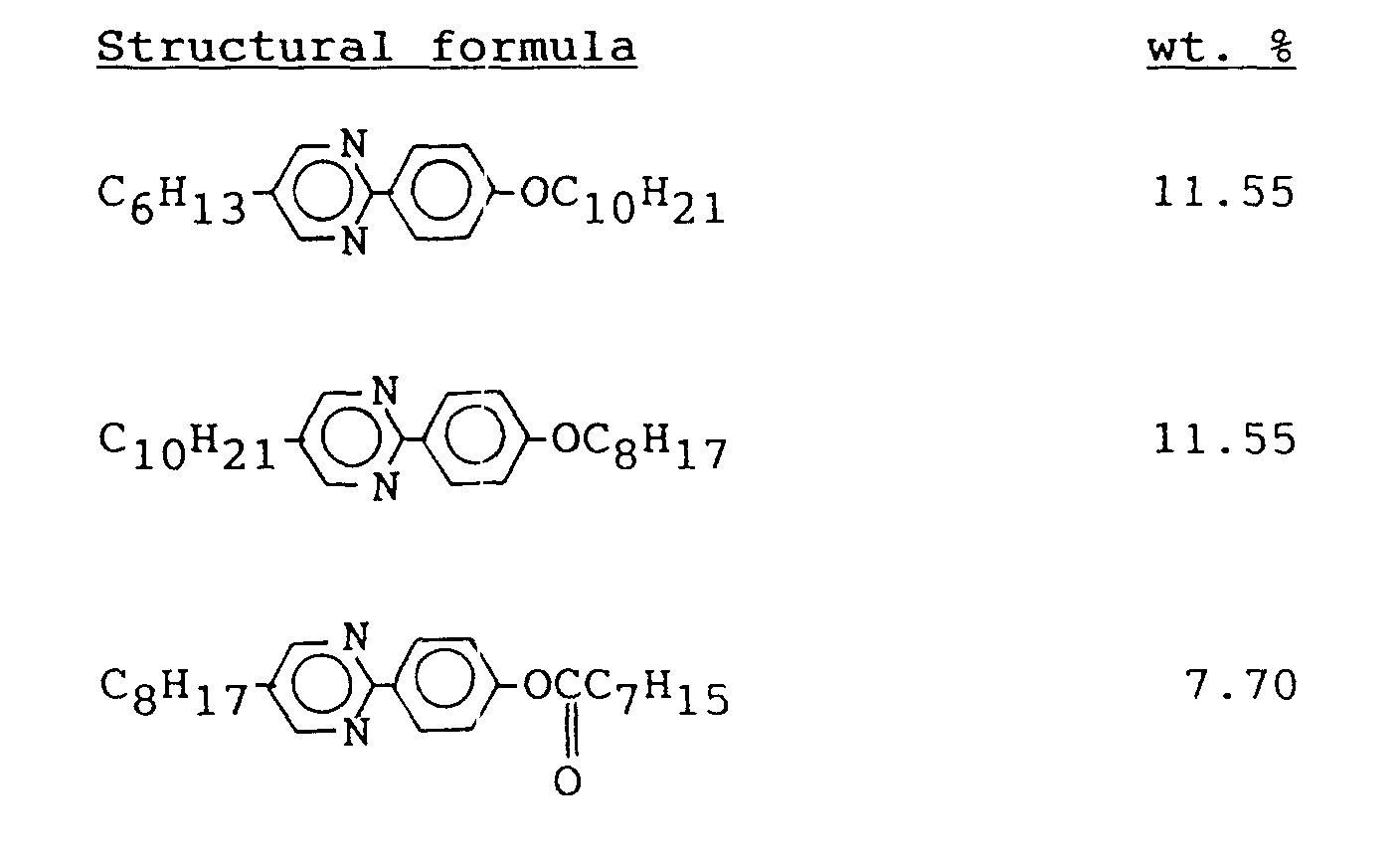
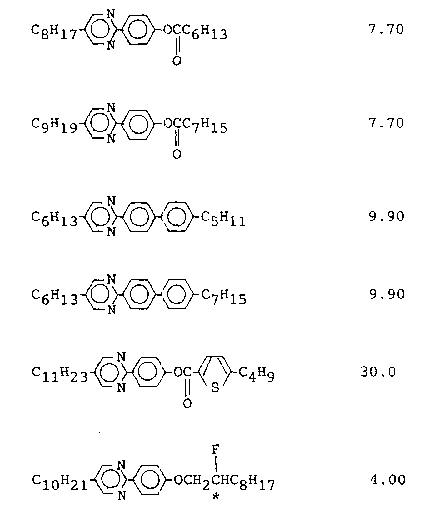
- a chiral smectic liquid crystal composition LC-1 was prepared by mixing the following compounds in the indicated proportions.
- the thus-prepared liquid crystal composition LC-1 showed the following phase transition series and physical properties.
- the values of spontaneous polarization Ps, tilt angle H ⁇ , and layer inclination angle 6 in smectic layer referred to herein are based on values measured according to the following methods.
- the spontaneous polarization Ps was measured according to "Direct Method with Triangular Waves for Measuring Spontaneous Polarization in Ferroelectric Liquid Crystal", as described by K. Miyasato et al (Japanese J. Appl. Phys. 22, No. 10, pp. L661-(1983)).
- a liquid crystal device was sandwiched between right angle-cross nicol polarizers and rotated horizontally relative to the polarizers under application of an AC voltage of ⁇ 12.5 V to ⁇ 50 V and 1 to 100 Hz between the upper and lower substrates of the device while measuring a transmittance through the device by a photomultiplier (available from Hamamatsu Photonics K.K.) to find a first extinct position (a position providing the lowest transmittance) and a second extinct position.
- a tilt angle H was measured as half of the angle between the first and second extinct positions.
- the method used was basically similar to the method used by Clark and Largerwal (Japanese Display '86, Sept. 30 - Oct. 2, 1986, p.p. 456 - 458) or the method of Ohuchi et al (J.J.A.P., 27 (5) (1988), p.p. 725 - 728).
- the measurement was performed by using a rotary cathode-type X-ray diffraction apparatus (available from MAC Science), and 80 ⁇ m-thick microsheets (available from Corning Glass Works) were used as the substrates so as to minimize the X-ray absorption with the glass substrates of the liquid crystal cells.
- a blank cell was prepared in the following manner.
- a pair of 1.1 mm-thick glass substrates each provided with a 700 ⁇ -thick transparent electrode of ITO film was provided except that one of the pair of glass substrate was formed in an active matrix substrate provided with a plurality of a-Si TFTs and a silicone nitride (gate insulating) film and the other glass substrate (counter substrate) was provided with a color filter including color filter segments of red (R), green (G) and blue (B).
- the thus prepared blank cell (active matrix cell) having a structure had a picture area size of 10.4 inches including a multiplicity of pixels (800x600xRGB).
- nylon 66 available from Toray K.K.
- formic acid was spin-coated, followed by hot-dryig at 180 °C for 1 hour, to form a nylon film having a thickness of 500 ⁇ .
- Each of the thus-obtained nylon films was subjected to rubbing treatment (as a uniaxial aligning treatment) with a nylon cloth under the following conditions to provide an alignment control film.
- Rubbing roller a 85 mm-dia. roller about which a nylon cloth ("NF-77", mfd. by Teijin K.K.) was wound.
- the thus-treated pair of substrates were applied to each other with a sealing agent (epoxy resin) so that the rubbing treating axes were in parallel with each other but oppositely directed (anti-parallel relationship), followed by baking for curing to prepare a blank cell with a uniform cell gap.
- the liquid crystal composition LC-1 was injected into the above-prepared blank cell in its cholesteric phase state and gradually cooled to a temperature providing chiral smectic C phase to prepare a liquid crystal device (panel) A.
- a liquid crystal device B was prepared in the same manner as in Example 1 except that the thickness of the nylon film (50 ⁇ ) for the counter substrate was changed to 100 ⁇ .
- a liquid crystal device C was prepared in the same manner as in Example 1 except that the SnOx-based film (2000 ⁇ ) and of the nylon film (50 ⁇ ) for the counter substrate was changed to a 500 ⁇ -thick nylon film (which was prepared in the same manner as in the case of the active matrix substrate).
- a liquid crystal device D was prepared in the same manner as in Example 1 except that the SnOx-based film (2000 ⁇ ) and of the nylon film (50 ⁇ ) for the counter substrate was changed to a 100 ⁇ -thick nylon film (which was prepared in the same manner as in the case of the active matrix substrate).
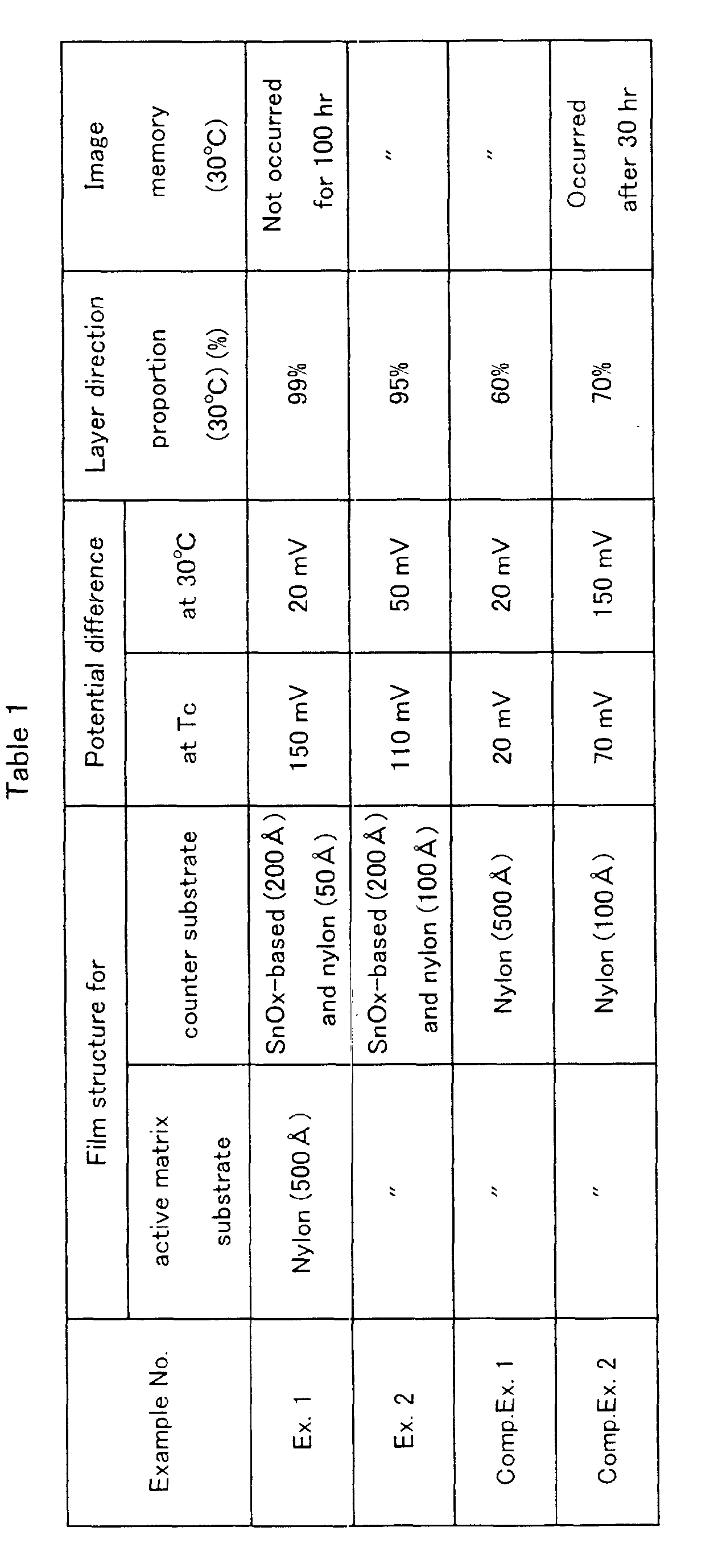
- each of the liquid crystal devices A, B, C and D were evaluated as to a proportion of layer (formation) direction at 30 °C and image memory in the following manner.
- the liquid crystal device was sandwiched between a pair of cross-nicol polarizers so that the polarizing axis was aligned with a layer direction (of liquid crystal molecules) providing the darkest (black) state. If there was a region in which liquid crystal molecules were directed in another layer direction, escape of light was caused to occur in the region, thus providing a white state.
- the layer direction was evaluated as a proportion (%) (areal ratio) of the black state region per the entire region.
- Two electrode areas were disposed adjacent to and connected to a test cell, and one electrode area was energized and the other electrode was not energized (left standing). After a prescribed time, the two electrodes areas were supplied with a voltage (for providing a halftone state). At that time, when a difference in luminance between the two electrodes areas was confirmed by eye observation, the test cell was evaluated such that the image memory occurred in the cell.
- liquid crystal devise A and B providing a potential difference of at least 100 mV at Tc showed a very high proportion of layer direction (99 % and 95 %) and an excellent image memory-prevention performance.
- the liquid crystal device C (potential difference of 20 mV) showed an excellent image memory-prevention performance due to its symmetrical film structure, the liquid crystal device C showed a smaller proportion of layer direction (60 %) leading to a poor colorant.
- the liquid crystal device D (potential difference of 70 mV) showed a smaller proportion of layer direction (70 %) and a poor image-memory prevention performance.
- the liquid crystal device even if a liquid crystal device is once placed in a cholesteric (or isotropic) phase state during a storage thereof, the liquid crystal device is caused to have a uniform smectic layer (formation) direction due to a sufficient potential difference (at least 100 mV) when returned to chiral smectic phase state.
- the liquid crystal device of embodiments of the invention is free from its upper-limit storage temperature.
- the liquid crystal device shows a smaller potential difference (at most 100 mV) at an operation temperature (e.g., at 30 °C), thus preventing continuous application of a DC voltage component leading to the image memory phenomenon.
- the liquid crystal device is combined with a drive means to provide a liquid crystal apparatus excellent in driving and display performances.
Landscapes
- Physics & Mathematics (AREA)
- Chemical & Material Sciences (AREA)
- Crystallography & Structural Chemistry (AREA)
- Nonlinear Science (AREA)
- General Physics & Mathematics (AREA)
- Engineering & Computer Science (AREA)
- Optics & Photonics (AREA)
- Liquid Crystal (AREA)
- Computer Hardware Design (AREA)
- Theoretical Computer Science (AREA)
- Mathematical Physics (AREA)
- Liquid Crystal Substances (AREA)
Abstract
Description




Claims (12)
- A chiral smectic liquid crystal device, comprising:a chiral smectic liquid crystal exhibiting a phase transition series on temperature decrease of isotropic liquid phase (Iso), cholesteric phase (Ch) and chiral smectic C phase (SmC*) or of isotropic phase (Iso) and chiral smectic C phase (SmC*), anda pair of substrates each provided with an electrode for applying a voltage to the liquid crystal and a uniaxial alignment axis for aligning the liquid crystal, at least one of the substrates being provided with a polarizer and the pair of substrates being oppositely disposed to sandwich the liquid crystal so as to form a plurality of pixels each provided with an active element connected to an associated electrode on at least one of the substrates, whereinthe liquid crystal device further includes means for providing a difference in potential between the pair of substrates of at least 100 mV under a condition free from application of an external electric field in a temperature range of Tc ±2 °C where Tc denotes a phase transition temperature from Ch to SmC* or from Iso to SmC*.
- A device according to Claim 1 or any of Claims 8 to 12, wherein said means provides a difference in potential between the substrates of at most 100 mV at least in a temperature range of 10 - 50 °C under a condition free from application of an external electric field.
- A device according to Claim 1 or any of Claims 8 to 12, wherein said difference in potential in the temperature range of Tc ±2 °C is 150 mV to 3 V.
- A device according to Claim 3, wherein said means provides a difference in potential between the substrates of at most 100 mV at least in a temperature range of 10 - 50 °C under a condition free from application of an external electric field.
- A device according to Claim 1 or any of Claims 8 to 12, wherein said means comprises a film formed of at least one material providing a difference in potential between the substrates of at least 150 mV at least in a temperature range of 10 - 75 °C when provided to at least one of opposing surfaces of the pair of substrates.
- A device according to Claim 5, wherein said temperature range is 10 - 50 °C.
- A liquid crystal apparatus, comprising: a liquid crystal device according to any one of Claims 1 to 6 or 8 to 12 and drive means for driving the liquid crystal device.
- A chiral smectic liquid crystal device, comprising:a chiral smectic liquid crystal exhibiting a phase transition series on temperature decrease of isotropic liquid phase (Iso), cholesteric phase (Ch) and chiral smectic C phase (SmC*) or of isotropic phase (Iso) and chiral smectic C phase (SmC*), andfirst and second substrates each provided with an electrode for applying a voltage to the liquid crystal, at least one of the substrates being provided with a uniaxial alignment film for aligning the liquid crystal and said first and second substrates being oppositely disposed to sandwich the liquid crystal, whereinthe liquid crystal device further includes means for providing a difference in potential between said first and second substrates of at least 100 mV under a condition free from application of an external electric field in a temperature range of Tc ±2 °C where Tc denotes a phase transition temperature from Ch to SmC* or from Iso to SmC*.
- A device according to Claim 8, wherein each of said first and second substrates is provided with a uniaxial alignment film for aligning the liquid crystal.
- A device according to Claims 8 or 9 arranged to form a plurality of pixels.
- A device according to Claim 10, wherein the electrode on said first substrate is arranged as a plurality of pixel electrodes, each pixel electrode being provided with an active element.
- A device according to any one of Claims 8 to 11, further comprising at least one polarizer.
Applications Claiming Priority (2)
| Application Number | Priority Date | Filing Date | Title |
|---|---|---|---|
| JP2000106383 | 2000-04-07 | ||
| JP2000106383A JP3466986B2 (en) | 2000-04-07 | 2000-04-07 | Chiral smectic liquid crystal element and liquid crystal device |
Publications (2)
| Publication Number | Publication Date |
|---|---|
| EP1143289A2 true EP1143289A2 (en) | 2001-10-10 |
| EP1143289A3 EP1143289A3 (en) | 2007-03-07 |
Family
ID=18619558
Family Applications (1)
| Application Number | Title | Priority Date | Filing Date |
|---|---|---|---|
| EP01303289A Withdrawn EP1143289A3 (en) | 2000-04-07 | 2001-04-06 | Chiral smectic liquid crystal device |
Country Status (4)
| Country | Link |
|---|---|
| US (1) | US6710842B2 (en) |
| EP (1) | EP1143289A3 (en) |
| JP (1) | JP3466986B2 (en) |
| KR (1) | KR20010090771A (en) |
Families Citing this family (14)
| Publication number | Priority date | Publication date | Assignee | Title |
|---|---|---|---|---|
| KR100512622B1 (en) * | 2000-06-08 | 2005-09-02 | 마쯔시다덴기산교 가부시키가이샤 | Image display and method for displaying image |
| JP4197233B2 (en) * | 2002-03-20 | 2008-12-17 | 株式会社日立製作所 | Display device |
| JP4605978B2 (en) * | 2002-08-30 | 2011-01-05 | 富士通株式会社 | Manufacturing method of liquid crystal display device |
| KR100872713B1 (en) * | 2002-08-30 | 2008-12-05 | 엘지디스플레이 주식회사 | Electric field alignment method of ferroelectric liquid crystal display device and driving method and device of ferroelectric liquid crystal display device using same |
| JP3796499B2 (en) * | 2002-11-06 | 2006-07-12 | キヤノン株式会社 | Color display element, color display element driving method, and color display device |
| JP4566526B2 (en) * | 2003-07-09 | 2010-10-20 | キヤノン株式会社 | Liquid crystal display |
| JP4208763B2 (en) * | 2004-04-28 | 2009-01-14 | キヤノン株式会社 | Color display element and color liquid crystal display element |
| JP4332515B2 (en) * | 2004-04-28 | 2009-09-16 | キヤノン株式会社 | Liquid crystal display |
| JP2005321458A (en) * | 2004-05-06 | 2005-11-17 | Canon Inc | Color liquid crystal display element |
| WO2006123803A1 (en) * | 2005-05-19 | 2006-11-23 | Canon Kabushiki Kaisha | Liquid crystal display device |
| WO2008072528A1 (en) * | 2006-12-08 | 2008-06-19 | Canon Kabushiki Kaisha | Liquid crystal optical device manufacturing process |
| US8298516B2 (en) * | 2006-12-22 | 2012-10-30 | Douglas Anderson | Calculus dissolving dental composition and methods for using same |
| JP6258569B2 (en) * | 2008-08-04 | 2018-01-10 | ザ、トラスティーズ オブ プリンストン ユニバーシティ | Hybrid dielectric materials for thin film transistors |
| US10434948B2 (en) * | 2016-06-03 | 2019-10-08 | Gentex Corporation | Display system with phase oriented reflective control |
Family Cites Families (26)
| Publication number | Priority date | Publication date | Assignee | Title |
|---|---|---|---|---|
| JP2550054B2 (en) | 1987-03-17 | 1996-10-30 | 旭硝子株式会社 | Ferroelectric smectic liquid crystal electro-optical device |
| JP2872372B2 (en) | 1990-09-04 | 1999-03-17 | キヤノン株式会社 | Liquid crystal compound, liquid crystal composition containing the same, and liquid crystal device using the same |
| JP3095927B2 (en) | 1993-02-10 | 2000-10-10 | キヤノン株式会社 | Optically active compound, liquid crystal composition containing the same, method of using the same, liquid crystal element and display device using the same |
| DE69526291D1 (en) * | 1994-08-04 | 2002-05-16 | Canon Kk | liquid crystal device |
| JP3136052B2 (en) * | 1994-09-30 | 2001-02-19 | シャープ株式会社 | Ferroelectric liquid crystal device |
| JP3119340B2 (en) | 1995-01-31 | 2000-12-18 | キヤノン株式会社 | Liquid crystal composition, liquid crystal element having the same, and liquid crystal device having the same |
| JP3119342B2 (en) * | 1995-01-31 | 2000-12-18 | キヤノン株式会社 | Liquid crystal composition, liquid crystal element having the same, and liquid crystal device having the same |
| JP3043257B2 (en) | 1995-01-31 | 2000-05-22 | キヤノン株式会社 | Liquid crystal composition, liquid crystal element having the same, and liquid crystal device having the same |
| JP3119341B2 (en) | 1995-01-31 | 2000-12-18 | キヤノン株式会社 | Liquid crystal composition, liquid crystal element having the same, and liquid crystal device having the same |
| JPH07306421A (en) * | 1995-04-20 | 1995-11-21 | Canon Inc | Ferroelectric liquid crystal element |
| DE69618413T2 (en) | 1995-10-12 | 2002-06-20 | Canon K.K., Tokio/Tokyo | Liquid crystal composition, liquid crystal device and liquid crystal display apparatus |
| US5932136A (en) | 1995-10-20 | 1999-08-03 | Canon Kabushiki Kaisha | Liquid crystal device and liquid crystal apparatus |
| JPH09146126A (en) | 1995-11-22 | 1997-06-06 | Canon Inc | Liquid crystal device and information transmission device |
| JPH08211393A (en) * | 1995-12-07 | 1996-08-20 | Nippondenso Co Ltd | Method for manufacturing liquid crystal electro-optical element |
| US5885482A (en) | 1995-12-28 | 1999-03-23 | Canon Kabushiki Kaisha | Liquid crystal device, production process thereof and liquid crystal apparatus |
| JP3093627B2 (en) | 1996-02-09 | 2000-10-03 | キヤノン株式会社 | Manufacturing method of liquid crystal display device |
| JPH1090697A (en) * | 1996-09-13 | 1998-04-10 | Sony Corp | Manufacturing method of liquid crystal element |
| JPH1114991A (en) * | 1997-06-20 | 1999-01-22 | Canon Inc | Liquid crystal element |
| JPH11100577A (en) | 1997-07-31 | 1999-04-13 | Canon Inc | Liquid crystal alignment method, liquid crystal element manufacturing method, liquid crystal element obtained by the manufacturing method, liquid crystal device |
| US6195147B1 (en) * | 1997-08-01 | 2001-02-27 | Canon Kabushiki Kaisha | Liquid crystal substrate with optical modulation region having different alignment control forces |
| JP3847927B2 (en) * | 1997-11-18 | 2006-11-22 | キヤノン株式会社 | Arc tube and light source device using the same |
| US6221444B1 (en) | 1998-06-10 | 2001-04-24 | Canon Kabushiki Kaisha | Liquid crystal device |
| JP2000010076A (en) | 1998-06-24 | 2000-01-14 | Canon Inc | Liquid crystal element |
| JP3535769B2 (en) | 1998-06-24 | 2004-06-07 | キヤノン株式会社 | Liquid crystal display device and method of driving the liquid crystal display device |
| JP2000275683A (en) * | 1999-03-25 | 2000-10-06 | Canon Inc | Liquid crystal element and method for driving the liquid crystal element |
| US6128064A (en) | 1999-07-14 | 2000-10-03 | Canon Kabushiki Kaisha | Liquid crystal device and liquid crystal display apparatus |
-
2000
- 2000-04-07 JP JP2000106383A patent/JP3466986B2/en not_active Expired - Fee Related
-
2001
- 2001-04-04 US US09/824,822 patent/US6710842B2/en not_active Expired - Fee Related
- 2001-04-06 EP EP01303289A patent/EP1143289A3/en not_active Withdrawn
- 2001-04-07 KR KR1020010018502A patent/KR20010090771A/en not_active Ceased
Also Published As
| Publication number | Publication date |
|---|---|
| JP3466986B2 (en) | 2003-11-17 |
| KR20010090771A (en) | 2001-10-19 |
| JP2001290177A (en) | 2001-10-19 |
| EP1143289A3 (en) | 2007-03-07 |
| US6710842B2 (en) | 2004-03-23 |
| US20020015130A1 (en) | 2002-02-07 |
Similar Documents
| Publication | Publication Date | Title |
|---|---|---|
| US7427974B2 (en) | Display apparatus, liquid crystal display apparatus and driving method for display apparatus | |
| EP0548548B1 (en) | Liquid crystal composition, liquid crystal device and display apparatus | |
| US6710842B2 (en) | Chiral smectic liquid crystal device | |
| US6417828B1 (en) | Liquid crystal composition, liquid crystal device, driving method thereof and liquid crystal apparatus | |
| US6888610B2 (en) | Liquid crystal display device having spontaneous polarization | |
| US6636193B1 (en) | Liquid crystal device | |
| US6577289B1 (en) | Liquid crystal device and display apparatus including the device | |
| US6757045B1 (en) | Liquid crystal device and liquid crystal apparatus including same | |
| US6320635B1 (en) | Liquid crystal element and manufacture thereof | |
| US20020080102A1 (en) | Process for producing liquid crystal device and driving method of the device | |
| EP1079265A2 (en) | Liquid crystal device | |
| US20020050966A1 (en) | Process for producing liquid crystal device and driving method of the device | |
| US20020054007A1 (en) | Process for producing liquid crystal device and driving method of the device | |
| US5956010A (en) | Liquid crystal apparatus and driving method | |
| US20020041353A1 (en) | Chiral smectic liquid crystal device | |
| US20020018171A1 (en) | Liquid crystal device | |
| US6420000B1 (en) | Liquid crystal device and driving method for the device | |
| US20020080101A1 (en) | Process for producing liquid crystal device and driving method of the device | |
| JPH0255328A (en) | liquid crystal display device | |
| JP2003195359A (en) | Manufacturing method of liquid crystal element | |
| US20010023739A1 (en) | Process for producing liquid crystal device | |
| JP3530799B2 (en) | Manufacturing method and driving method of chiral smectic liquid crystal device | |
| JP3219709B2 (en) | Liquid crystal element, liquid crystal device, and method of driving liquid crystal element | |
| JP2002116467A (en) | Method for manufacturing liquid crystal device and method for driving liquid crystal device | |
| JP2003140195A (en) | Liquid crystal element |
Legal Events
| Date | Code | Title | Description |
|---|---|---|---|
| PUAI | Public reference made under article 153(3) epc to a published international application that has entered the european phase |
Free format text: ORIGINAL CODE: 0009012 |
|
| AK | Designated contracting states |
Kind code of ref document: A2 Designated state(s): AT BE CH CY DE DK ES FI FR GB GR IE IT LI LU MC NL PT SE TR |
|
| AX | Request for extension of the european patent |
Free format text: AL;LT;LV;MK;RO;SI |
|
| PUAL | Search report despatched |
Free format text: ORIGINAL CODE: 0009013 |
|
| AK | Designated contracting states |
Kind code of ref document: A3 Designated state(s): AT BE CH CY DE DK ES FI FR GB GR IE IT LI LU MC NL PT SE TR |
|
| AX | Request for extension of the european patent |
Extension state: AL LT LV MK RO SI |
|
| 17P | Request for examination filed |
Effective date: 20070907 |
|
| AKX | Designation fees paid |
Designated state(s): DE FR GB IT NL |
|
| 17Q | First examination report despatched |
Effective date: 20080122 |
|
| STAA | Information on the status of an ep patent application or granted ep patent |
Free format text: STATUS: THE APPLICATION HAS BEEN WITHDRAWN |
|
| 18W | Application withdrawn |
Effective date: 20100512 |