EP1139490A1 - Surface-mount antenna and communication device with surface-mount antenna - Google Patents
Surface-mount antenna and communication device with surface-mount antenna Download PDFInfo
- Publication number
- EP1139490A1 EP1139490A1 EP00957060A EP00957060A EP1139490A1 EP 1139490 A1 EP1139490 A1 EP 1139490A1 EP 00957060 A EP00957060 A EP 00957060A EP 00957060 A EP00957060 A EP 00957060A EP 1139490 A1 EP1139490 A1 EP 1139490A1
- Authority
- EP
- European Patent Office
- Prior art keywords
- radiation electrode
- side radiation
- supplied side
- dielectric substrate
- power
- Prior art date
- Legal status (The legal status is an assumption and is not a legal conclusion. Google has not performed a legal analysis and makes no representation as to the accuracy of the status listed.)
- Granted
Links
- 230000005855 radiation Effects 0.000 claims abstract description 324
- 239000000758 substrate Substances 0.000 claims abstract description 111
- 238000010168 coupling process Methods 0.000 claims abstract description 46
- 238000005859 coupling reaction Methods 0.000 claims abstract description 46
- 230000008878 coupling Effects 0.000 claims abstract description 27
- 239000000463 material Substances 0.000 claims abstract description 24
- 238000010276 construction Methods 0.000 description 17
- 230000000694 effects Effects 0.000 description 8
- 239000000919 ceramic Substances 0.000 description 5
- 230000005684 electric field Effects 0.000 description 5
- 230000003313 weakening effect Effects 0.000 description 4
- 238000005549 size reduction Methods 0.000 description 2
- 239000000853 adhesive Substances 0.000 description 1
- 230000001070 adhesive effect Effects 0.000 description 1
- 230000005540 biological transmission Effects 0.000 description 1
- 238000010586 diagram Methods 0.000 description 1
- 230000002401 inhibitory effect Effects 0.000 description 1
- 238000010030 laminating Methods 0.000 description 1
- 239000011347 resin Substances 0.000 description 1
- 229920005989 resin Polymers 0.000 description 1
- 238000005728 strengthening Methods 0.000 description 1
Images




Classifications
-
- H—ELECTRICITY
- H01—ELECTRIC ELEMENTS
- H01Q—ANTENNAS, i.e. RADIO AERIALS
- H01Q1/00—Details of, or arrangements associated with, antennas
- H01Q1/12—Supports; Mounting means
- H01Q1/22—Supports; Mounting means by structural association with other equipment or articles
- H01Q1/2283—Supports; Mounting means by structural association with other equipment or articles mounted in or on the surface of a semiconductor substrate as a chip-type antenna or integrated with other components into an IC package
-
- H—ELECTRICITY
- H01—ELECTRIC ELEMENTS
- H01Q—ANTENNAS, i.e. RADIO AERIALS
- H01Q1/00—Details of, or arrangements associated with, antennas
- H01Q1/12—Supports; Mounting means
- H01Q1/22—Supports; Mounting means by structural association with other equipment or articles
- H01Q1/24—Supports; Mounting means by structural association with other equipment or articles with receiving set
- H01Q1/241—Supports; Mounting means by structural association with other equipment or articles with receiving set used in mobile communications, e.g. GSM
- H01Q1/242—Supports; Mounting means by structural association with other equipment or articles with receiving set used in mobile communications, e.g. GSM specially adapted for hand-held use
- H01Q1/243—Supports; Mounting means by structural association with other equipment or articles with receiving set used in mobile communications, e.g. GSM specially adapted for hand-held use with built-in antennas
-
- H—ELECTRICITY
- H01—ELECTRIC ELEMENTS
- H01Q—ANTENNAS, i.e. RADIO AERIALS
- H01Q1/00—Details of, or arrangements associated with, antennas
- H01Q1/36—Structural form of radiating elements, e.g. cone, spiral, umbrella; Particular materials used therewith
- H01Q1/38—Structural form of radiating elements, e.g. cone, spiral, umbrella; Particular materials used therewith formed by a conductive layer on an insulating support
-
- H—ELECTRICITY
- H01—ELECTRIC ELEMENTS
- H01Q—ANTENNAS, i.e. RADIO AERIALS
- H01Q1/00—Details of, or arrangements associated with, antennas
- H01Q1/52—Means for reducing coupling between antennas; Means for reducing coupling between an antenna and another structure
- H01Q1/521—Means for reducing coupling between antennas; Means for reducing coupling between an antenna and another structure reducing the coupling between adjacent antennas
-
- H—ELECTRICITY
- H01—ELECTRIC ELEMENTS
- H01Q—ANTENNAS, i.e. RADIO AERIALS
- H01Q9/00—Electrically-short antennas having dimensions not more than twice the operating wavelength and consisting of conductive active radiating elements
- H01Q9/04—Resonant antennas
- H01Q9/0407—Substantially flat resonant element parallel to ground plane, e.g. patch antenna
Definitions
- the present invention relates to a surface-mounted type antenna to be mounted on circuit boards and the like incorporated in communication devices, and further relates to a communication device including the same.
- This plural-resonance surface-mounted type antenna has a dielectric substrate constituted of dielectric body such as a ceramic or a resin, and has two radiation electrodes disposed on the surface thereof, with a space between the radiation electrodes.
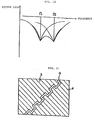
- the resonance frequencies of the two radiation electrodes are set so as to deviate from each other so that the frequency bands of transmitting and receiving waves of these two radiation electrodes partially overlap each other, as indicated by frequencies f1 and f2 in Fig. 10.
- By resonating the two radiation electrodes which thus slightly differ in the resonance frequency from each other, plural-resonance conditions in frequency characteristics as indicated by the solid line in Fig. 10 is created, whereby widening of the frequency bands of transmitting and receiving waves of the surface-mounted type antenna is realized.
- the present invention has been made in view of solving the above-described problems, and aims to present a surface-mounted type antenna of which the miniaturization and thinning has been realized, and which allows superior plural-resonance conditions to be achieved by adjusting the strength of the capacitive coupling between the two radiation electrodes, and aims further to present a communication device provided therewith.
- a surface-mounted type antenna in accordance with a first invention comprises a dielectric substrate, a first radiation electrode formed on the dielectric substrate, and a second radiation electrode disposed on the dielectric substrate at a predetermined distance from the first radiation electrode.
- capacitive-coupling adjusting means which makes the permittivity between the first radiation electrode and the second radiation electrode differ from that of the dielectric body, and which varies the strength of the capacitive coupling between the first radiation electrode and the second radiation electrode.
- a surface-mounted type antenna in accordance with a second invention has the construction of the first invention, and is characterized in that the capacitive-coupling adjusting means thereof is constituted of a recess or a groove in which a capacity occurs and which is formed between the first radiation electrode and the second radiation electrode, in the surface of the dielectric substrate.
- a surface-mounted type antenna in accordance with a third invention has the construction of the first invention, and is characterized in that a permittivity adjusting material portion which has a different permittivity from that of the dielectric substrate is interposed between the first radiation electrode and the second radiation electrode and that this permittivity adjusting material portion constitutes capacitive-coupling adjusting means.
- a surface-mounted type antenna in accordance with a fourth invention has the construction of the first invention, and is characterized in that the capacitive-coupling adjusting means is constituted of areas of the first radiation electrode and the second radiation electrode, the area being a hollow portion situated inside the dielectric substrate.
- a surface-mounted type antenna in accordance with a fifth invention comprises a dielectric substrate, a first radiation electrode formed on the surface of the dielectric substrate, and a second radiation electrode disposed on the surface of the dielectric substrate at a predetermined distance from the first radiation electrode.
- This surface-mounted type antenna is characterized in that the dielectric substrate is formed by bonding a first dielectric substrate and a second dielectric substrate which has a different permittivity from that of the first dielectric substrate, that the first radiation electrode is formed on the first dielectric substrate while the second radiation electrode is formed on the second dielectric substrate, and that the bonded portion between the first dielectric substrate and the second dielectric substrate is disposed in the space which is situated between the first radiation electrode and the second radiation electrode and in which a capacity occurs.
- a communication device in a sixth invention is characterized in that it is provided with a surface-mounted type antenna which has a construction of any one of the first through fifth inventions.
- the capacitive-coupling adjusting means makes the permittivity between the first radiation electrode and the second radiation electrode differ from that of the dielectric body.
- the strength of the capacitive coupling in the space which is situated between the first radiation electrode and the second radiation electrode and in which a capacity occurs varies in the "stronger” direction or in the "weaker” direction according to the permittivity between the first radiation electrode and the second radiation electrode, than the case where the permittivity between the first radiation electrode and the second radiation electrode is the permittivity of the dielectric substrate.
- the strength of the capacitive coupling in the space which is situated between the first radiation electrode and the second radiation electrode and in which a capacity occurs can be adjusted, it is possible to inhibit the mutual interference of the resonances of the first radiation electrode and the second radiation electrode, and to thereby improve antenna characteristics, while achieving the miniaturization and thinning of the surface-mounted type antenna.
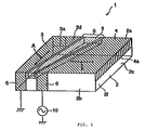
- Fig. 1 shows a schematic perspective view showing a surface-mounted type antenna in accordance with a first embodiment.
- the surface-mounted type antenna 1 shown in Fig. 1 has a dielectric substrate 2, and on the top surface 2a of the dielectric substrate 2, a power non-supplied side radiation electrode 3 which is a first radiating electrode, and a power supplied side radiation electrode 4 which is a second radiating electrode are formed with a space therebetween.
- the space S between the power non-supplied side radiation electrode 3 and the power supplied side radiation electrode 4 is formed so that the longitudinal sides thereof tilt with respect to each side of the top surface 2a of the dielectric substrate 2 (for example, at an angle of 45 degrees).
- a ground electrode 5 connected to the power non-supplied side radiation electrode 3, and a power supply electrode 6 connected to the power supply radiation side radiation electrode 4 are each linearly formed from the top surface side to the bottom surface side.
- the power supply radiation side radiation electrode 4 extends from the top surface 2a and forms the open end 4a thereof on a side surface 2c of the dielectric substrate 2, while the power non-supply radiation side radiation electrode 3 extends from the top surface 2a and forms the open end 3a thereof on a side surface 2d.
- the space S is formed so as to gradually widen from the side surface 2b, where the ground electrode 5 and the power supply electrode 6 are formed, toward the side surface 2d constituting an open end.
- the reason for this is as follows.
- the ground electrode 5 and the power supply electrode 6 are coupled in an electric field. Therefore, in order to effectively control the amount of the electric field coupling, it is effective to widen the space S on the open end, where a strong electric field exists, that is, the space S on the side surface 2d side.
- a permittivity adjusting material portion 8 which is the most characteristic capacitive-coupling adjusting means of the first embodiment is provided in the space S between the power non-supplied side radiation electrode 3 and the power supplied side radiation electrode 4.
- the purpose of providing the permittivity adjusting material portion 8 shown in the first embodiment is to weaken the capacitive coupling between the power non-supplied side radiation electrode 3 and the power supplied side radiation electrode 4.
- the permittivity adjusting material portion 8 has a lower permittivity than that of the dielectric substrate 2. In the example shown in Fig.
- the permittivity adjusting material portion 8 is embedded only in the upper side of the space S between the power non-supplied side radiation electrode 3 and the power supplied side radiation electrode 4, in the dielectric substrate 2 (that is, only in the area chiefly concerned to the capacity between the power non-supplied side radiation electrode 3 and the power supplied side radiation electrode 4).
- the surface-mounted type antenna in according with the first embodiment has the features as described above.
- a surface-mounted type antenna 1 is mounted onto the circuit board incorporated in a communication device such as portable telephone or the like, in such a manner in which the bottom 2f of the dielectric substrate 2 is mounted on the circuit board side.
- the circuit board has a power supply circuit 10 formed thereon. By mounting the surface-mounted type antenna 1 onto the circuit board, the power supply electrode 6 of the surface-mounted type antenna 1 is connected to the power supply circuit 10.
- the power When a power is supplied from the power supply circuit 10 to the power supply electrode 6, the power is directly supplied from the power supply electrode 6 to the power supplied side radiation electrode 4, and the power is transmitted by the power supply electrode 6 to the power non-supplied side radiation electrode 3 by virtue of electromagnetic coupling, whereby the power non-supplied side radiation electrode 3 and the power supplied side radiation electrode 4 resonate and perform the function of an antenna.
- the longitudinal sides of the space S between the power non-supplied side radiation electrode 3 and the power supplied side radiation electrode 4 tilt with respect to each side of the top surface 2a of the dielectric substrate 2, and the ground electrode 5 and the power supply electrode 6 are disposed adjacent to each other, as well as the open end 3a of the power non-supplied side radiation electrode 3 and the open end 4a of the power supplied side radiation electrode 4 are formed on the different side surfaces from each other, of the dielectric substrate 2.
- the mutual interference of the resonances of the power non-supplied side radiation electrode 3 and the power supplied side radiation electrode 4 can be substantially inhibited, by arranging the resonance direction A of the power non-supplied side radiation electrode 3 and the resonance direction B of the power supplied side radiation electrode 4 so as to intersect each other substantially at right angles.
- the above-described arrangement cannot achieve by itself the capacity between the power non-supplied side radiation electrode 3 and the power supplied side radiation electrode 4, the capacity being commensurate with the capacity (fringing capacity) between the power non-supplied side radiation electrode 3 and the ground or the capacity (fringing capacity) between the power supplied side radiation electrode 4 and the ground. This results in that a mutual interference of the resonances between the power non-supplied side radiation electrode 3 and the power supplied side radiation electrode 4 cannot be completely inhibited.
- the permittivity adjusting material portion 8 which has a lower permittivity than that of the dielectric substrate 2 is interposed between the power non-supplied side radiation electrode 3 and the power supplied side radiation electrode 4, in this first embodiment, as described above, so that the capacity occurring between the power non-supplied side radiation electrode 3 and the power supplied side radiation electrode 4 can be made smaller than the case where the entire area between the power non-supplied side radiation electrode 3 and the power supplied side radiation electrode 4 is the dielectric substrate 2. This allows the capacitive coupling between the power non-supplied side radiation electrode 3 and the power supplied side radiation electrode 4 to be significantly weakened.
- the control of the amount of the capacitive coupling between the power non-supplied side radiation electrode 3 and the power supplied side radiation electrode 4 can be effectively performed, in conjunction with the adjustment of the capacitive coupling by the permittivity adjusting material portion 8.
- This second embodiment characteristically differs from the above-described first embodiment in that, as shown in Fig. 2, there is provided a groove 12 which is capacity coupling means, instead of the permittivity adjusting material portion 8 provided between the power non-supplied side radiation electrode 3 and the power supplied side radiation electrode 4.
- a groove 12 which is capacity coupling means, instead of the permittivity adjusting material portion 8 provided between the power non-supplied side radiation electrode 3 and the power supplied side radiation electrode 4.
- Other features are the same as those of the first embodiment.
- the same components as those of the first embodiment have been given the same reference numerals, and repeated descriptions of the components in common therebetween will be omitted.
- the surface-mounted type antenna in accordance with the second embodiment is also provided with an arrangement for weakening the capacitive coupling between the power non-supplied side radiation electrode 3 and the power supplied side radiation electrode 4, as in the case of the first embodiment.
- the groove 12 which characterizes this second embodiment is provide along the longitudinal sides of the space S between the power non-supplied side radiation electrode 3 and the power supplied side radiation electrode 4, and the magnitude of the groove 12 is one enough to reduce the permittivity between the power non-supplied side radiation electrode 3 and the power supplied side radiation electrode 4 to a small value such as to inhibit the mutual interference of the resonances of the power non-supplied side radiation electrode 3 and the power supplied side radiation electrode 4.
- the power non-supplied side radiation electrode 3 and the power supplied side radiation electrode 4 are formed so as to intersect each other substantially at right angles, as in the case of the first embodiment.
- the groove 12 is formed between the power non-supplied side radiation electrode 3 and the power supplied side radiation electrode 4, whereby the permittivity between the power non-supplied side radiation electrode 3 and the power supplied side radiation electrode 4 is made lower than that of the dielectric substrate 2, and thereby the capacitive coupling between the power non-supplied side radiation electrode 3 and the power supplied side radiation electrode 4 is weakened.
- this second embodiment also, it is possible to reliably inhibit the mutual interference of the resonances of the power non-supplied side radiation electrode 3 and the power supplied side radiation electrode 4, and to stably achieve superior plural-resonance conditions, as is the case with the first embodiment.
- This can produce superior effects which allow a surface-mounted type antenna 1 which is small and low-profile and which has high-reliability antenna characteristics to be provided.
- This third embodiment is characterized in that, as shown in Fig. 3, hollow portions 14 and 15 as capacitive-coupling adjusting means are provided within the dielectric substrate 2.
- Other features are the same as those of the above-described embodiments.
- the same components as those of the above-described embodiments have been given the same reference numerals, and repeated descriptions of components in common therebetween will be omitted.
- the hollow portion 14 is located in the area of the power non-supplied side radiation electrode 3, within the dielectric substrate 2, while the hollow portion 15 is provided together with the hollow portion 14 at a distance therefrom.
- the hollow portion 14 since the hollow portion 14 is formed in the area of the power non-supplied side radiation electrode 3, within the dielectric substrate 2, the hollow portion 14 allows the capacity between the power non-supplied side radiation electrode 3 and the ground to be reduced. Also, since the hollow portion 15 is formed in the area of the power supplied side radiation electrode 4, within the dielectric substrate 2, the hollow portion 15 allows the capacity between the power supplied side radiation electrode 4 and the ground to be reduced.
- each of the fringing capacities between the radiation electrodes 3 and 4 and the ground can be easily varied so as to be commensurate with the capacity between the power non-supplied side radiation electrode 3 and the power supplied side radiation electrode 4, it is possible to adjust the capacity between the power non-supplied side radiation electrode 3 and the power supplied side radiation electrode 4 and the above-described fringing capacity so as to have an proper relationship of being commensurate with each other.
- the hollow portion 14 is located adjacent to the open end 3a of the power non-supplied side radiation electrode 3, and the hollow portion 15 is formed adjacent to the open end 4a of the power supplied side radiation electrode 4, it is possible to reduce the permittivity between the power non-supplied side radiation electrode 3 and the ground, and that between the power supplied side radiation electrode 4 and the ground, and is thereby possible to relieve the electric field concentration between the power non-supplied side radiation electrode 3 and the ground and that between the power supplied side radiation electrode 4 and the ground.
- This effect coupled with the suppressing effect with respect to the mutual interference of the resonances between the power non-supplied side radiation electrode 3 and the power supplied side radiation electrode 4, can promote widening of the band width of the surface-mounted type antenna 1 and an increase in the gain thereof.
- the fourth embodiment is characterized in that, as is the cases with the above-described embodiments, there is provided an arrangement for weakening the capacitive coupling between the power non-supplied side radiation electrode 3 and the power supplied side radiation electrode 4.
- the dielectric substrate 2 is formed by bonding first and second dielectric substrates 17 and 18 which have different permittivities from each other, and the bonded portion 20 between the first dielectric substrate 17 and the second dielectric substrate 18 is disposed in the space S between the power non-supplied side radiation electrode 3 and the power supplied side radiation electrode 4.
- Other features are substantially the same as those of the above-described embodiments.
- the same components as those of the above-described embodiments have been given the same reference numerals, and repeated descriptions of components in common therebetween will be omitted.
- the second dielectric substrate 18 has a lower permittivity than that of the first dielectric substrate 17, and the first dielectric substrate 17 and the second dielectric substrate 18 are bonded by, for example, a ceramic adhesive.
- a power non-supplied side radiation electrode 3 is formed on the surface of the first dielectric substrate 17, while a power supplied side radiation electrode 4 is formed on the surface of the second dielectric substrate 18.
- a dielectric substrate 2 is formed by bonding the first dielectric substrate 17 for forming the power non-supplied side radiation electrode 3 and the second dielectric substrate 18 for forming the power supplied side radiation electrode 4, the radiation electrodes 3 and 4 having different permittivities from each other.
- the bonded portion 20 between the first dielectric substrate 17 and the second dielectric substrate 18 is disposed in the space S between the power non-supplied side radiation electrode 3 and the power supplied side radiation electrode 4. That is, the first and second dielectric substrates 17 and 18 which have different permittivities from each other, are disposed between the power non-supplied side radiation electrode 3 and the power supplied side radiation electrode 4.
- the capacity between the power non-supplied side radiation electrode 3 and the power supplied side radiation electrode 4 is, of course, related to the occupation ratio between the first dielectric substrate 17 and the second dielectric substrate 18 in between the power non-supplied side radiation electrode 3 and the power supplied side radiation electrode 4, but it is primarily determined based on the permittivity of the dielectric substrate having the lower permittivity.
- the bonded portion 20 between the first dielectric substrate 17 and the second dielectric substrate 18 is disposed at the position which allows the capacitive coupling between the power non-supplied side radiation electrode 3 and the power supplied side radiation electrode 4 to be weakened, and which thereby enables the mutual interference of the resonances between the power non-supplied side radiation electrode 3 and the power supplied side radiation electrode 4 to be inhibited.
- the dielectric substrate 2 is formed by bonding the first and second dielectric substrates 17 and 18 which have different permittivities from each other, and the bonded portion 20 between the first dielectric substrate 17 and the second dielectric substrate 18 is disposed in the space S between the power non-supplied side radiation electrode 3 and the power supplied side radiation electrode 4.
- Providing this construction allows the capacity between the power non-supplied side radiation electrode 3 and the power supplied side radiation electrode 4 to be reduced, and enables the mutual interference of the resonances between the power non-supplied side radiation electrode 3 and the power supplied side radiation electrode 4 to be suppressed, with the result that superior plural-resonance conditions are stably achieved.
- This can produce superior effects which allow a surface-mounted type antenna 1 which is small and low-profile and which has high-reliability antenna characteristics to be provided.
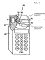
- FIG. 5 schematically illustrates an example of a portable telephone which is a communication device.
- the portable telephone 25 shown in Fig. 5 has a circuit board 27 provided in a case 26.
- a power supply circuit 10, a switching circuit 30, a transmitting circuit 31, and a receiving circuit 32 are formed on the circuit board 27.
- the surface-mounted type antenna 1 performs the function of an antenna by receiving the supply of a power from the power supply circuit 10 thereto, as described above, and the transmission and reception of waves are smoothly performed by the switching action of the switching circuit 30.
- the portable telephone 25 since the portable telephone 25 is equipped with one of the surface-mounted type antennas 1 shown in the above-described embodiments, the miniaturization of the portable telephone 25 can be easily achieved as a result of the size-reduction of the surface-mounted type antenna 1. Also, a portable telephone 25 having a high reliability of communication can be provided since it incorporates therein a surface-mounted type antenna 1 having superior antenna characteristics as described above.
- the present invention is not limited to the above-described embodiments, but various embodiments can be adopted.
- the shapes of the power non-supplied side radiation electrode 3 and the power supplied side radiation electrode 4 are not restricted to the shapes illustrated in the above-described embodiments, but various shapes can be used.
- the shapes as shown in Figs. 6(a), 6(b) and 7(a) can be employed.
- the power non-supplied side radiation electrode 3 and the power supplied side radiation electrode 4 are formed into a meander-shape.
- the arrangement is such that a power is transmitted from an meander-shaped end portion ⁇ to the power non-supplied side radiation electrode 3, while a power is transmitted from an meander-shaped end portion ⁇ to the power supplied side radiation electrode 4.
- the open end of the power non-supplied side radiation electrode 3 is formed on a side surface 2e of the dielectric substrate 2, while the open end of the power supplied side radiation electrode 4 is formed on a side surface 2c.
- the example shown in Fig. 6(b) is the one wherein the electrode area on the open end side of the power supplied side radiation electrode 4 shown in Fig. 6(a) is enlarged, and wherein the electric field concentration on the open end side of the power supplied side radiation electrode 4 is thereby relieved in order to further improve the antenna characteristics.
- Fig. 7(a) are shape examples of the power non-supplied side radiation electrode 3 and the power supplied side radiation electrode 4 which allow the above-described plural resonance to be created in a dual-band surface-mounted type antenna 1 which is capable of transmitting and receiving waves in two different frequency bands from each other, as shown in the frequency characteristics in Fig. 7(b) and 7(c).
- Fig. 7(b) and 7(c) the frequency characteristics in Fig. 7(b) and 7(c).
- the arrangement is such that the power non-supplied side radiation electrode 3 and the power supplied side radiation electrode 4 are each formed into meander-shapes, that an electrode is transmitted to each of the meander-shaped end portions ⁇ and ⁇ of the power non-supplied side radiation electrode 3 and the power supplied side radiation electrode 4, and that the resonance direction A of the power non-supplied side radiation electrode 3 and the resonance direction B of the power supplied side radiation electrode 4 intersect each other at substantially at right angles.
- the power supplied side radiation electrode 4 is formed by continuously connecting a plurality of electrode portions 4a and 4b which differ in the meander pitch from each other, and is formed so as to have two resonance frequencies F1 and F2 such that the frequency bands of waves do not overlap each other, as illustrated in Figs. 7(b) and 7(c).
- the resonance frequency of the power non-supplied side radiation electrode 3 is set to a frequency in the vicinity of the resonance frequency F1 of the power supplied side radiation electrode 4, or to a frequency in the vicinity of the above-described resonance frequency F2 so as to have a plural-resonance relation with the resonance frequency of the power supplied side radiation electrode 4.
- the resonance frequency of the power non-supplied side radiation electrode 3 is set to a frequency in the vicinity of the resonance frequency F1 of the power supplied side radiation electrode 4, for example, to the frequency F1' shown in Fig. 7(b), a plural-resonance state is created at the resonance frequency F1, while, when the resonance frequency of the power non-supplied side radiation electrode 3 is set to a frequency in the vicinity of the resonance frequency F2 of the power supplied side radiation electrode 4, for example, to the frequency F2' shown in Fig. 7(c), a plural-resonance state is created at the resonance frequency F2.
- a permittivity adjusting material portion 8 or a groove 12 is provided, for example, as indicated by the dot lines in Figs. 6(a), 6(b), or 7(a).
- the dielectric substrate 2 is formed by bonding the first dielectric substrate 17 which is used for forming the power non-supplied side radiation electrode 3, and the second dielectric substrate 18 which has a lower permittivity and which is used for forming the power supplied side radiation electrode 4, for example, as shown in Figs. 8(a) and 8(b).
- the arrangement is such that a power is directly supplied from the power supply electrode 6 to the power supplied side radiation electrode 4, but it may be such that the power supplied side radiation electrode 4 and the power supply electrode 6 is non-connected to each other, and that a power is supplied from the power supply electrode 6 to the power supplied side radiation electrode 4 by means of capacitive coupling.
- the width of the permittivity adjusting material portion 8 is narrower than that of the space S between the power non-supplied side radiation electrode 3 and the power supplied side radiation electrode 4.
- the width of permittivity adjusting material portion 8 may be arranged so as to be wider than that of the space S so that the power non-supplied side radiation electrode 3 and the power supplied side radiation electrode 4 are formed astride the edge portions of the permittivity adjusting material portion 8.
- the groove 12 is provided in the space S between the power non-supplied side radiation electrode 3 and the power supplied side radiation electrode 4, but, for example, a recess without an opening may be formed on the side surfaces 2b and 2d, instead of the groove 12. Furthermore, a plurality of recesses as capacitive-coupling adjusting means may be arranged with a space therebetween.
- the two hollow portions 14 and 15 are provided, but only one of these hollow portions 14 and 15 may be formed.
- the shape of the hollow portions 14 and 15 is not limited to the one shown in Fig. 3, but various shapes may be adopted.
- the hollow portions 14 and 15 shown in Fig. 3 pass through the dielectric substrate from the side surface 2b to the side surface 2d, but they may be closed hollow portions without openings.
- the hollow portions 14 and 15 may be recesses or groove-shaped hollow portions such that the bottom 2f side of the dielectric substrate 2 is open.
- the construction wherein a permittivity adjusting material portion is provided as shown in the first embodiment
- the construction wherein a groove or a recess is provided as shown in the second embodiment
- the construction wherein hollow portions are provided as shown in the third embodiment
- the construction wherein the dielectric substrate 2 constitutes a bonded body of a plurality of dielectric substrates which differ in the permittivity from each other as shown in the fourth embodiment, two or more constructions may be combined to use.
- capacitive-coupling adjusting means for strengthening the capacitive coupling between the power non-supplied side radiation electrode 3 and the power supplied side radiation electrode 4.
- capacitive-coupling adjusting means for strengthening the capacitive coupling between the power non-supplied side radiation electrode 3 and the power supplied side radiation electrode 4.
- the following permittivity adjusting material portion 8 as capacitive-coupling adjusting means is provided in the space S between the power non-supplied side radiation electrode 3 and the power supplied side radiation electrode 4.
- This permittivity adjusting material portion 8 is formed of a material having a higher permittivity than that of the dielectric substrate 2.
- the power non-supplied side radiation electrode 3 and the power supplied side radiation electrode 4 may be formed into shapes as shown in Fig. 11 so that the space S between the power non-supplied side radiation electrode 3 and the power supplied side radiation electrode 4 is narrowed, and that the capacity between the power non-supplied side radiation electrode 3 and the power supplied side radiation electrode 4 is increased so as to become a capacity which is commensurate with that of the above-described fringing capacity, by enlarging the areas of the opposing electrodes.
- the capacity between the power non-supplied side radiation electrode 3 and the power supplied side radiation electrode 4 is significantly smaller than the fringing capacity
- the capacity between the power non-supplied side radiation electrode 3 and the power supplied side radiation electrode 4 and the fringing capacity can be brought into a proper matching relation, by adjusting the capacity between the power non-supplied side radiation electrode 3 and the power supplied side radiation electrode 4 to increase so as to become a capacity which is commensurate with the fringing capacity by means of the above-described capacitive-coupling adjusting means for increasing the capacity between the power non-supplied side radiation electrode 3 and the power supplied side radiation electrode 4.
- the power non-supplied side radiation electrode 3 and the power supplied side radiation electrode 4 may be formed within the dielectric substrate 2.
- the dielectric substrate 2 a multilayer substrate formed by laminating a plurality of ceramic green sheets may be used. Ceramic green sheets having a different permittivity from that of the above-mentioned ceramic sheets may be provided between the power non-supplied side radiation electrode 3 and the power supplied side radiation electrode 4, for use as capacitive- coupling adjusting means.
- capacitive-coupling adjusting means when capacitive-coupling adjusting means is provided, and the strength of the capacitive coupling between the first radiation electrode and the second radiation electrode is varied by making the permittivity in the space which is situated between the first radiation electrode and the second radiation electrode and in which a capacity occurs, differ from that of the dielectric substrate by means of the above-described capacitive-coupling adjusting means, the mutual interference of the resonances between the first radiation electrode and the second radiation electrode can be inhibited.
- the strength of the capacitive coupling between the first radiation electrode and the second radiation electrode can be varied by a simple construction, whereby superior effects as described above are produced.
- the dielectric substrate constitutes a bonded body of the first dielectric substrate and the second dielectric substrate which differ in the permittivity from each other
- the first radiation electrode is formed on the first dielectric substrate while the second radiation electrode is formed on the second dielectric substrate, and a bonded portion between the first dielectric substrate and the second dielectric substrate is provided between the first radiation electrode and the second radiation electrode, it is possible to vary the permittivity between the first radiation electrode and the second radiation electrode, as in the case described above.
- This allows the mutual interference of the resonances between the first radiation electrode and the second radiation electrode to be suppressed, and enables a surface-mounted type antenna which is small and low-profile and which has high-reliability antenna characteristics to be provided.
- the degree of freedom of design can be improved.
- the surface-mounted type antenna and the communication device provided therewith are applied to, for example, surface-mounted type antennas and the like to be mounted on the circuit boards incorporated in communication devices such as portable telephones.
Landscapes
- Engineering & Computer Science (AREA)
- Computer Networks & Wireless Communication (AREA)
- Microelectronics & Electronic Packaging (AREA)
- Details Of Aerials (AREA)
- Waveguide Aerials (AREA)
- Support Of Aerials (AREA)
- Aerials With Secondary Devices (AREA)
Abstract
Description
Claims (9)
- A surface-mounted type antenna comprising:wherein:a dielectric substrate;a first radiation electrode formed on said dielectric substrate; anda second radiation electrode disposed on said dielectric substrate at a predetermined distance from said first radiation electrode,
capacitive-coupling adjusting means is provided which make the permittivity between said first radiation electrode and said second radiation electrode differ from that of said dielectric body, and which varies the strength of the capacitive coupling between said first radiation electrode and said second radiation electrode. - A surface-mounted type antenna as claimed in claim 1, wherein:
said first radiation electrode and said second radiation electrode are formed on the surface of said dielectric substrate. - A surface-mounted type antenna as claimed in claim 1, wherein:
said capacitive-coupling adjusting means is constituted of a recess or a groove formed between said first radiation electrode and said second radiation electrode, in the surface of the dielectric substrate. - A surface-mounted type antenna as claimed in claim 1, wherein:a permittivity adjusting material portion which has a different permittivity from that of the dielectric substrate is interposed between said first radiation electrode and said second radiation electrode; andsaid permittivity adjusting material portion constitutes capacitive-coupling adjusting means.
- A surface-mounted type antenna as claimed in claim 1, wherein:
said capacitive-coupling adjusting means is constituted of an area between said first radiation electrode and said second radiation electrode, said area being a hollow portion situated inside said dielectric substrate. - A surface-mounted type antenna as claimed in claim 1, wherein:
said first radiation electrode and said second radiation electrode are formed so that the resonance directions thereof are substantially orthogonal to each other. - A surface-mounted type antenna comprising:wherein:a dielectric substrate;a first radiation electrode formed on the surface of said dielectric substrate; anda second radiation electrode disposed on the surface of said dielectric substrate at a predetermined distance from said first radiation electrode,said dielectric substrate is formed by bonding a first dielectric substrate and a second dielectric substrate which has a different permittivity from that of said first dielectric substrate;said first radiation electrode is formed on said first dielectric substrate, and said second radiation electrode is formed on said second dielectric substrate; andthe bonded portion between said first dielectric substrate and said second dielectric substrate is disposed between the first radiation electrode and the second radiation electrode.
- A surface-mounted type antenna as claimed in claim 7, wherein:
said first radiation electrode and said second radiation electrode are formed so that the resonance directions thereof are substantially orthogonal to each other. - A communication device comprising a surface-mounted type antenna as claimed in any one of claims 1 through 7.
Applications Claiming Priority (3)
| Application Number | Priority Date | Filing Date | Title |
|---|---|---|---|
| JP25555199 | 1999-09-09 | ||
| JP25555199 | 1999-09-09 | ||
| PCT/JP2000/006158 WO2001018909A1 (en) | 1999-09-09 | 2000-09-08 | Surface-mount antenna and communication device with surface-mount antenna |
Publications (3)
| Publication Number | Publication Date |
|---|---|
| EP1139490A1 true EP1139490A1 (en) | 2001-10-04 |
| EP1139490A4 EP1139490A4 (en) | 2004-03-24 |
| EP1139490B1 EP1139490B1 (en) | 2007-02-07 |
Family
ID=17280306
Family Applications (1)
| Application Number | Title | Priority Date | Filing Date |
|---|---|---|---|
| EP00957060A Expired - Lifetime EP1139490B1 (en) | 1999-09-09 | 2000-09-08 | Surface-mount antenna and communication device with surface-mount antenna |
Country Status (8)
| Country | Link |
|---|---|
| US (1) | US6501425B1 (en) |
| EP (1) | EP1139490B1 (en) |
| JP (1) | JP3596526B2 (en) |
| KR (1) | KR100432100B1 (en) |
| CN (1) | CN1151588C (en) |
| CA (2) | CA2426497C (en) |
| DE (1) | DE60033275T2 (en) |
| WO (1) | WO2001018909A1 (en) |
Cited By (15)
| Publication number | Priority date | Publication date | Assignee | Title |
|---|---|---|---|---|
| EP1128466A3 (en) * | 2000-02-24 | 2003-09-17 | Filtronic LK Oy | Planar antenna structure |
| AU2003204642B2 (en) * | 2002-06-27 | 2004-06-10 | Harris Corporation | Dipole arrangements using dielectric substrates of meta-materials |
| EP1530256A1 (en) * | 2003-11-06 | 2005-05-11 | YOKOWO Co., Ltd | Multi-frequency antenna |
| WO2006000650A1 (en) * | 2004-06-28 | 2006-01-05 | Pulse Finland Oy | Antenna component |
| WO2006097567A1 (en) * | 2005-03-16 | 2006-09-21 | Pulse Finland Oy | Antenna component |
| EP2081255A1 (en) | 2008-01-15 | 2009-07-22 | TDK Corporation | Surface mount antenna and antenna module |
| US7679565B2 (en) | 2004-06-28 | 2010-03-16 | Pulse Finland Oy | Chip antenna apparatus and methods |
| EP2128927A4 (en) * | 2007-02-01 | 2010-12-01 | Fujitsu Semiconductor Ltd | ANTENNA |
| US7889143B2 (en) | 2005-10-03 | 2011-02-15 | Pulse Finland Oy | Multiband antenna system and methods |
| US7903035B2 (en) | 2005-10-10 | 2011-03-08 | Pulse Finland Oy | Internal antenna and methods |
| US7916086B2 (en) | 2004-11-11 | 2011-03-29 | Pulse Finland Oy | Antenna component and methods |
| US8378892B2 (en) | 2005-03-16 | 2013-02-19 | Pulse Finland Oy | Antenna component and methods |
| US9673507B2 (en) | 2011-02-11 | 2017-06-06 | Pulse Finland Oy | Chassis-excited antenna apparatus and methods |
| US9917346B2 (en) | 2011-02-11 | 2018-03-13 | Pulse Finland Oy | Chassis-excited antenna apparatus and methods |
| US10211538B2 (en) | 2006-12-28 | 2019-02-19 | Pulse Finland Oy | Directional antenna apparatus and methods |
Families Citing this family (73)
| Publication number | Priority date | Publication date | Assignee | Title |
|---|---|---|---|---|
| EP1223637B1 (en) | 1999-09-20 | 2005-03-30 | Fractus, S.A. | Multilevel antennae |
| GB0105251D0 (en) | 2001-03-02 | 2001-04-18 | Nokia Mobile Phones Ltd | Antenna |
| EP1239539A3 (en) * | 2001-03-02 | 2003-11-05 | Nokia Corporation | Antenna |
| DE10113349A1 (en) * | 2001-03-20 | 2002-09-26 | Philips Corp Intellectual Pty | Antenna with substrate and conducting track has at least one aperture formed by hollow chamber enclosed by substrate or by recess formed in one or more surfaces of substrate |
| JP3678167B2 (en) | 2001-05-02 | 2005-08-03 | 株式会社村田製作所 | ANTENNA DEVICE AND RADIO COMMUNICATION DEVICE HAVING THE ANTENNA DEVICE |
| US6759984B2 (en) * | 2001-06-01 | 2004-07-06 | Agere Systems Inc. | Low-loss printed circuit board antenna structure and method of manufacture thereof |
| JP3649168B2 (en) * | 2001-08-07 | 2005-05-18 | 株式会社村田製作所 | RF circuit integrated antenna, antenna module using the same, and communication device including the same |
| JP2003283239A (en) * | 2002-03-20 | 2003-10-03 | Mitsubishi Electric Corp | Antenna device |
| US6720926B2 (en) | 2002-06-27 | 2004-04-13 | Harris Corporation | System for improved matching and broadband performance of microwave antennas |
| KR100626667B1 (en) * | 2002-08-28 | 2006-09-22 | 한국전자통신연구원 | Planar Inverted F Antenna |
| JP2004096259A (en) * | 2002-08-30 | 2004-03-25 | Matsushita Electric Ind Co Ltd | Multi-frequency microstrip antenna |
| JP2004128605A (en) * | 2002-09-30 | 2004-04-22 | Murata Mfg Co Ltd | Antenna structure and communication system therewith |
| JP2005012743A (en) | 2002-10-22 | 2005-01-13 | Matsushita Electric Ind Co Ltd | Antenna and electronic equipment using it |
| US6762723B2 (en) * | 2002-11-08 | 2004-07-13 | Motorola, Inc. | Wireless communication device having multiband antenna |
| WO2005013418A1 (en) * | 2003-08-01 | 2005-02-10 | Sanyo Electric Co., Ltd. | Patch antenna |
| US7382319B2 (en) | 2003-12-02 | 2008-06-03 | Murata Manufacturing Co., Ltd. | Antenna structure and communication apparatus including the same |
| CN1938902B (en) | 2004-03-31 | 2012-05-30 | Toto株式会社 | Microstrip antenna |
| JP3895737B2 (en) | 2004-04-09 | 2007-03-22 | 古河電気工業株式会社 | Multi-frequency antenna and small antenna |
| FI20055420A0 (en) | 2005-07-25 | 2005-07-25 | Lk Products Oy | Adjustable multi-band antenna |
| FI119009B (en) | 2005-10-03 | 2008-06-13 | Pulse Finland Oy | Multiple-band antenna |
| FI118782B (en) | 2005-10-14 | 2008-03-14 | Pulse Finland Oy | Adjustable antenna |
| US8618990B2 (en) | 2011-04-13 | 2013-12-31 | Pulse Finland Oy | Wideband antenna and methods |
| US8738103B2 (en) | 2006-07-18 | 2014-05-27 | Fractus, S.A. | Multiple-body-configuration multimedia and smartphone multifunction wireless devices |
| US20080062045A1 (en) * | 2006-09-08 | 2008-03-13 | Motorola, Inc. | Communication device with a low profile antenna |
| US7545330B2 (en) * | 2006-12-04 | 2009-06-09 | Kabushiki Kaisha Toshiba | Antenna device including surface-mounted element |
| EP2104178A4 (en) * | 2007-01-19 | 2014-05-28 | Murata Manufacturing Co | Antenna unit and wireless communication apparatus |
| FI20075269A0 (en) | 2007-04-19 | 2007-04-19 | Pulse Finland Oy | Method and arrangement for antenna matching |
| CN101299482B (en) * | 2007-05-01 | 2012-09-05 | 佛山市顺德区顺达电脑厂有限公司 | Antenna structure of built-in resonant circuit |
| WO2008136244A1 (en) | 2007-05-02 | 2008-11-13 | Murata Manufacturing Co., Ltd. | Antenna structure and wireless communication apparatus comprising the same |
| FI120427B (en) | 2007-08-30 | 2009-10-15 | Pulse Finland Oy | Adjustable multiband antenna |
| KR100906359B1 (en) * | 2007-09-28 | 2009-07-06 | (주)에이스안테나 | Composite ceramic antenna with heterogeneous dielectric |
| US20090091504A1 (en) * | 2007-10-04 | 2009-04-09 | Zylaya Corporation | Low-profile feed-offset wideband antenna |
| CN101911385B (en) * | 2008-01-17 | 2013-04-03 | 株式会社村田制作所 | Antenna |
| CN101582536B (en) * | 2008-05-16 | 2010-11-17 | 云南银河之星科技有限公司 | Antenna |
| JPWO2010023752A1 (en) * | 2008-08-29 | 2012-01-26 | パイオニア株式会社 | Longitudinal antenna |
| JP4775423B2 (en) * | 2008-09-24 | 2011-09-21 | Tdk株式会社 | Antenna device |
| JP4784636B2 (en) * | 2008-10-28 | 2011-10-05 | Tdk株式会社 | Surface mount antenna, antenna device using the same, and radio communication device |
| FI20096134A0 (en) | 2009-11-03 | 2009-11-03 | Pulse Finland Oy | Adjustable antenna |
| FI20096251A0 (en) | 2009-11-27 | 2009-11-27 | Pulse Finland Oy | MIMO antenna |
| CN201752032U (en) * | 2009-12-16 | 2011-02-23 | 中兴通讯股份有限公司 | Terminal antenna for feeding based on coupling feed way |
| US8847833B2 (en) | 2009-12-29 | 2014-09-30 | Pulse Finland Oy | Loop resonator apparatus and methods for enhanced field control |
| FI20105158A7 (en) | 2010-02-18 | 2011-08-19 | Pulse Finland Oy | ANTENNA EQUIPPED WITH SHELL RADIATOR |
| US9406998B2 (en) | 2010-04-21 | 2016-08-02 | Pulse Finland Oy | Distributed multiband antenna and methods |
| JP2012023640A (en) * | 2010-07-15 | 2012-02-02 | Tdk Corp | Antenna device |
| TW201216555A (en) * | 2010-10-12 | 2012-04-16 | Hon Hai Prec Ind Co Ltd | Antenna |
| FI20115072A0 (en) | 2011-01-25 | 2011-01-25 | Pulse Finland Oy | Multi-resonance antenna, antenna module and radio unit |
| US8866689B2 (en) | 2011-07-07 | 2014-10-21 | Pulse Finland Oy | Multi-band antenna and methods for long term evolution wireless system |
| US9450291B2 (en) | 2011-07-25 | 2016-09-20 | Pulse Finland Oy | Multiband slot loop antenna apparatus and methods |
| US9123990B2 (en) | 2011-10-07 | 2015-09-01 | Pulse Finland Oy | Multi-feed antenna apparatus and methods |
| US9531058B2 (en) | 2011-12-20 | 2016-12-27 | Pulse Finland Oy | Loosely-coupled radio antenna apparatus and methods |
| US9484619B2 (en) | 2011-12-21 | 2016-11-01 | Pulse Finland Oy | Switchable diversity antenna apparatus and methods |
| JP6033560B2 (en) | 2012-03-16 | 2016-11-30 | Ntn株式会社 | Multiband antenna and manufacturing method thereof |
| US8988296B2 (en) | 2012-04-04 | 2015-03-24 | Pulse Finland Oy | Compact polarized antenna and methods |
| WO2014021082A1 (en) * | 2012-08-03 | 2014-02-06 | 株式会社村田製作所 | Antenna apparatus |
| US9979078B2 (en) | 2012-10-25 | 2018-05-22 | Pulse Finland Oy | Modular cell antenna apparatus and methods |
| US10069209B2 (en) | 2012-11-06 | 2018-09-04 | Pulse Finland Oy | Capacitively coupled antenna apparatus and methods |
| US10079428B2 (en) | 2013-03-11 | 2018-09-18 | Pulse Finland Oy | Coupled antenna structure and methods |
| US9647338B2 (en) | 2013-03-11 | 2017-05-09 | Pulse Finland Oy | Coupled antenna structure and methods |
| US9634383B2 (en) | 2013-06-26 | 2017-04-25 | Pulse Finland Oy | Galvanically separated non-interacting antenna sector apparatus and methods |
| US9680212B2 (en) | 2013-11-20 | 2017-06-13 | Pulse Finland Oy | Capacitive grounding methods and apparatus for mobile devices |
| US9590308B2 (en) | 2013-12-03 | 2017-03-07 | Pulse Electronics, Inc. | Reduced surface area antenna apparatus and mobile communications devices incorporating the same |
| US9350081B2 (en) | 2014-01-14 | 2016-05-24 | Pulse Finland Oy | Switchable multi-radiator high band antenna apparatus |
| CN103811867A (en) * | 2014-02-25 | 2014-05-21 | 联想(北京)有限公司 | Antenna and terminal |
| US9973228B2 (en) | 2014-08-26 | 2018-05-15 | Pulse Finland Oy | Antenna apparatus with an integrated proximity sensor and methods |
| US9948002B2 (en) | 2014-08-26 | 2018-04-17 | Pulse Finland Oy | Antenna apparatus with an integrated proximity sensor and methods |
| US9722308B2 (en) | 2014-08-28 | 2017-08-01 | Pulse Finland Oy | Low passive intermodulation distributed antenna system for multiple-input multiple-output systems and methods of use |
| JP6447916B2 (en) * | 2015-03-20 | 2019-01-09 | 三菱マテリアル株式会社 | ANTENNA DEVICE AND COMMUNICATION DEVICE HAVING THE SAME |
| US9906260B2 (en) | 2015-07-30 | 2018-02-27 | Pulse Finland Oy | Sensor-based closed loop antenna swapping apparatus and methods |
| EP3480894A4 (en) * | 2016-06-30 | 2020-03-04 | Hitachi Metals, Ltd. | PLANE ANTENNA, COOKED CERAMIC SUBSTRATE, AND QUASI-MILLIMETER / MILLIMETER WAVE WIRELESS COMMUNICATION MODULE |
| CN108417970B (en) * | 2018-02-28 | 2020-10-27 | 深圳创维无线技术有限公司 | Multi-frequency built-in antenna and wireless terminal |
| KR102049755B1 (en) | 2018-07-27 | 2019-11-28 | 주식회사 에이스테크놀로지 | Multi-band antenna using button device and communication terminal |
| US10862211B2 (en) * | 2018-08-21 | 2020-12-08 | Htc Corporation | Integrated antenna structure |
| CN114389005B (en) * | 2020-10-19 | 2023-07-28 | 华为技术有限公司 | an electronic device |
Family Cites Families (27)
| Publication number | Priority date | Publication date | Assignee | Title |
|---|---|---|---|---|
| JPS6058704A (en) * | 1983-09-09 | 1985-04-04 | Nippon Telegr & Teleph Corp <Ntt> | Double resonance type inverted-f antenna |
| JPH0659009B2 (en) * | 1988-03-10 | 1994-08-03 | 株式会社豊田中央研究所 | Mobile antenna |
| JP2846482B2 (en) * | 1991-01-28 | 1999-01-13 | 三菱電機株式会社 | Filter / antenna device |
| JPH0522023A (en) * | 1991-07-17 | 1993-01-29 | Murata Mfg Co Ltd | Microstrip antenna |
| US5351063A (en) * | 1993-05-19 | 1994-09-27 | The United States Of America As Represented By The Secretary Of The Army | Ultra-wideband high power photon triggered frequency independent radiator with equiangular spiral antenna |
| JPH0750508A (en) * | 1993-08-06 | 1995-02-21 | Fujitsu Ltd | Antenna module |
| JPH07131234A (en) * | 1993-11-02 | 1995-05-19 | Nippon Mektron Ltd | Biresonance antenna |
| US5781158A (en) * | 1995-04-25 | 1998-07-14 | Young Hoek Ko | Electric/magnetic microstrip antenna |
| US5696517A (en) * | 1995-09-28 | 1997-12-09 | Murata Manufacturing Co., Ltd. | Surface mounting antenna and communication apparatus using the same |
| US5748149A (en) * | 1995-10-04 | 1998-05-05 | Murata Manufacturing Co., Ltd. | Surface mounting antenna and antenna apparatus |
| JP3042386B2 (en) * | 1995-10-17 | 2000-05-15 | 株式会社村田製作所 | Surface mount antenna and communication device using the same |
| JPH09130136A (en) * | 1995-11-01 | 1997-05-16 | Toyo Commun Equip Co Ltd | Dual frequency microstrip antenna |
| JPH09260934A (en) * | 1996-03-26 | 1997-10-03 | Matsushita Electric Works Ltd | Microstrip antenna |
| JP3180683B2 (en) * | 1996-09-20 | 2001-06-25 | 株式会社村田製作所 | Surface mount antenna |
| JP2996191B2 (en) * | 1996-12-25 | 1999-12-27 | 株式会社村田製作所 | Chip antenna |
| JPH114113A (en) | 1997-04-18 | 1999-01-06 | Murata Mfg Co Ltd | Surface mount antenna and communication apparatus using the same |
| JPH10335927A (en) * | 1997-05-30 | 1998-12-18 | Kyocera Corp | Antenna board |
| JPH11122032A (en) * | 1997-10-11 | 1999-04-30 | Yokowo Co Ltd | Microstrip antenna |
| JPH11127014A (en) * | 1997-10-23 | 1999-05-11 | Mitsubishi Materials Corp | Antenna device |
| JPH11136023A (en) * | 1997-10-27 | 1999-05-21 | Nec Corp | Micro strip antenna |
| JP3252786B2 (en) * | 1998-02-24 | 2002-02-04 | 株式会社村田製作所 | Antenna device and wireless device using the same |
| JP3344333B2 (en) * | 1998-10-22 | 2002-11-11 | 株式会社村田製作所 | Dielectric antenna with built-in filter, dielectric antenna with built-in duplexer, and wireless device |
| JP3351363B2 (en) * | 1998-11-17 | 2002-11-25 | 株式会社村田製作所 | Surface mount antenna and communication device using the same |
| JP2000278028A (en) * | 1999-03-26 | 2000-10-06 | Murata Mfg Co Ltd | Chip antenna, antenna system and radio unit |
| JP3554960B2 (en) * | 1999-06-25 | 2004-08-18 | 株式会社村田製作所 | Antenna device and communication device using the same |
| CN1141756C (en) * | 1999-09-30 | 2004-03-10 | 株式会社村田制作所 | Surface-mount antenna and communication device with surface-mount antenna |
| JP3646782B2 (en) * | 1999-12-14 | 2005-05-11 | 株式会社村田製作所 | ANTENNA DEVICE AND COMMUNICATION DEVICE USING THE SAME |
-
2000
- 2000-09-08 DE DE60033275T patent/DE60033275T2/en not_active Expired - Lifetime
- 2000-09-08 WO PCT/JP2000/006158 patent/WO2001018909A1/en not_active Ceased
- 2000-09-08 KR KR10-2001-7005797A patent/KR100432100B1/en not_active Expired - Fee Related
- 2000-09-08 JP JP2001522625A patent/JP3596526B2/en not_active Expired - Fee Related
- 2000-09-08 US US09/807,642 patent/US6501425B1/en not_active Expired - Lifetime
- 2000-09-08 CA CA002426497A patent/CA2426497C/en not_active Expired - Lifetime
- 2000-09-08 CN CNB008019185A patent/CN1151588C/en not_active Expired - Fee Related
- 2000-09-08 EP EP00957060A patent/EP1139490B1/en not_active Expired - Lifetime
- 2000-09-08 CA CA002341736A patent/CA2341736A1/en active Pending
Cited By (22)
| Publication number | Priority date | Publication date | Assignee | Title |
|---|---|---|---|---|
| US6922171B2 (en) | 2000-02-24 | 2005-07-26 | Filtronic Lk Oy | Planar antenna structure |
| EP1128466A3 (en) * | 2000-02-24 | 2003-09-17 | Filtronic LK Oy | Planar antenna structure |
| AU2003204642B2 (en) * | 2002-06-27 | 2004-06-10 | Harris Corporation | Dipole arrangements using dielectric substrates of meta-materials |
| EP1376759A3 (en) * | 2002-06-27 | 2004-09-08 | Harris Corporation | Antenna on dielectric substrate comprising regions with different permittivity and permeability |
| US7042400B2 (en) | 2003-11-06 | 2006-05-09 | Yokowo Co., Ltd. | Multi-frequency antenna |
| EP1530256A1 (en) * | 2003-11-06 | 2005-05-11 | YOKOWO Co., Ltd | Multi-frequency antenna |
| US7786938B2 (en) | 2004-06-28 | 2010-08-31 | Pulse Finland Oy | Antenna, component and methods |
| US7679565B2 (en) | 2004-06-28 | 2010-03-16 | Pulse Finland Oy | Chip antenna apparatus and methods |
| WO2006000650A1 (en) * | 2004-06-28 | 2006-01-05 | Pulse Finland Oy | Antenna component |
| US7973720B2 (en) | 2004-06-28 | 2011-07-05 | LKP Pulse Finland OY | Chip antenna apparatus and methods |
| US7916086B2 (en) | 2004-11-11 | 2011-03-29 | Pulse Finland Oy | Antenna component and methods |
| US8378892B2 (en) | 2005-03-16 | 2013-02-19 | Pulse Finland Oy | Antenna component and methods |
| WO2006097567A1 (en) * | 2005-03-16 | 2006-09-21 | Pulse Finland Oy | Antenna component |
| US7889143B2 (en) | 2005-10-03 | 2011-02-15 | Pulse Finland Oy | Multiband antenna system and methods |
| US7903035B2 (en) | 2005-10-10 | 2011-03-08 | Pulse Finland Oy | Internal antenna and methods |
| US10211538B2 (en) | 2006-12-28 | 2019-02-19 | Pulse Finland Oy | Directional antenna apparatus and methods |
| EP2128927A4 (en) * | 2007-02-01 | 2010-12-01 | Fujitsu Semiconductor Ltd | ANTENNA |
| US8013794B2 (en) | 2008-01-15 | 2011-09-06 | Tdk Corporation | Surface mount antenna and antenna module |
| EP2081255A1 (en) | 2008-01-15 | 2009-07-22 | TDK Corporation | Surface mount antenna and antenna module |
| CN101488603B (en) * | 2008-01-15 | 2013-04-17 | Tdk株式会社 | Surface mount antenna and antenna module |
| US9673507B2 (en) | 2011-02-11 | 2017-06-06 | Pulse Finland Oy | Chassis-excited antenna apparatus and methods |
| US9917346B2 (en) | 2011-02-11 | 2018-03-13 | Pulse Finland Oy | Chassis-excited antenna apparatus and methods |
Also Published As
| Publication number | Publication date |
|---|---|
| JP3596526B2 (en) | 2004-12-02 |
| CN1321347A (en) | 2001-11-07 |
| US6501425B1 (en) | 2002-12-31 |
| CA2426497A1 (en) | 2003-03-10 |
| DE60033275T2 (en) | 2007-10-25 |
| EP1139490A4 (en) | 2004-03-24 |
| EP1139490B1 (en) | 2007-02-07 |
| KR100432100B1 (en) | 2004-05-17 |
| DE60033275D1 (en) | 2007-03-22 |
| CN1151588C (en) | 2004-05-26 |
| KR20010080959A (en) | 2001-08-25 |
| CA2426497C (en) | 2005-06-28 |
| CA2341736A1 (en) | 2001-03-15 |
| WO2001018909A1 (en) | 2001-03-15 |
Similar Documents
| Publication | Publication Date | Title |
|---|---|---|
| US6501425B1 (en) | Surface-mounted type antenna and communication device including the same | |
| US6433746B2 (en) | Antenna system and radio unit using the same | |
| KR100413746B1 (en) | surface-mount antenna and communication device with surface-mount antenna | |
| EP1387433B1 (en) | Broad-band antenna for mobile communication | |
| US7148847B2 (en) | Small-size, low-height antenna device capable of easily ensuring predetermined bandwidth | |
| JPWO2001018909A1 (en) | Surface-mounted antenna and communication device equipped with the same | |
| EP1063722B1 (en) | Antenna device and communication apparatus using the same | |
| US7786940B2 (en) | Antenna structure and wireless communication device including the same | |
| JP2002252514A (en) | Multiple resonance antenna | |
| JPWO2001024316A1 (en) | Surface-mounted antenna and communication device equipped with the same | |
| US6992633B2 (en) | Multi-band multi-layered chip antenna using double coupling feeding | |
| CN109473787B (en) | Shark fin antenna assembly | |
| US6297777B1 (en) | Surface-mounted antenna and communication apparatus using same | |
| US20090146905A1 (en) | Antenna and radio communication apparatus | |
| US20040196195A1 (en) | Inverted-F metal plate antenna having increased bandwidth | |
| EP1316126B1 (en) | An antenna device | |
| US20110199280A1 (en) | Dielectric antenna component, antenna, and methods | |
| KR100581714B1 (en) | Inverted-f type internal antenna using electromagnetic coupling feeding method | |
| JPH07249927A (en) | Surface mounted antenna | |
| US11456781B1 (en) | Embedded antenna and related MIMO system | |
| CN115133279B (en) | Miniature paster broadband microstrip antenna | |
| JP2005217856A (en) | Antenna device | |
| JP2006148688A (en) | Antenna structure and wireless radio providing the same | |
| CN120749400A (en) | Low-profile miniaturized reader antenna | |
| JP2024063632A (en) | Antenna Device |
Legal Events
| Date | Code | Title | Description |
|---|---|---|---|
| PUAI | Public reference made under article 153(3) epc to a published international application that has entered the european phase |
Free format text: ORIGINAL CODE: 0009012 |
|
| 17P | Request for examination filed |
Effective date: 20010424 |
|
| AK | Designated contracting states |
Kind code of ref document: A1 Designated state(s): DE FR GB IT |
|
| AX | Request for extension of the european patent |
Free format text: AL;LT;LV;MK;RO;SI |
|
| RIC1 | Information provided on ipc code assigned before grant |
Ipc: 7H 01Q 13/08 A Ipc: 7H 01Q 1/38 B Ipc: 7H 01Q 1/24 B Ipc: 7H 01Q 5/01 B Ipc: 7H 01Q 9/04 B Ipc: 7H 01Q 19/00 B |
|
| A4 | Supplementary search report drawn up and despatched |
Effective date: 20040210 |
|
| 17Q | First examination report despatched |
Effective date: 20040416 |
|
| GRAP | Despatch of communication of intention to grant a patent |
Free format text: ORIGINAL CODE: EPIDOSNIGR1 |
|
| GRAS | Grant fee paid |
Free format text: ORIGINAL CODE: EPIDOSNIGR3 |
|
| GRAA | (expected) grant |
Free format text: ORIGINAL CODE: 0009210 |
|
| AK | Designated contracting states |
Kind code of ref document: B1 Designated state(s): DE FR GB IT |
|
| REG | Reference to a national code |
Ref country code: GB Ref legal event code: FG4D |
|
| REF | Corresponds to: |
Ref document number: 60033275 Country of ref document: DE Date of ref document: 20070322 Kind code of ref document: P |
|
| RAP2 | Party data changed (patent owner data changed or rights of a patent transferred) |
Owner name: MURATA MANUFACTURING CO., LTD. |
|
| EN | Fr: translation not filed | ||
| PLBE | No opposition filed within time limit |
Free format text: ORIGINAL CODE: 0009261 |
|
| STAA | Information on the status of an ep patent application or granted ep patent |
Free format text: STATUS: NO OPPOSITION FILED WITHIN TIME LIMIT |
|
| 26N | No opposition filed |
Effective date: 20071108 |
|
| PG25 | Lapsed in a contracting state [announced via postgrant information from national office to epo] |
Ref country code: IT Free format text: LAPSE BECAUSE OF FAILURE TO SUBMIT A TRANSLATION OF THE DESCRIPTION OR TO PAY THE FEE WITHIN THE PRESCRIBED TIME-LIMIT Effective date: 20070207 Ref country code: FR Free format text: LAPSE BECAUSE OF FAILURE TO SUBMIT A TRANSLATION OF THE DESCRIPTION OR TO PAY THE FEE WITHIN THE PRESCRIBED TIME-LIMIT Effective date: 20070928 |
|
| GBPC | Gb: european patent ceased through non-payment of renewal fee |
Effective date: 20070908 |
|
| PG25 | Lapsed in a contracting state [announced via postgrant information from national office to epo] |
Ref country code: GB Free format text: LAPSE BECAUSE OF NON-PAYMENT OF DUE FEES Effective date: 20070908 Ref country code: FR Free format text: LAPSE BECAUSE OF FAILURE TO SUBMIT A TRANSLATION OF THE DESCRIPTION OR TO PAY THE FEE WITHIN THE PRESCRIBED TIME-LIMIT Effective date: 20070207 |
|
| PGFP | Annual fee paid to national office [announced via postgrant information from national office to epo] |
Ref country code: DE Payment date: 20150922 Year of fee payment: 16 |
|
| REG | Reference to a national code |
Ref country code: DE Ref legal event code: R119 Ref document number: 60033275 Country of ref document: DE |
|
| PG25 | Lapsed in a contracting state [announced via postgrant information from national office to epo] |
Ref country code: DE Free format text: LAPSE BECAUSE OF NON-PAYMENT OF DUE FEES Effective date: 20170401 |