JP3649168B2 - RF circuit integrated antenna, antenna module using the same, and communication device including the same - Google Patents
RF circuit integrated antenna, antenna module using the same, and communication device including the same Download PDFInfo
- Publication number
- JP3649168B2 JP3649168B2 JP2001239303A JP2001239303A JP3649168B2 JP 3649168 B2 JP3649168 B2 JP 3649168B2 JP 2001239303 A JP2001239303 A JP 2001239303A JP 2001239303 A JP2001239303 A JP 2001239303A JP 3649168 B2 JP3649168 B2 JP 3649168B2
- Authority
- JP
- Japan
- Prior art keywords
- circuit
- dielectric substrate
- integrated antenna
- antenna
- radiation
- Prior art date
- Legal status (The legal status is an assumption and is not a legal conclusion. Google has not performed a legal analysis and makes no representation as to the accuracy of the status listed.)
- Expired - Fee Related
Links
- 238000004891 communication Methods 0.000 title claims description 29
- 239000000758 substrate Substances 0.000 claims description 102
- 230000005855 radiation Effects 0.000 claims description 101
- 230000005540 biological transmission Effects 0.000 claims description 16
- 239000002184 metal Substances 0.000 claims description 5
- 230000002093 peripheral effect Effects 0.000 claims description 4
- 239000003990 capacitor Substances 0.000 claims description 3
- 230000000149 penetrating effect Effects 0.000 claims description 3
- 230000007261 regionalization Effects 0.000 claims description 2
- 238000010586 diagram Methods 0.000 description 7
- 238000002955 isolation Methods 0.000 description 6
- 230000008878 coupling Effects 0.000 description 4
- 238000010168 coupling process Methods 0.000 description 4
- 238000005859 coupling reaction Methods 0.000 description 4
- 238000006243 chemical reaction Methods 0.000 description 2
- 230000000694 effects Effects 0.000 description 2
- 230000005684 electric field Effects 0.000 description 2
- 230000035945 sensitivity Effects 0.000 description 2
- 238000005549 size reduction Methods 0.000 description 2
- 230000001629 suppression Effects 0.000 description 2
- 230000015572 biosynthetic process Effects 0.000 description 1
- 239000004020 conductor Substances 0.000 description 1
- 230000002349 favourable effect Effects 0.000 description 1
- 238000010030 laminating Methods 0.000 description 1
- 238000012827 research and development Methods 0.000 description 1
- 239000002699 waste material Substances 0.000 description 1
Images


Classifications
-
- H—ELECTRICITY
- H01—ELECTRIC ELEMENTS
- H01Q—ANTENNAS, i.e. RADIO AERIALS
- H01Q1/00—Details of, or arrangements associated with, antennas
- H01Q1/12—Supports; Mounting means
- H01Q1/22—Supports; Mounting means by structural association with other equipment or articles
- H01Q1/24—Supports; Mounting means by structural association with other equipment or articles with receiving set
- H01Q1/241—Supports; Mounting means by structural association with other equipment or articles with receiving set used in mobile communications, e.g. GSM
- H01Q1/242—Supports; Mounting means by structural association with other equipment or articles with receiving set used in mobile communications, e.g. GSM specially adapted for hand-held use
- H01Q1/243—Supports; Mounting means by structural association with other equipment or articles with receiving set used in mobile communications, e.g. GSM specially adapted for hand-held use with built-in antennas
-
- H—ELECTRICITY
- H01—ELECTRIC ELEMENTS
- H01Q—ANTENNAS, i.e. RADIO AERIALS
- H01Q1/00—Details of, or arrangements associated with, antennas
- H01Q1/36—Structural form of radiating elements, e.g. cone, spiral, umbrella; Particular materials used therewith
- H01Q1/38—Structural form of radiating elements, e.g. cone, spiral, umbrella; Particular materials used therewith formed by a conductive layer on an insulating support
-
- H—ELECTRICITY
- H01—ELECTRIC ELEMENTS
- H01Q—ANTENNAS, i.e. RADIO AERIALS
- H01Q1/00—Details of, or arrangements associated with, antennas
- H01Q1/52—Means for reducing coupling between antennas; Means for reducing coupling between an antenna and another structure
- H01Q1/521—Means for reducing coupling between antennas; Means for reducing coupling between an antenna and another structure reducing the coupling between adjacent antennas
- H01Q1/525—Means for reducing coupling between antennas; Means for reducing coupling between an antenna and another structure reducing the coupling between adjacent antennas between emitting and receiving antennas
-
- H—ELECTRICITY
- H01—ELECTRIC ELEMENTS
- H01Q—ANTENNAS, i.e. RADIO AERIALS
- H01Q23/00—Antennas with active circuits or circuit elements integrated within them or attached to them
-
- H—ELECTRICITY
- H01—ELECTRIC ELEMENTS
- H01Q—ANTENNAS, i.e. RADIO AERIALS
- H01Q9/00—Electrically-short antennas having dimensions not more than twice the operating wavelength and consisting of conductive active radiating elements
- H01Q9/04—Resonant antennas
- H01Q9/0407—Substantially flat resonant element parallel to ground plane, e.g. patch antenna
-
- H—ELECTRICITY
- H05—ELECTRIC TECHNIQUES NOT OTHERWISE PROVIDED FOR
- H05K—PRINTED CIRCUITS; CASINGS OR CONSTRUCTIONAL DETAILS OF ELECTRIC APPARATUS; MANUFACTURE OF ASSEMBLAGES OF ELECTRICAL COMPONENTS
- H05K1/00—Printed circuits
- H05K1/02—Details
- H05K1/0213—Electrical arrangements not otherwise provided for
- H05K1/0237—High frequency adaptations
-
- H—ELECTRICITY
- H05—ELECTRIC TECHNIQUES NOT OTHERWISE PROVIDED FOR
- H05K—PRINTED CIRCUITS; CASINGS OR CONSTRUCTIONAL DETAILS OF ELECTRIC APPARATUS; MANUFACTURE OF ASSEMBLAGES OF ELECTRICAL COMPONENTS
- H05K1/00—Printed circuits
- H05K1/02—Details
- H05K1/14—Structural association of two or more printed circuits
- H05K1/141—One or more single auxiliary printed circuits mounted on a main printed circuit, e.g. modules, adapters
Description
【0001】
【発明の属する技術分野】
本発明は、通信機の回路基板に搭載することが可能なRF回路一体型アンテナおよびそれを備えたアンテナモジュールおよびそれを用いた通信機に関するものである。
【0002】
【背景技術】
近年、車載用通信機や携帯型通信機などの通信機には小型化が要求されており、これに起因してアンテナにも小型化が求められている。このため、表面実装型アンテナ、つまり、通信機の回路基板に表面実装することが可能なチップ状のアンテナの研究開発が盛んに行われている。その表面実装型アンテナは、例えば、誘電体基体に、電波の送信あるいは受信を行う放射電極が形成されているものである。
【0003】
【発明が解決しようとする課題】
ところで、例えば、1つの表面実装型アンテナで、複数の周波数帯の電波の送信あるいは受信を行わせるために、誘電体基体に複数の放射電極を形成したものがある。このように同一の誘電体基体に複数の放射電極を形成する場合には、小型化に寄与する誘電体基体の誘電率が放射電極間の結合を強くするため、各放射電極のアイソレーションを確保するために、放射電極間の間隔を広くする必要があり、アンテナが大型化してしまうという問題があった。このようなアンテナの大型化により、通信機の小型化が妨げられるという問題を招いていた。
【0004】
この発明は上記課題を解決するために成されたものであり、その目的は、通信機の小型化を促進させることが容易なRF回路一体型アンテナおよびそれを用いたアンテナモジュールおよびそれを備えた通信機を提供することにある。
【0005】
【課題を解決するための手段】
上記目的を達成するために、この発明は次に示す構成をもって前記課題を解決する手段としている。すなわち、第1の発明は、誘電体基体を有し、この誘電体基体の上面は略平坦と成し、この誘電体基体上面には、電波の送信と受信の一方又は両方を行う複数の放射電極が互いに間隔を介して配設されると共に、回路パターンを有し放射電極に導通接続又は容量を介して接続するRF回路が少なくとも一部を前記放射電極間の間隙に配置させて形成されており、誘電体基体の底面には前記RF回路の回路パターン形成領域に対応する部位に凹部が形成され、この凹部により誘電体基体には肉薄部分と肉厚部分が形成されており、RF回路の回路パターンは前記誘電体基体の肉薄部分に設けられ、放射電極は誘電体基体の肉厚部分に設けられる構成と成し、誘電体基体の底面および凹部の内周面にはグランド電極が形成されていることを特徴としている。
【0006】
第2の発明は、第1の発明の構成を備え、複数の放射電極は互いに異なる共振周波数を有していることを特徴としている。
【0007】
第3の発明は、第1又は第2の発明の構成を備え、受信専用の放射電極と、送信専用の放射電極とが少なくとも1つずつ誘電体基体の上面に形成されていることを特徴としている。
【0008】
第4の発明は、第1〜第3の発明の何れか1つの発明の構成を備え、RF回路は、各放射電極にそれぞれ一対一に対応させて形成されていることを特徴としている。
【0009】
第5の発明はアンテナモジュールに関するものであり、第1〜第4の発明の何れか1つの発明のRF回路一体型アンテナが底面を接続面として基板に接合されており、その基板には、RF回路一体型アンテナの底面側の凹部によって囲まれる領域に、RF回路一体型アンテナのRF回路に導通接続する回路が形成され、この回路と、前記RF回路とを導通接続するための接続手段が設けられていることを特徴としている。
【0010】
第6の発明は、第5の発明の構成を備え、接続手段は、RF回路一体型アンテナの誘電体基体に形成されたスルーホールにより構成されていることを特徴としている。
【0011】
第7の発明は、第5の発明の構成を備え、接続手段は、RF回路一体型アンテナの誘電体基体の側面に形成された配線パターンにより構成されていることを特徴としている。
【0012】
第8の発明は、第5の発明の構成を備え、接続手段は、RF回路一体型アンテナの誘電体基体を上面から底面に向けて貫通配置した金属ピンにより構成されていることを特徴としている。
【0013】
第9の発明は通信機に関するものであり、第1〜第4の発明の何れか1つの発明のRF回路一体型アンテナ、又は、第5〜第8の発明の何れか1つの発明のアンテナモジュールが設けられていることを特徴としている。
【0014】
この発明では、誘電体基体の上面には、複数の放射電極が互いに間隔を介して配設されると共に、RF回路が少なくとも一部を放射電極間の間隙に配置させて形成されている。このように、複数の放射電極間の間隙を有効に利用してRF回路を誘電体基体に形成しているので、誘電体基体の大型化を抑制しつつ、誘電体基体に複数の放射電極だけでなくRF回路をも形成することができる。
【0015】
また、アンテナにRF回路が形成されているので、通信機の回路基板にRF回路を形成しなくとも済むこととなり、その分、回路基板を小さくすることができて、通信機の小型化を図ることができる。
【0016】
さらに、図6に示すように、放射電極を誘電体基体の肉厚部分に形成することにより、放射電極は良好に共振動作を行うことができて電波の送信あるいは受信の性能を高めることができる。また、回路パターンを誘電体基体の肉薄部分に形成することにより、回路パターンの電界が閉じ込められて回路パターンから電波が放射されてしまうことに因る放射損失を抑制することができる。また、図7(a)に示すように均一の厚みの誘電体基体に複数の放射電極を形成する場合に比べて、図7(b)に示すように放射電極間の誘電体基体部分を凹部により肉薄とすることによって、放射電極間の結合を減らすことができる。さらに、凹部内に別の回路を収納配置することも可能である。
【0017】
【発明の実施の形態】
以下に、この発明に係る実施形態例を図面に基づいて説明する。
【0018】
図1(a)には第1実施形態例の無線機において特徴的なRF回路一体型アンテナが模式的に示され、図1(b)には図1(a)に示すA−A部分の模式的な断面図が示されている。なお、無線機には様々な構成があり、この第1実施形態例では、以下に述べるRF回路一体型アンテナ以外の無線機の構成は何れの構成を採用してもよく、ここでは、RF回路一体型アンテナ以外の無線機構成の説明は省略する。
【0019】
この第1実施形態例のRF回路一体型アンテナ1は、誘電体基体2を有している。この誘電体基体2の上面2aは凹凸が無い略平坦な面と成しており、この上面2aには、複数の放射電極3(3a,3b)が互いに間隔を介して形成されている。この第1実施形態例では、放射電極3a,3bは互いに異なる共振周波数を有するものであり、例えば、一方側の放射電極3aが受信専用の放射電極と成し、他方側の放射電極3bが送信専用の放射電極となっている。
【0020】
また、誘電体基体2の上面2aには、放射電極3aに対応するRF回路4(4a)と、放射電極3bに対応するRF回路4(4b)とが形成されている。この第1実施形態例では、それらRF回路4a,4bは、回路パターン5から成る整合回路と、回路構成部品(例えば、FETなどのスイッチ素子)6とを有して構成されている。各RF回路4a,4bの回路パターン5の一部分は放射電極3a,3b間の間隙に配置形成されており、そのRF回路4aの回路パターン5は放射電極3aに、また、RF回路4bの回路パターン5は放射電極3bに、それそれ、容量を介して接続されている。
【0021】
さらに、この第1実施形態例では、誘電体基体2の側面2cには、RF回路4bと外部の回路とを接続するための配線パターン10A,10Bが形成されている。また、その誘電体基体2の側面2cに対向する側面2dにも、同様に、RF回路4aと外部の回路とを接続するための配線パターン(図示せず)が形成されている。
【0022】
誘電体基体2の底面2bには、RF回路4a,4bの回路パターン5の形成領域に対応する部位に凹部7が形成されている。つまり、この第1実施形態例では、凹部7によって、誘電体基体2には肉薄部分と肉厚部分が形成されており、誘電体基体2の肉薄部分の上面に回路パターン5が形成されている。また、放射電極3a,3bは、それぞれ、誘電体基体2の肉厚部分に設けられている。
【0023】
誘電体基体2の底面2bおよび凹部7の内周面のほぼ全面にはグランド電極8が形成されている。この第1実施形態例では、回路パターン5の形成部分は、グランドと誘電体と導体パターンとが積層された構成と成し、マイクロストリップライン構造となっている。
【0024】
第1実施形態例のRF回路一体型アンテナ1は上記のように構成されている。このRF回路一体型アンテナ1は誘電体基体2の底面2bを実装面として、例えば通信機の回路基板に表面実装される。これにより、例えば、RF回路一体型アンテナ1の配線パターン10Aは回路基板に形成された送信回路に導通接続され、また、配線パターン10Bは回路基板のバイアス部に接続される。さらに、誘電体基体2の側面2dの配線パターンは回路基板の受信回路に導通接続される。
【0025】
そして、回路基板の送信回路から配線パターン10AとRF回路4bの回路構成部品6と回路パターン5(整合回路)を介して放射電極3bに送信用の信号が供給されると、放射電極3bが共振動作を行って電波が放射されることとなる。また、放射電極3aが電波を受信すると、その受信信号がRF回路4aの回路パターン5(整合回路)と回路構成部品6と側面2dの配線パターンを介して回路基板の受信回路に伝達されることとなる。
【0026】
なお、図1に示す例では、回路構成部品6はFETなどのスイッチ素子であり、例えば、そのスイッチ素子は通信機の回路基板に形成されている制御回路によりスイッチング制御が成される。誘電体基体2には、そのスイッチ素子と、回路基板の制御回路とを導通接続させるためのスルーホールが形成されている。図1中の符号11は、そのスルーホールに連通接続される上部電極を示している。
【0027】
この第1実施形態例によれば、誘電体基体2の略平坦な上面2aに複数の放射電極3a,3bを互いに間隔を介して配置すると共に、それら放射電極3a,3b間の間隙にRF回路4の少なくとも一部を配置形成する構成とした。換言すれば、各放射電極3a,3bは、RF回路4a,4bの一部が形成される程の間隔を介して離間配置されるので、各放射電極3a,3bのアイソレーションを確保することができる。また、この第1実施形態例では、放射電極3a,3b間の誘電体基体2部分が凹部7により肉薄となっているので、放射電極3a,3b間の電磁結合を低減することができる。このことも、各放射電極3a,3bのアイソレーションの確保に大きく関与している。
【0028】
また、放射電極3a,3b間の間隙を無駄無く有効に利用してRF回路4を形成しているので、誘電体基体2の大型化を抑制しつつ、当該誘電体基体2に放射電極3a,3bだけでなくRF回路4をも形成することができることとなる。このように誘電体基体2の大型化を抑えることができるので、コスト増加を防止することができる。
【0029】
さらに、アンテナ1の誘電体基体2にRF回路4を形成するので、通信機の回路基板にRF回路4を形成しなくて済むこととなり、その分、回路基板を小さくすることができて、通信機の小型化を図ることができる。
【0030】
さらに、誘電体基体2の底面側に凹部7が形成されているので、この第1実施形態例のRF回路一体型アンテナ1を回路基板に実装した際に、アンテナ1の誘電体基体2の凹部7と、回路基板とによって囲まれる空間が形成される。例えば、凹部7により囲まれる回路基板の部位に、回路パターンや回路部品を搭載して回路(例えば、RF回路4に導通接続するベースバンド回路など)を構成して、凹部7による空間を有効に利用することが考えられる。
【0031】
このようにすると、アンテナ1の実装領域に、アンテナ1だけでなく、回路をも設けることができることとなり、その分、回路基板を小型化することができる。このような構成とすると、より一層、通信機の小型化を促進させることができる。
【0032】
さらに、この第1実施形態例では、放射電極3と、この放射電極3に接続するRF回路4とを誘電体基体2の同一平面上に配置したので、放射電極3と、RF回路4とが近接し、導通損失を抑制することができる。
【0033】
さらに、この第1実施形態例では、放射電極3が形成されている誘電体基体2の部位は肉厚としたので、放射電極3は良好に共振動作を行って電波の送信あるいは受信を感度良く行うことが可能となる。また、RF回路4の回路パターン5が形成されている誘電体基体2の部位は肉薄としたので、その誘電体基体2の肉薄によって回路パターン5の共振動作が抑制されることとなる。これにより、回路パターン5から電波が放射されてしまうことに因る放射損失を抑えることができる。
【0034】
上記のように、導通損失と、回路パターン5の放射損失との両方を抑制することができるので、放射電極3の送信あるいは受信の効率を向上させることができる。
【0035】
以下に、第2実施形態例を説明する。この第2実施形態例の通信機では、以下に述べるアンテナモジュールを設けたことに特徴があり、このアンテナモジュール以外の通信機構成はどのような構成を採用してもよく、ここでは、アンテナモジュール以外の通信機の構成の説明は省略する。
【0036】
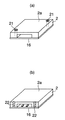
図2(a)には第2実施形態例において特徴的なアンテナモジュールの一例が模式的な斜視図により示され、図2(b)には図2(a)のB−B部分の断面図が模式的に示されている。この第2実施形態例のアンテナモジュール15は、第1実施形態例に示したRF回路一体型アンテナ1が誘電体基体2の底面を接続面として基板16に接合されている形態を有している。なお、この第2実施形態例の説明において、RF回路一体型アンテナ1の構成は第1実施形態例で述べたので、その共通部分の重複説明は省略する。
【0037】
RF回路一体型アンテナ1の底面側には凹部7が形成されており、基板16には、その凹部7によって囲まれる領域に、回路パターン(図示せず)や回路構成部品17が設けられて回路18が形成されている。この回路18は、RF回路一体型アンテナ1のRF回路4に、接続手段である配線パターン10A,10Bなどを介して導通接続される。
【0038】
ところで、電波の送信あるいは受信に関わる回路として、例えば、ベースバンド回路などの信号処理回路や、必要に応じて設けられる周波数変換回路などがある。この第2実施形態例では、それら回路の中から適宜に選択された回路が、回路18として基板16に形成されている。
【0039】
この第2実施形態例によれば、RF回路一体型アンテナ1の誘電体基体2の底面に凹部7を設けたことにより、誘電体基体2の底面側に空間が形成されるので、この空間を有効に利用してアンテナモジュール15を構成した。つまり、RF回路一体型アンテナ1の底面に基板16を接合し、この基板16にはRF回路一体型アンテナ1の底面側の凹部7によって囲まれる領域に回路18を構成した。これにより、簡単な構造で、コンパクトなアンテナモジュールを提供することができる。
【0040】
また、通信機の回路基板において、RF回路一体型アンテナ1を実装する領域に、周波数変換回路や信号処理回路などの回路をも形成されるので、アンテナ実装領域とは別にその回路を形成するための領域を設けなくてよい分、通信機の回路基板の小型化を図ることができて、通信機の小型化を促進させることが可能となる。
【0041】
さらに、RF回路一体型アンテナ1では誘電体基体2の凹部7の内周面のほぼ全面にグランド電極8が形成されており、アンテナ1に収納される回路18はそのグランド電極8によって覆われる構成となっている。このため、そのグランド電極8によって、アンテナ1に収納される回路18はシールドされることとなる。つまり、グランド電極8は、回路18のシールド手段となっている。これにより、そのアンテナ1に収納される回路18は外部からの電磁波の悪影響を受け難く、回路18の動作を安定化させることができる。
【0042】
なお、この発明は上記各実施形態例に限定されるものではなく、様々な実施の形態を採り得る。例えば、誘電体基体2に形成されるRF回路4の回路構成は特に限定されるものではなく、適宜の回路構成を採り得るものである。これにより、例えばRF回路4の回路パターン5は、図1や図2に示される形状に限定されるものではない。例えば、回路パターン5は放射電極3に直接的に導通接続されていてもよい。また、上記各実施形態例では、誘電体基体2にはスイッチ素子である回路構成部品6が設けられていたが、もちろん、スイッチ素子以外の回路構成部品を誘電体基体2に搭載してもよい。このように、誘電体基体2の上面に形成される回路パターンの形状や、回路構成部品の種類や個数は、RF回路4の回路構成に応じて適宜に形成されるものである。
【0043】
また、上記各実施形態例では、誘電体基体2には2個の放射電極3が設けられていたが、放射電極3の配設数は3個以上でもよく、複数であれば、数に限定されるものではない。さらに、上記各実施形態例では、各放射電極3a,3bにそれぞれ一対一に対応するRF回路4a,4bが設けられていたが、例えば、受信用の放射電極3aと、送信用の放射電極3bとに加えて、別の受信用の放射電極が誘電体基体2に形成され、この受信用の放射電極が放射電極3aと共通の受信回路に接続される構成とする場合には、それら受信用の放射電極に共通のRF回路を設けてもよい。このように、各放射電極にそれぞれ一対一に対応させてRF回路を設けなくともよい。
【0044】
さらに、誘電体基体2の形状は特に限定されるものではなく、適宜の形状を採り得る。例えば、図3に示されるように、誘電体基体2の側面に、凹部7に連通接続する開口部20を設けてもよい。また、誘電体基体2を図4(a)に示されるように略円柱状としてもよい。なお、図4(b)には、その円柱状の誘電体基体2を底面側から見た図が示されている。この図に示されるように、誘電体基体2がどのような形状であっても、少なくとも放射電極3が形成される誘電体基体2の部位は肉厚部分となるように、誘電体基体2の底面側に凹部7が形成されることとなる。
【0045】
さらに、上記各実施形態例では、誘電体基体2に形成されているRF回路4を他の回路に接続させるための接続手段として、誘電体基体2の側面に形成されている配線パターン10が設けられていたが、例えば、接続手段としてスルーホールを利用してもよい。また、図5(a)に示されるように、接続手段として、誘電体基体2の上面2aから底面に向けて貫通配置した金属ピン21を設けてもよい。この場合には、接続手段として配線パターンを利用する場合よりも接続の信頼性を高めることができる。さらに、図5(b)に示されるように、接続手段として、スルーホールを用いた側面電極22を設けてもよい。
【0046】
さらに、上記各実施形態例では、誘電体基体2には、受信専用の放射電極と、送信専用の放射電極とが設けられていたが、誘電体基体2に形成されている複数の放射電極の全てが受信専用であってもよいし、また、送信専用であってもよいし、送受信兼用のものであってもよい。さらに、受信専用の放射電極と、送信専用の放射電極と、送受信兼用の放射電極とを適宜に組み合わせてもよい。
【0047】
【発明の効果】
この発明によれば、誘電体基体の略平坦な上面には複数の放射電極が間隔を介して配置されると共に、RF回路が少なくとも一部を前記放射電極間の間隙に配置させて形成されている構成とした。これにより、複数の放射電極は、RF回路が形成される程の間隔を持って離間配置されることとなり、各放射電極のアイソレーションを確保することができる。また、放射電極間の誘電体基体部分を凹部による肉薄部分とすることにより、放射電極間の結合を低減することができる。このことも、各放射電極間のアイソレーションを確保することに大きく関与している。
【0048】
さらに、複数の放射電極が並設される場合に、従来では、それら放射電極間の間隙はデッドスペースであったが、この発明では、その放射電極間の間隙を有効に利用して、RF回路を形成している。このため、RF回路を誘電体基体に設けても、誘電体基体の大型化を抑えることができて、コスト増加を抑制することができる。
【0049】
さらに、アンテナの誘電体基体にRF回路を形成するので、通信機の回路基板にRF回路を設けなくてよく、その分、回路基板を小型化することができて、通信機の小型化を図ることが容易となる。
【0050】
さらに、放射電極と、RF回路とを同一平面上に形成して近接配置したので、放射電極とRF回路間の信号の導通経路が非常に短くなり、導通損失を抑制することができる。
【0051】
さらに、この発明では、放射電極は誘電体基体の肉厚部分に形成されているので、当該放射電極による電波の送信あるいは受信を良好にすることができる。また、RF回路の回路パターンは誘電体基体の肉薄部分に形成されているので、回路パターンの電界が閉じ込められて回路パターンの放射損失を抑えることができる。このような回路パターンの放射損失の抑制効果と、前記導通損失の抑制効果とによって、この発明のアンテナは損失を大幅に低減することができ、これにより、送信あるいは受信の感度を高めることができる。このため、RF回路一体型アンテナや、アンテナモジュールや、通信機の通信の信頼性を向上させることが可能となる。
【0052】
さらに、複数の放射電極が互いに異なる共振周波数を有しているものにあっては、各放射電極のアイソレーションを高めることができる。
【0053】
さらに、この発明のRF回路一体型アンテナを利用したアンテナモジュールにおいては、RF回路一体型アンテナの誘電体基体の凹部により形成された空間を有効に利用し、その空間にRF回路に接続される回路が形成されている。つまり、アンテナの内部に回路が形成された形態となっている。このため、そのアンテナの内部の回路を通信機の回路基板に形成しなくともよくなり、その分、回路基板を小さくすることができて、通信機の小型化をより促進させることができる。
【0054】
RF回路一体型アンテナの誘電体基体の上面に形成されたRF回路と、アンテナの内部に収納された回路とを接続するための手段として、スルーホールを設けたものや、誘電体基体の側面に配線パターンを形成したものにあっては、RF回路一体型アンテナを、回路が形成された基板に接合するだけで、アンテナのRF回路と、基板の回路とを簡単に導通接続させることができて、組み立て効率を良くすることができる。また、接続手段として、金属ピンを用いたものにあっては、RF回路と、基板の回路との接続の信頼性を高めることができる。
【図面の簡単な説明】
【図1】第1実施形態例において特徴的なRF回路一体型アンテナを説明するための図である。
【図2】第2実施形態例において特徴的なアンテナモジュールを説明するための図である。
【図3】その他の実施形態例を説明するための図である。
【図4】さらに、その他の実施形態例を説明するための図である。
【図5】さらにまた、その他の実施形態例を説明するための図である。
【図6】放射電極を誘電体基体の肉厚部分に設けた場合を模式的に示す図である。
【図7】放射電極間の誘電体基体部分を肉薄部分としたことによる効果を説明するための図である。
【符号の説明】
1 RF回路一体型アンテナ
2 誘電体基体
3 放射電極
4 RF回路
5 回路パターン
7 凹部
8 グランド電極
10 配線パターン
21 金属ピン[0001]
BACKGROUND OF THE INVENTION
The present invention relates to an RF circuit-integrated antenna that can be mounted on a circuit board of a communication device, an antenna module including the antenna, and a communication device using the same.
[0002]
[Background]
In recent years, communication devices such as in-vehicle communication devices and portable communication devices have been required to be downsized, and as a result, antennas have also been required to be downsized. For this reason, research and development of surface-mounted antennas, that is, chip-shaped antennas that can be surface-mounted on a circuit board of a communication device, have been actively conducted. The surface-mounted antenna is, for example, one in which a radiation electrode for transmitting or receiving radio waves is formed on a dielectric substrate.
[0003]
[Problems to be solved by the invention]
By the way, for example, there is one in which a plurality of radiation electrodes are formed on a dielectric substrate in order to transmit or receive radio waves in a plurality of frequency bands with one surface mount antenna. In this way, when multiple radiation electrodes are formed on the same dielectric substrate, the dielectric constant of the dielectric substrate that contributes to miniaturization strengthens the coupling between the radiation electrodes, thus ensuring isolation of each radiation electrode. Therefore, it is necessary to widen the interval between the radiation electrodes, and there is a problem that the antenna becomes large. Such an increase in the size of the antenna has caused a problem that the size reduction of the communication device is hindered.
[0004]
The present invention has been made to solve the above-described problems, and an object of the present invention is to provide an RF circuit integrated antenna that can facilitate the miniaturization of a communication device, an antenna module using the same, and an antenna module using the same. To provide a communication device.
[0005]
[Means for Solving the Problems]
In order to achieve the above object, the present invention has the following configuration as means for solving the above problems. That is, the first invention has a dielectric substrate, and the upper surface of the dielectric substrate is substantially flat, and a plurality of radiations for transmitting and / or receiving radio waves are formed on the upper surface of the dielectric substrate. The electrodes are arranged at intervals, and an RF circuit having a circuit pattern and connected to the radiation electrode through a conductive connection or a capacitor is formed by arranging at least a part in the gap between the radiation electrodes. In addition, a concave portion is formed on the bottom surface of the dielectric substrate at a portion corresponding to the circuit pattern formation region of the RF circuit, and a thin portion and a thick portion are formed on the dielectric substrate by the concave portion. The circuit pattern is provided on the thin portion of the dielectric substrate, and the radiation electrode is provided on the thick portion of the dielectric substrate. A ground electrode is formed on the bottom surface of the dielectric substrate and the inner peripheral surface of the recess. It is characterized by To have.
[0006]
The second invention is characterized by comprising the configuration of the first invention, wherein the plurality of radiation electrodes have different resonance frequencies.
[0007]
According to a third aspect of the invention, there is provided the configuration of the first or second aspect, wherein at least one radiation electrode dedicated for reception and one radiation electrode dedicated for transmission are formed on the upper surface of the dielectric substrate. Yes.
[0008]
According to a fourth aspect of the invention, there is provided a configuration according to any one of the first to third aspects of the invention, wherein the RF circuit is formed so as to correspond to each radiation electrode on a one-to-one basis.
[0009]
A fifth invention relates to an antenna module, and the RF circuit integrated antenna according to any one of the first to fourth inventions is joined to a substrate with a bottom surface as a connection surface, and the substrate includes an RF circuit. A circuit that is conductively connected to the RF circuit of the RF circuit-integrated antenna is formed in a region surrounded by the concave portion on the bottom surface side of the circuit-integrated antenna, and connection means for conductively connecting this circuit and the RF circuit is provided. It is characterized by being.
[0010]
According to a sixth aspect of the invention, there is provided the configuration of the fifth aspect of the invention, wherein the connecting means is constituted by a through hole formed in a dielectric substrate of the RF circuit integrated antenna.
[0011]
According to a seventh aspect of the invention, there is provided the configuration of the fifth aspect of the invention, wherein the connecting means is constituted by a wiring pattern formed on the side surface of the dielectric substrate of the RF circuit integrated antenna.
[0012]
According to an eighth aspect of the invention, there is provided the configuration of the fifth aspect of the invention, wherein the connecting means is constituted by a metal pin having a dielectric substrate of an RF circuit integrated antenna penetrating from the top surface to the bottom surface. .
[0013]
A ninth invention relates to a communication device, and the RF circuit integrated antenna according to any one of the first to fourth inventions or the antenna module according to any one of the fifth to eighth inventions. It is characterized by being provided.
[0014]
In the present invention, a plurality of radiation electrodes are disposed on the upper surface of the dielectric substrate with a space therebetween, and an RF circuit is formed with at least a portion disposed in the gap between the radiation electrodes. As described above, since the RF circuit is formed on the dielectric substrate by effectively utilizing the gaps between the plurality of radiation electrodes, only the plurality of radiation electrodes are provided on the dielectric substrate while suppressing an increase in the size of the dielectric substrate. In addition, an RF circuit can be formed.
[0015]
Further, since the RF circuit is formed on the antenna, it is not necessary to form the RF circuit on the circuit board of the communication device, and accordingly, the circuit board can be made smaller, and the communication device can be downsized. be able to.
[0016]
Furthermore, as shown in FIG. 6, by forming the radiation electrode on the thick portion of the dielectric substrate, the radiation electrode can perform a favorable resonance operation and improve the performance of transmission or reception of radio waves. . Further, by forming the circuit pattern in the thin portion of the dielectric substrate, it is possible to suppress radiation loss caused by confining the electric field of the circuit pattern and radiating radio waves from the circuit pattern. In addition, as shown in FIG. 7B, the dielectric substrate portion between the radiation electrodes is recessed as compared with the case where a plurality of radiation electrodes are formed on the dielectric substrate having a uniform thickness as shown in FIG. By reducing the thickness, the coupling between the radiation electrodes can be reduced. Furthermore, another circuit can be accommodated in the recess.
[0017]
DETAILED DESCRIPTION OF THE INVENTION
Embodiments according to the present invention will be described below with reference to the drawings.
[0018]
FIG. 1A schematically shows an RF circuit integrated antenna characteristic of the radio of the first embodiment, and FIG. 1B shows an AA portion shown in FIG. A schematic cross-sectional view is shown. There are various configurations of the radio, and in the first embodiment, any configuration of the radio other than the RF circuit integrated antenna described below may be adopted. Here, the RF circuit is used. A description of the radio unit configuration other than the integrated antenna is omitted.
[0019]
The RF circuit integrated
[0020]
Further, an RF circuit 4 (4a) corresponding to the
[0021]
Further, in the first embodiment,
[0022]
On the
[0023]
A
[0024]
The RF circuit integrated
[0025]
When a transmission signal is supplied from the transmission circuit on the circuit board to the
[0026]
In the example shown in FIG. 1, the
[0027]
According to the first embodiment, a plurality of
[0028]
In addition, since the
[0029]
Furthermore, since the
[0030]
Further, since the
[0031]
In this way, not only the
[0032]
Furthermore, in the first embodiment, the
[0033]
Furthermore, in this first embodiment, the portion of the
[0034]
As described above, since both the conduction loss and the radiation loss of the
[0035]
The second embodiment will be described below. The communication device of the second embodiment is characterized in that an antenna module described below is provided, and any configuration of the communication device other than the antenna module may be adopted. Here, the antenna module is used. Description of the configuration of the other communication devices will be omitted.
[0036]
FIG. 2A is a schematic perspective view showing an example of an antenna module characteristic in the second embodiment, and FIG. 2B is a cross-sectional view taken along the line BB in FIG. Is schematically shown. The
[0037]
A
[0038]
By the way, as a circuit related to transmission or reception of radio waves, for example, there are a signal processing circuit such as a baseband circuit and a frequency conversion circuit provided as necessary. In the second embodiment, a circuit appropriately selected from these circuits is formed on the
[0039]
According to the second embodiment, since the
[0040]
In addition, since a circuit such as a frequency conversion circuit and a signal processing circuit is also formed in a region where the RF circuit integrated
[0041]
Further, in the RF circuit integrated
[0042]
The present invention is not limited to the above embodiments, and various embodiments can be adopted. For example, the circuit configuration of the
[0043]
In each of the above embodiments, the
[0044]
Furthermore, the shape of the
[0045]
Further, in each of the above embodiments, the wiring pattern 10 formed on the side surface of the
[0046]
Further, in each of the above embodiments, the
[0047]
【The invention's effect】
According to the present invention, a plurality of radiating electrodes are arranged on the substantially flat upper surface of the dielectric substrate with a gap therebetween, and an RF circuit is formed by arranging at least a part in the gap between the radiating electrodes. It was set as the composition. Accordingly, the plurality of radiation electrodes are spaced apart from each other so that the RF circuit is formed, and the isolation of each radiation electrode can be ensured. Moreover, the coupling | bonding between radiation electrodes can be reduced by making the dielectric base part between radiation electrodes into the thin part by a recessed part. This also greatly contributes to ensuring isolation between the radiation electrodes.
[0048]
Further, when a plurality of radiation electrodes are arranged in parallel, conventionally, the gap between the radiation electrodes has been a dead space. However, in the present invention, the gap between the radiation electrodes is effectively used to generate an RF circuit. Is forming. For this reason, even if the RF circuit is provided on the dielectric substrate, an increase in the size of the dielectric substrate can be suppressed, and an increase in cost can be suppressed.
[0049]
Further, since the RF circuit is formed on the dielectric base of the antenna, it is not necessary to provide the RF circuit on the circuit board of the communication device, and accordingly, the circuit board can be reduced in size and the communication device can be reduced in size. It becomes easy.
[0050]
Furthermore, since the radiation electrode and the RF circuit are formed on the same plane and arranged close to each other, the signal conduction path between the radiation electrode and the RF circuit becomes very short, and conduction loss can be suppressed.
[0051]
Furthermore, in this invention, since the radiation electrode is formed on the thick portion of the dielectric substrate, it is possible to improve the transmission or reception of radio waves by the radiation electrode. Further, since the circuit pattern of the RF circuit is formed in the thin portion of the dielectric substrate, the electric field of the circuit pattern is confined and the radiation loss of the circuit pattern can be suppressed. Due to the suppression effect of the radiation loss of the circuit pattern and the suppression effect of the conduction loss, the antenna of the present invention can greatly reduce the loss, and thereby the sensitivity of transmission or reception can be increased. . For this reason, it becomes possible to improve the reliability of RF circuit integrated antennas, antenna modules, and communication devices.
[0052]
Furthermore, when the plurality of radiation electrodes have different resonance frequencies, the isolation of each radiation electrode can be increased.
[0053]
Furthermore, in the antenna module using the RF circuit integrated antenna according to the present invention, a circuit formed by effectively using the space formed by the concave portion of the dielectric substrate of the RF circuit integrated antenna and connected to the RF circuit in the space. Is formed. That is, a circuit is formed inside the antenna. For this reason, it is not necessary to form the circuit inside the antenna on the circuit board of the communication device, and the circuit board can be made smaller by that amount, and the size reduction of the communication device can be further promoted.
[0054]
As a means for connecting the RF circuit formed on the upper surface of the dielectric substrate of the RF circuit-integrated antenna and the circuit accommodated in the antenna, a device provided with a through hole or a side surface of the dielectric substrate. In the case where the wiring pattern is formed, the RF circuit of the antenna and the circuit of the substrate can be easily conductively connected simply by joining the RF circuit integrated antenna to the substrate on which the circuit is formed. Assembling efficiency can be improved. Further, in the case where a metal pin is used as the connection means, the reliability of connection between the RF circuit and the circuit on the substrate can be improved.
[Brief description of the drawings]
FIG. 1 is a diagram for explaining a characteristic RF circuit-integrated antenna in a first embodiment.
FIG. 2 is a diagram for explaining a characteristic antenna module in a second embodiment.
FIG. 3 is a diagram for explaining another embodiment.
FIG. 4 is a diagram for explaining another embodiment.
FIG. 5 is a diagram for explaining still another embodiment.
FIG. 6 is a diagram schematically showing a case where a radiation electrode is provided on a thick portion of a dielectric substrate.
FIG. 7 is a diagram for explaining an effect obtained by making a dielectric base portion between radiation electrodes thin.
[Explanation of symbols]
1 RF circuit integrated
Claims (9)
Priority Applications (4)
| Application Number | Priority Date | Filing Date | Title |
|---|---|---|---|
| JP2001239303A JP3649168B2 (en) | 2001-08-07 | 2001-08-07 | RF circuit integrated antenna, antenna module using the same, and communication device including the same |
| US10/189,424 US6646609B2 (en) | 2001-08-07 | 2002-07-08 | Antenna with an integral RF circuit, antenna module incorporating the same, and communication apparatus incorporating the same |
| DE60203150T DE60203150T2 (en) | 2001-08-07 | 2002-08-07 | Antenna with an integrated RF circuit, antenna module and communication device with such elements |
| EP02017815A EP1289052B1 (en) | 2001-08-07 | 2002-08-07 | Antenna with an integral RF circuit, antenna module and communication apparatus incorporating the same |
Applications Claiming Priority (1)
| Application Number | Priority Date | Filing Date | Title |
|---|---|---|---|
| JP2001239303A JP3649168B2 (en) | 2001-08-07 | 2001-08-07 | RF circuit integrated antenna, antenna module using the same, and communication device including the same |
Publications (2)
| Publication Number | Publication Date |
|---|---|
| JP2003051711A JP2003051711A (en) | 2003-02-21 |
| JP3649168B2 true JP3649168B2 (en) | 2005-05-18 |
Family
ID=19070075
Family Applications (1)
| Application Number | Title | Priority Date | Filing Date |
|---|---|---|---|
| JP2001239303A Expired - Fee Related JP3649168B2 (en) | 2001-08-07 | 2001-08-07 | RF circuit integrated antenna, antenna module using the same, and communication device including the same |
Country Status (4)
| Country | Link |
|---|---|
| US (1) | US6646609B2 (en) |
| EP (1) | EP1289052B1 (en) |
| JP (1) | JP3649168B2 (en) |
| DE (1) | DE60203150T2 (en) |
Cited By (1)
| Publication number | Priority date | Publication date | Assignee | Title |
|---|---|---|---|---|
| WO2007049376A1 (en) * | 2005-10-27 | 2007-05-03 | Murata Manufacturing Co., Ltd. | High-frequency module |
Families Citing this family (27)
| Publication number | Priority date | Publication date | Assignee | Title |
|---|---|---|---|---|
| DE10113349A1 (en) * | 2001-03-20 | 2002-09-26 | Philips Corp Intellectual Pty | Antenna with substrate and conducting track has at least one aperture formed by hollow chamber enclosed by substrate or by recess formed in one or more surfaces of substrate |
| AU2002340506A1 (en) * | 2002-11-07 | 2004-06-07 | Fractus, S.A. | Integrated circuit package including miniature antenna |
| JP2004274418A (en) * | 2003-03-10 | 2004-09-30 | Tdk Corp | Antenna integrated module |
| DE10350034A1 (en) | 2003-10-27 | 2005-05-25 | Robert Bosch Gmbh | Antenna arrangement in particular for radar applications in motor vehicles |
| EP1771919A1 (en) * | 2004-07-23 | 2007-04-11 | Fractus, S.A. | Antenna in package with reduced electromagnetic interaction with on chip elements |
| EP1810369A1 (en) * | 2004-09-27 | 2007-07-25 | Fractus, S.A. | Tunable antenna |
| US7683839B2 (en) * | 2006-06-30 | 2010-03-23 | Nokia Corporation | Multiband antenna arrangement |
| CN101227202B (en) * | 2007-01-19 | 2011-07-27 | 鸿富锦精密工业(深圳)有限公司 | Electronic device |
| US7760142B2 (en) * | 2007-04-10 | 2010-07-20 | Emag Technologies, Inc. | Vertically integrated transceiver array |
| US8878727B2 (en) * | 2009-02-12 | 2014-11-04 | Origin Gps Ltd. | Antenna-module hybrid circuit |
| JP2012253436A (en) * | 2011-05-31 | 2012-12-20 | Tdk Corp | Triple band antenna device and radio communication apparatus using the same |
| JP6168394B2 (en) * | 2013-05-02 | 2017-07-26 | 三菱マテリアル株式会社 | Antenna device |
| USD757693S1 (en) * | 2013-09-26 | 2016-05-31 | Murata Manufacturing Co., Ltd. | Wireless transmission/reception module |
| USD892774S1 (en) * | 2013-09-26 | 2020-08-11 | Murata Manufacturing Co., Ltd. | Wireless transmission/reception module |
| JP6238239B2 (en) * | 2014-11-27 | 2017-11-29 | アルプス電気株式会社 | Communication module |
| WO2016120254A1 (en) * | 2015-01-27 | 2016-08-04 | At & S Austria Technologie & Systemtechnik Aktiengesellschaft | Component carrier with integrated antenna structure |
| USD768115S1 (en) * | 2015-02-05 | 2016-10-04 | Armen E. Kazanchian | Module |
| US10971806B2 (en) | 2017-08-22 | 2021-04-06 | The Boeing Company | Broadband conformal antenna |
| US11233310B2 (en) * | 2018-01-29 | 2022-01-25 | The Boeing Company | Low-profile conformal antenna |
| JP2019176202A (en) * | 2018-03-26 | 2019-10-10 | 富士通コンポーネント株式会社 | Wireless module |
| KR20200140310A (en) | 2018-04-03 | 2020-12-15 | 코닝 인코포레이티드 | Electronic package including structured glass article and method for manufacturing same |
| US10916853B2 (en) | 2018-08-24 | 2021-02-09 | The Boeing Company | Conformal antenna with enhanced circular polarization |
| US10938082B2 (en) | 2018-08-24 | 2021-03-02 | The Boeing Company | Aperture-coupled microstrip-to-waveguide transitions |
| US10923831B2 (en) | 2018-08-24 | 2021-02-16 | The Boeing Company | Waveguide-fed planar antenna array with enhanced circular polarization |
| WO2021000071A1 (en) * | 2019-06-29 | 2021-01-07 | 瑞声声学科技(深圳)有限公司 | Antenna module and mobile terminal |
| US11276933B2 (en) | 2019-11-06 | 2022-03-15 | The Boeing Company | High-gain antenna with cavity between feed line and ground plane |
| WO2022230427A1 (en) * | 2021-04-28 | 2022-11-03 | 株式会社村田製作所 | Antenna device |
Family Cites Families (6)
| Publication number | Priority date | Publication date | Assignee | Title |
|---|---|---|---|---|
| JPH114113A (en) * | 1997-04-18 | 1999-01-06 | Murata Mfg Co Ltd | Surface mount antenna and communication apparatus using the same |
| JPH1168456A (en) * | 1997-08-19 | 1999-03-09 | Murata Mfg Co Ltd | Surface mounting antenna |
| WO2000048269A1 (en) * | 1999-02-15 | 2000-08-17 | Communications Research Laboratory, Independent Administrative Institution | Radio communication device |
| JP2000278009A (en) * | 1999-03-24 | 2000-10-06 | Nec Corp | Microwave/millimeter wave circuit device |
| TW431033B (en) * | 1999-09-03 | 2001-04-21 | Ind Tech Res Inst | Twin-notch loaded type microstrip antenna |
| CA2426497C (en) * | 1999-09-09 | 2005-06-28 | Murata Manufacturing Co., Ltd. | Surface-mount antenna and communication device with surface-mount antenna |
-
2001
- 2001-08-07 JP JP2001239303A patent/JP3649168B2/en not_active Expired - Fee Related
-
2002
- 2002-07-08 US US10/189,424 patent/US6646609B2/en not_active Expired - Fee Related
- 2002-08-07 EP EP02017815A patent/EP1289052B1/en not_active Expired - Lifetime
- 2002-08-07 DE DE60203150T patent/DE60203150T2/en not_active Expired - Lifetime
Cited By (3)
| Publication number | Priority date | Publication date | Assignee | Title |
|---|---|---|---|---|
| WO2007049376A1 (en) * | 2005-10-27 | 2007-05-03 | Murata Manufacturing Co., Ltd. | High-frequency module |
| JPWO2007049376A1 (en) * | 2005-10-27 | 2009-04-30 | 株式会社村田製作所 | High frequency module |
| JP4725582B2 (en) * | 2005-10-27 | 2011-07-13 | 株式会社村田製作所 | High frequency module |
Also Published As
| Publication number | Publication date |
|---|---|
| DE60203150T2 (en) | 2006-05-11 |
| EP1289052B1 (en) | 2005-03-09 |
| DE60203150D1 (en) | 2005-04-14 |
| EP1289052A3 (en) | 2004-01-14 |
| US20030030587A1 (en) | 2003-02-13 |
| EP1289052A2 (en) | 2003-03-05 |
| US6646609B2 (en) | 2003-11-11 |
| JP2003051711A (en) | 2003-02-21 |
Similar Documents
| Publication | Publication Date | Title |
|---|---|---|
| JP3649168B2 (en) | RF circuit integrated antenna, antenna module using the same, and communication device including the same | |
| EP1368858B1 (en) | Module and electronic device | |
| US6535167B2 (en) | Laminate pattern antenna and wireless communication device equipped therewith | |
| JP3734807B2 (en) | Electronic component module | |
| JP3868775B2 (en) | ANTENNA DEVICE AND COMMUNICATION DEVICE USING THE SAME | |
| JP2004201278A (en) | Pattern antenna | |
| JP2004327641A (en) | Electronic component module | |
| JP2002076735A (en) | Pattern antenna and radio communication equipment using the same | |
| KR20030078926A (en) | Antenna incorporating filter | |
| JP2014112645A (en) | High-frequency circuit module | |
| JP2001358517A (en) | Antenna device and radio equipment using the same | |
| US7109948B2 (en) | Dielectric antenna module | |
| JP2004096206A (en) | Waveguide / planar line converter, and high frequency circuit apparatus | |
| JP2002353842A (en) | Wireless module for mobile terminal | |
| JP4479606B2 (en) | Antenna device | |
| JPH08111609A (en) | Antenna system | |
| CN116057842A (en) | High-frequency module and communication device | |
| JP2007036315A (en) | High frequency electric component | |
| JP2002280809A (en) | United structure of high frequency component and high frequency transmission line conversion circuit | |
| JP2003309423A (en) | Antenna integrated high frequency circuit module | |
| JP3700377B2 (en) | Surface mount antenna and communication device equipped with the same | |
| JP2003124830A (en) | Composite antenna | |
| JP3995206B2 (en) | Module with antenna | |
| CN114696069B (en) | Electronic equipment | |
| JP3932920B2 (en) | Antenna integrated high-frequency circuit module |
Legal Events
| Date | Code | Title | Description |
|---|---|---|---|
| A977 | Report on retrieval |
Free format text: JAPANESE INTERMEDIATE CODE: A971007 Effective date: 20050112 |
|
| TRDD | Decision of grant or rejection written | ||
| A01 | Written decision to grant a patent or to grant a registration (utility model) |
Free format text: JAPANESE INTERMEDIATE CODE: A01 Effective date: 20050125 |
|
| A61 | First payment of annual fees (during grant procedure) |
Free format text: JAPANESE INTERMEDIATE CODE: A61 Effective date: 20050207 |
|
| R150 | Certificate of patent or registration of utility model |
Free format text: JAPANESE INTERMEDIATE CODE: R150 |
|
| FPAY | Renewal fee payment (event date is renewal date of database) |
Free format text: PAYMENT UNTIL: 20090225 Year of fee payment: 4 |
|
| FPAY | Renewal fee payment (event date is renewal date of database) |
Free format text: PAYMENT UNTIL: 20090225 Year of fee payment: 4 |
|
| FPAY | Renewal fee payment (event date is renewal date of database) |
Free format text: PAYMENT UNTIL: 20100225 Year of fee payment: 5 |
|
| FPAY | Renewal fee payment (event date is renewal date of database) |
Free format text: PAYMENT UNTIL: 20110225 Year of fee payment: 6 |
|
| LAPS | Cancellation because of no payment of annual fees |