BACKGROUND OF THE INVENTION
Field of the Invention
The present invention relates to a tablet for producing a one-sided sealing-type
semiconductor device, comprising an epoxy resin composition with
suppression in the generation of bowing and high reliability, a wafer with a resin
layer and a semiconductor device produced by using the tablet.
Discussion of the Related Art
Conventionally, a cured resin layer is formed on one side of a wafer
comprising a plural projected electrodes by subjecting a tablet comprising an
epoxy resin composition to hot press molding, wherein the epoxy resin
composition is obtained by cold pressing molding. However, in the wafer with a
resin layer in which a cured resin layer is formed by using the tablet described
above, there arises a problem that bowing is generated. Specifically, when a
cured resin layer is formed by using the above-mentioned tablet, the bowing of
the wafer with a resin layer is undesirably caused because the physical properties
such as a coefficient of linear expansion of a cured product of an epoxy resin
composition, which is the cured resin layer, are different from those of a wafer.
The wafer with a resin layer in which the bowing described above is generated
causes troubles during conveying and dicing, and has a defect that its
applicability to the substrate becomes poor. Further, there also arise some
problems that a stress is generated at the interface of the wafer and the cured
resin layer, so that its reliability is impaired.
In addition, in the technique of packaging (sealing) a semiconductor
element in the field of semiconductor devices in the recent years, one-sided
sealing-type semiconductor devices, for instance, have been remarked and
actually used. A semiconductor device in which a semiconductor element is
sealed by a cured product of an epoxy resin composition has excellent
mass-producibility and low costs. Further, the above-mentioned one-sided
sealing type semiconductor device can have high performance by highly
integrating the semiconductor element. In addition, in a method of mounting a
semiconductor element to a board, which is the insulating substrate mentioned
above in a flip chip manner or a direct chip attachment manner, sealing is usually
carried out by one-sided sealing in a state of incorporating the semiconductor
element, or alternatively by filling a molten thermosetting resin composition in a
void between the insulating substrate and the semiconductor device and curing
the composition. However, these semiconductor devices have some problems of
generation of bowing of the package caused by curing shrinkage of a sealing
resin, and incongruence in the coefficients of linear expansion of the insulating
substrate and the sealing resin (cured product). In the semiconductor device in
which the bowing described above is generated, pealing or the like is caused at
the sealing interface by the stress due to bowing, so that its reliability is lowered,
thereby resulting in poor applicability to a substrate. Therefore, a solution to
such a problem is desired.
An object of the present invention to provide a tablet comprising an epoxy
resin composition for producing a one-sided sealing-type semiconductor device
with suppression in the generation of bowing and high reliability.
Another object of the present invention is to provide a wafer and a
semiconductor device produced by using a tablet comprising an epoxy resin
composition, and processes for producing the tablet and the wafer.
Still another object of the present invention is to provide a method of
preventing generation of bowing of the wafer and the semiconductor device.
Still another object of the present invention is to provide a use of a tablet
comprising an epoxy resin composition for preventing generation of bowing of
the wafer and the semiconductor device.
These and other objects of the present invention will be apparent from the
following description.
SUMMARY OF THE INVENTION
The present inventors have again studied on causation of bowing of the
wafer with a resin layer from various angles. As a result, they have found that an
amount reduced by heating of the tablet before molding is one of causations of
bowing as well as conventionally known causations of curing shrinkage of the
cured resin layer and incongruence in coefficients of linear expansion of the
wafer and the cured resin layer. It is thought that the shrinkage of the resin is
caused by exhalation of volatile components remaining in the internal of the
cured resin layer when pressure-releasing.
The same can be said for the causations of bowing of the package. As a
result of further studies based on these findings, in order to suppress the
generation of the above-mentioned bowing, the present inventors have found that
it is effective to reduce volatile components in the tablet usable for formation of
the cured resin layer of a wafer with a resin layer, or the volatile components in
the tablet before curing usable for sealing a semiconductor element on the
insulating substrate, and to diminish the amount reduced by heating the tablet.
Therefore, the present inventors have found that by using a tablet having an
amount reduced by heating lower than a specified amount of the volatile
components, the shrinkage of the resin due to exhalation when pressure-releasing
can be suppressed, whereby the generation of bowing can be consequently
suppressed. Also, the semiconductor device obtained by using the above-mentioned
tablet of course has high reliability with suppression in the generation
of bowing.
In addition, the present inventors have found that by using as the tablet
one obtained by preparing a molten product comprising an epoxy resin
composition and cooling and solidifying the molten product, the compression
ratio of the tablet is made large and the resin of the tablet is made very dense, so
that the tablet is less likely to be hygroscopic, whereby a tablet having a small
amount reduced by heating can be obtained. Therefore, they have found that
when a tablet of which compression ratio is very high and cured product has a
glass transition temperature of not less than a particular value is used, a
semiconductor device with more effective suppression of the generation of
bowing and high reliability can be obtained. Further, they have found that a
semiconductor device having high reliability can be obtained because the voids
in the molded product can be reduced by having a low volatile component
content and a high compression ratio. The present invention has been
accomplished based on these findings.
Concretely, the present invention pertains to the following:
(A): an amount reduced by heating being less than 0.05% by weight; (2) the tablet according to item (1) above, obtainable by a process comprising
preparing a molten product of the epoxy resin composition in an uncured state,
and thereafter cooling and solidifying the molten product; (3) the tablet according to item (1) or (2) above, further having at least one
characteristic selected from the group consisting of:
(B): a compression ratio of the tablet being 98% or more; and (C): a glass transition temperature of a cured product of the tablet being 120°C
or more; (4) a wafer with a resin layer comprising a plural projected electrodes and a
cured resin layer formed on a projected electrode-mounting side of the wafer,
wherein the cured resin layer is formed by the tablet of any one of items (1) to
(3) above; (5) a semiconductor device obtainable by a process comprising dicing the
wafer with a resin layer of item (4) above into a given size; (6) a semiconductor device comprising an insulating substrate, a
semiconductor element mounted on one side of the insulating substrate, and a
cured product of an epoxy resin composition, the semiconductor element being
incorporated in and sealed by the cured product, wherein the cured product of an
epoxy resin composition is formed by the tablet of any one of items (1) to (3)
above; (7) a semiconductor device comprising an insulating substrate, a
semiconductor element mounted on one side of the insulating substrate via a
plural connecting electrodes, and a cured resin layer sealing a void between the
insulating substrate and the semiconductor element, wherein the cured resin layer
is formed by the tablet of any one of items (1) to (3) above; (8) a process for producing a wafer with a resin layer comprising a plural
projected electrodes and a cured resin layer formed on a projected electrode-mounting
side of the wafer, comprising the steps of putting the tablet of any one
of items (1) to (3) above on the projected electrode-mounting side of the wafer,
and heating the tablet to be melt-cured, thereby forming the cured resin layer; (9) a process for producing a semiconductor device comprising an insulating
substrate, a semiconductor element mounted on one side of the insulating
substrate, and a cured product of an epoxy resin composition, the semiconductor
element being incorporated in and sealed by the cured product, comprising the
steps of putting the tablet of any one of items (1) to (3) above on the
semiconductor element, and heating the tablet to be melt-cured, thereby forming
the cured product; (10) a process for producing a semiconductor device comprising an insulating
substrate, a semiconductor element mounted on one side of the insulating
substrate via a plural connecting electrodes, and a cured resin layer sealing a void
between the insulating substrate and the semiconductor element, comprising the
steps of heat-melting the tablet of any one of items (1) to (3) above, and filling
the void and curing the tablet, thereby forming the cured resin layer; (11) a method for preventing generation of bowing of a wafer, comprising
forming a cured resin layer on a wafer by using the tablet of any one of items (1)
to (3) above; (12) a method for preventing generation of bowing of a semiconductor device,
comprising sealing semiconductor elements on one side of an insulating substrate
by using the tablet of any one of items (1) to (3) above; (13) use of a tablet of any one of items (1) to (3) above for preventing
generation of bowing of a wafer in the production of the wafer in which a cured
resin layer is formed on the wafer; and (14) use of a tablet of any one of items (1) to (3) above for preventing
generation of bowing of a semiconductor device in the production of the
semiconductor device in which semiconductor elements are sealed on one side of
an insulating substrate.
BRIEF DESCRIPTION OF THE DRAWINGS
Figure 1 is an explanatory view showing one example of a production
apparatus for producing a tablet comprising an epoxy resin composition;
Figure 2 is a cross-sectional view showing one example of a wafer with a
resin layer;
Figure 3 is a cross-sectional view showing another example of a wafer
with a resin layer;
Figure 4 is a perspective view of one example of a semiconductor device;
Figure 5 is a cross-sectional view showing a state in which a
semiconductor device is mounted on a printed circuit substrate;
Figure 6 is a cross-sectional view showing one example of a one-sided
sealing-type semiconductor device;
Figure 7 is a cross-sectional view showing one example of a
semiconductor device having a face down structure;
Figure 8 is a cross-sectional view showing a production process of a
semiconductor device having a face down structure;
Figure 9 is a cross-sectional view showing another example of a
semiconductor device having a face down structure;
Figure 10 is a cross-sectional view showing still another example of a
semiconductor device having a face down structure;
Figure 11 is a cross-sectional view showing a state in which bowing of a
wafer with a resin layer is determined;
Figure 12 is a cross-sectional view showing a state in which bowing of a
wafer with a resin layer is determined; and
Figure 13 is a cross-sectional view showing a state in which bowing of a
wafer with a resin layer is determined.
DETAILED DESCRIPTION OF THE INVENTION
The tablet comprising an epoxy resin composition [hereinafter simply
referred to as "tablet"] of the present invention has the following characteristic
(A):
(A): an amount reduced by heating being less than 0.05% by weight.
The epoxy resin composition usable for the preparation of the tablet comprises
an epoxy resin and a curing agent.
The above-mentioned epoxy resin is not particularly limited, and
conventionally known various epoxy resins, for instance, cresol novolak epoxy
resins, phenol novolak epoxy resins, bisphenol A epoxy resins, naphthalene
epoxy resins, biphenyl epoxy resins, and the like can be used. Among the
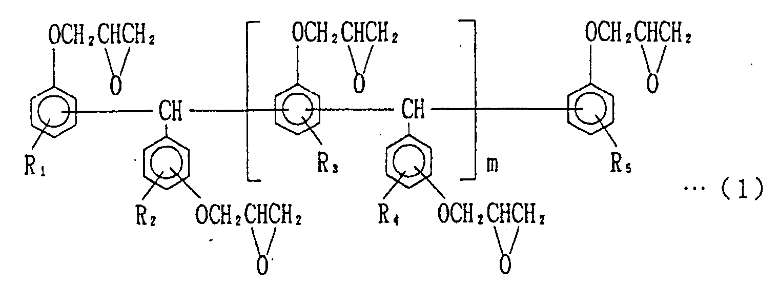
various epoxy resins, it is preferable that the epoxy resin represented by the
following general formula (1):
wherein each of R
1 to R
5, which may be identical or different, is hydrogen atom
or an alkyl group having 1 to 5 carbon atoms; and m is 0 or a positive number of
5 or less,
is used as all or a part of the epoxy resin component, from the viewpoint of
reducing the bowing by improvement in the glass transition temperature.
A preferable curing agent which is usable together with the above-mentioned
epoxy resin includes a phenolic resin. The curing agent is not
particularly limited thereto, and any of conventionally known ones can be used.
The curing agent includes, for instance, phenol novolak, cresol novolak,
bisphenol A novolak, naphthol novolak, triphenylmethane type phenolic resins,
phenol aralkyl resins, and the like.
It is preferable that the formulation ratio of the above-mentioned epoxy
resin to the above-mentioned phenolic resin is adjusted such that hydroxyl
groups in the phenolic resin is from 0.7 to 1.3 equivalents, and especially from
0.9 to 1.1 equivalents per one equivalent of the epoxy group in the above-mentioned
epoxy resin.
It is preferable to further use an inorganic filler together with the above-mentioned
epoxy resin and the phenolic resin. The inorganic filler includes
those in pulverized, ground, or spherical forms, and conventionally known
various fillers can be used without particular limitation. The inorganic filler
includes, for instance, silica powders such as silica glass powder, talc, fused
silica powder and crystalline silica powder; alumina; silicon nitride; aluminum
nitride; silicon carbide; and the like. These inorganic fillers can be used alone or
in admixture of two or more kinds. It is preferable to use the fused silica powder,
from the viewpoint of fluidity, especially spherical fused silica powder. As the
above-mentioned inorganic filler, it is preferable that the average particle size is
in the range of from 0.1 to 50 µm as determined by laser particle size analyzer,
more preferably from 0.1 to 30 µm, still more preferably 0.5 to 10 µm.
It is preferable that the content of the above-mentioned inorganic filler is
adjusted to make up 60 to 95% by weight of the epoxy resin composition.
In the above-mentioned epoxy resin composition, besides the
above-mentioned epoxy resin, the phenolic resin and the inorganic filler, there
can be optionally properly added a curing accelerator, a pigment, a mold-releasing
agent, a flexibility imparting agent, a coupling agent such as a silane
coupling agent such as silane coupling agents containing epoxy group, amino
group, mercapto group, vinyl group or methacryl group, such as
γ-glycidoxypropyl trimethoxysilane; an ion trapping agent, a flame retarder, a
tackifying agent, and the like.
The above-mentioned curing accelerator is not particularly limited, as
long as the curing accelerator acts to accelerate the reaction between epoxy
group and hydroxyl group. The curing accelerator includes, for instance,
diazabicycloalkene compounds such as 1,8-diazabicyclo[5.4.0]undecene-7,1,5-diazabicyclo[4.3.0]nonene-5;
tertiary amines such as triethylenediamine;
imidazoles such as 2-methylimidazole; phosphorus-containing compounds such
as triphenylphosphine; and the like. These compounds can be used alone or in
admixture of two or more compounds.
The above-mentioned pigment includes carbon blacks, titanium oxide,
and the like. Also, the above-mentioned mold-releasing agent includes carnauba
wax, polyethylene waxes, paraffins, esters of fatty acids, salts of fatty acids, and
the like.
The above-mentioned flexibility imparting agent includes various silicone
compounds, acrylonitrile-butadiene rubber, and the like.
The above-mentioned ion trapping agent includes bismuth hydroxide,
hydrotalcite compounds, and the like.
The above-mentioned flame retarder includes brominated novolak epoxy
resins, brominated bisphenol A epoxy resins, metal compounds such as antimony
trioxide, antimony pentoxide, metal hydroxides such as magnesium hydroxide
and aluminum hydroxide, red phosphorus, phosphorus-containing compounds
such as phosphates, and the like. These flame retarders can be used alone or in
admixture of two or more kinds.
Further, as a flame retarder other than the flame retarders mentioned
above, there can be used composite metal hydroxide having a polyhedral shape
represented by the general formula (2):
M1-XQX(OH)2
wherein M is at least one metal atom selected from the group consisting of Mg,
Ca, Sn and Ti; Q is at least one metal atom selected from the group consisting of
Mn, Fe, Co, Ni, Cu and Zn; and X is a positive number of 0.01 to 0.5.
This composite metal hydroxide has the crystalline structure of a polyhedral
form. It does not have a conventional hexahedral form, or a platy form having
thin thickness such as scaly form for the crystalline structure. Rather, it refers to
a composite metal hydroxide having large crystal growth in the direction of
thickness (c-axis direction) as well as in the length and width directions,
including, for instance, those having a granular crystalline form which are made
to resemble steric and spherical form by the crystal growth of a platy crystal in
the direction of thickness (c-axis direction), the granular crystalline forms
including, approximate dodecahedron, approximate octahedron, approximate
tetrahedron, and the like.
For instance, the composite metal hydroxide having large crystal growth
in the direction of thickness (c-axis direction) as well as in the length and width
directions, and a desired polyhedral crystalline form, can be obtained by
controlling various conditions in the manufacturing process of the composite
metal hydroxide, and may be usually a mixture of various shapes.
Concrete representative examples of the composite metal hydroxide
include a hydrate of magnesium oxide and nickel oxide, a hydrate of magnesium
oxide and zinc oxide, a hydrate of magnesium oxide and copper oxide, and the
like.
In addition, the composite metal hydroxide having a polyhedral form has
an aspect ratio of usually from 1 to 8, preferably from 1 to 7, especially
preferably from 1 to 4. The aspect ratio referred to herein is expressed by a ratio
of length to width of the composite metal hydroxide. In other words, in a case
where the aspect ratio exceeds 8, the effect on a decrease in viscosity becomes
poor when an epoxy resin composition comprising the composite metal
hydroxide is melted.
The tablet made from the above materials can be prepared, for instance, as
follows. In other words, the above-mentioned epoxy resin composition is
dry-blended with a mixer, for instance, a Henschel mixer, and the resulting
mixture is melt-kneaded with a kneading extruder. Thereafter, the molten
product is filled into a tablet mold, and the filled material is pressed with cooling
the above-mentioned mold by allowing water to flow through the mold. After
termination of cooling, the formed tablet is taken out from the mold to give a
tablet.
In the above-mentioned preparation steps, it is preferable that the melt-kneading
temperature is adjusted to 60° to 150°C, that a molten resin
temperature during filling is adjusted to 80° to 120°C, and that a mold
temperature is adjusted to 5° to 50°C, respectively.
In the pressure-molding of the molten resin within the above-mentioned
mold, a preferable method comprises arranging the upper and lower plungers in
the tablet mold so that the mold can be closed with the motion of the plungers,
and molding a molten resin composition fed to the tablet mold by the operation
of the plungers, with pressing at a pressure of 490 × 104 to 2940 × 104 Pa or so.
Further, the production process of the tablet will be explained more
concretely hereinbelow. Figure 1 is a view showing one example of a production
apparatus for producing a tablet. 11 Is a kneading extruder, which comprises a
cylinder 12 in which a screw (not illustrated in the figure) is installed. 13 Is a
mold holder which moves in left and right directions along a tracking rail 14, and
is equipped with a cooling jacket. Also, 16 is a tablet mold, which is closed by
an upper plunger 17 and a lower plunger 18. 19 Is a resin feed pipe attached at
tip end of the cylinder 12 of the kneading extruder 11, in which a stirrer is
installed, and a discharge outlet 20 is slidably contacted to an upper face of the
mold. In Figure 1, 21 is a tablet delivery mechanism.
In order to produce a tablet by using the production apparatus described
above, first, a mixture is prepared by mixing each of the above-mentioned
components with a Henschel mixer. Next, this mixture is delivered into a hopper
(not illustrated in the figure) of a kneading extruder 11, and the resin
composition in the above hopper is delivered into a cylinder 12 of the kneading
extruder 11 by rotation of a screw installed in the cylinder 12. The resin
composition is kneaded with heat melting at a temperature of from 60° to 150°C,
and the molten epoxy resin composition is filled in a tablet mold 16 via a resin
feed pipe 19 by an extrusion force of the screw. Thereafter, after the filling of
the molten epoxy resin composition in the tablet mold 16 is completed, a mold
holder 13 moves right (or left). When the left (or left) tablet mold 16 reaches the
position of a discharge outlet 20 of the resin feed pipe 19, the mold holder 13 is
stopped. The molten epoxy resin composition filled in the tablet mold 16 moved
right (or left) is molded with pressing with an upper plunger 17 and a lower
plunger 18 at a pressure of 490 × 104 to 2940 × 104 Pa or so. Cooled water of
which temperature is adjusted to 5° to 50°C is circulated through the cooling
jacket of the mold holder 13.
Next, the cooled resin (25° to 60°C or so) is ejected upwardly by the
lower plunger 18, and the ejected resin, i.e. the tablet, was discharged in a
forward direction by a tablet delivery mechanism 21. Thereafter, on completion
of filling of the resin in the left (or right) mold, the mold moves right (or left),
and the above-operation is repeated, whereby tablets can be produced in a
continuous manner.
The tablet produced as described above is required to have the following
characteristic (A):
(A): an amount reduced by heating being less than 0.05% by weight.
The amount reduced by heating is preferably 0.04% by weight or less,
more preferably 0.03% by weight or less.
Further, it is more preferable that the tablet has at least one characteristic
selected from the group consisting of:
In the above-mentioned characteristics (A) and (B), the more the amount
reduced by heating [characteristic (A)] approximates 0% by weight, the more
preferable, and the more the compression ratio of the tablet [characteristic (B)]
approximates 100%, the more preferable.
The amount reduced by heating in the above-mentioned characteristic (A)
is obtained as follows. Specifically, the obtained tablet is heated at 175°C for
1 hour, and the weights before and after heating are determined, and the amount
reduced by heating is calculated as follows:
Amount Reduced by Heating (% by weight) = (Initial Weight) - (Weight after Heating) (Initial Weight) × 100
The compression ratio in the characteristic (B) of the tablet is obtained as
follows. Specifically, the compression ratio of the above-mentioned tablet is a
ratio of an apparent specific gravity of the tablet and a specific gravity where
voids inside the tablet are zeroed (true specific gravity). For instance, when a
specific gravity of the resin cured product of the tablet is denoted by p, a volume
of the tablet is denoted by V, and a weight of the tablet is denoted by W, the
compression ratio of the tablet can be calculated by the following equation:
The above-mentioned resin cured product of the tablet can be obtained by curing
the resin composition with a transfer molding machine at 175°C for 10 minutes
under a pressure of 1960 × 10
4 Pa or so.
The glass transition temperature in the above-mentioned characteristic (C)
of the cured product is obtained as follows. Specifically, the above-mentioned
tablet is cured by a transfer molding machine at 175°C for 10 minutes, to give a
resin cured product (size: 4 mm × 3 mm × thickness 20 mm). The resin cured
product is cured at 175°C for 5 hours, and then dried at 95°C for 24 hours.
Thereafter, the elongation of the above-mentioned cured product of the epoxy
resin composition is determined by using a thermomechanical analyzer (TMA
device commercially available from Rigaku, model number MJ-800GM) in a
temperature range of 30° to 250°C, and a glass transition temperature can be
obtained from this determination. The determination condition is a heating rate
of 5°C/minute.
A first embodiment of the present invention pertains to a wafer with a
resin layer produced by using a tablet. As shown in Figure 2, the wafer with a
resin layer 1 of the present invention comprises a plural projected electrodes 2
and a cured resin layer 3 formed on a projected electrode-mounting side of the
wafer 1. In the present invention, a wafer refers to a thin plate semiconductor in
which an electrode layer as well as the above-mentioned projected electrodes 2 is
mounted on the surface thereof.
Figure 3 is another example of the wafer with a resin layer of the present
invention. Specifically, a wafer with a resin layer is formed such that a surface
of a cured resin layer formed on a wafer 1 shares the same plane with a tip end of
the projected electrodes 2'.
The material for the above-mentioned plural projected electrodes 2 is not
particularly limited. The material includes, for instance, gold, silver, copper,
aluminum, nickel, chromium, tin, lead, solder, and alloys thereof. In addition,
the shape of the above-mentioned plural projected electrodes 2 is not particularly
limited. It is preferable that the surface of the electrodes has projected shape.
The material for the above-mentioned wafer 1 is not particularly limited,
and there are included any of ones conventionally used, for instance, GaAs wafer,
Si wafer, and the like.
The above-mentioned cured resin layer 3 is formed by using the tablet of
the present invention, and the feature of the present invention resides in that a
semiconductor element is sealed by using the tablet as described above.
The resin with a wafer of the present invention can be prepared by using
the above-mentioned tablet, heat-melting the tablet by means of transfer molding,
compression forming, or the like to form a resin layer on a wafer, and curing the
resin layer. In other words, the wafer with a resin layer can be prepared by
putting the tablet of the present invention on the projected electrode-mounting
side of the wafer, and heating the tablet and melting and curing it to form a cured
resin layer.
In the process for producing the above-mentioned wafer with a resin layer,
the heating temperature at which the tablet is heated and melted to give a molten
state is preferably in a range of from 130° to 200°C, especially preferably from
150° to 190°C.
The heating temperature at which the above-mentioned resin layer is
cured to form a cured resin layer is preferably in a range of from 150° to 190°C.
In the wafer with a resin layer obtained by using the above-specified
tablet, the size of the wafer, for instance, is such that the diameter is usually in
the range of 12.7 to 30.48 cm.
In the preparation of the wafer with a resin layer formed by the above-mentioned
compression molding method, there is employed a method of
exposing a tip end of the projected electrodes from the side of the cured resin
layer by using, for instance, a film, without being limited to this method.
Besides the above-mentioned method using a film, there is included, for instance,
a method comprising irradiating laser beam on the cured resin layer-forming side
of the wafer with a resin layer which is in a state such that all of the projected
electrodes are embedded in the cured resin layer to remove the surface of the
cured resin layer, thereby exposing a tip end of the projected electrodes from the
cured resin layer surface. As a substitute of laser beam irradiation mentioned
above, there is included a method employing etching treatment, mechanical
polishing, blasting treatment or the like. In the laser beam irradiation mentioned
above, YAG laser, carbon dioxide gas laser, excimer laser, or the like can be
employed.
Thereafter, the wafer with a resin layer obtained by the above process is
diced into a given size (size of semiconductor element unit), whereby a
semiconductor device can be obtained, in which as shown in Figure 4, a cured
resin layer 3 is formed on a plural projected electrodes 2-mounting side of a
semiconductor element 6 so that a tip end of the above-mentioned projected
electrodes 2 is exposed.
The method for dicing the above-mentioned wafer with a resin layer to a
given size is not particularly limited, and any of conventionally known methods
such as diamond scriber method, laser scriber method, blade dicing method, and
the like can be employed.
The above-mentioned semiconductor device obtained by dicing the wafer
into a given size can be used in an embodiment, for instance, as shown in Figure
5, a semiconductor device is mounted on a printed circuit substrate 7 so that a
connecting electrode 4 of the printed circuit substrate is bonded with a projected
electrode 2 of the semiconductor device.
A second embodiment of the present invention pertains to a one-sided
sealing type package which is a semiconductor device comprising an insulating
substrate, a semiconductor element mounted on one side of the insulating
substrate, and a cured product of the tablet of the present invention, the
semiconductor element being incorporated in and sealed by the cured product.
Concrete examples of the semiconductor device of the present invention in
which the semiconductor element is incorporated in and sealed by the cured
product include semiconductors in package forms which are so-called "BGA
(Ball Grid Array)," as shown in Figure 6. In this semiconductor device, a
semiconductor element 6 is mounted on an insulating substrate 5, and the above-mentioned
semiconductor element 6 is sealed by the cured product 8 of the tablet
of the present invention. The sealing by the epoxy resin composition is carried
out only on the semiconductor element 6-mounting side of the insulating
substrate 5 (one-sided sealing). An approximate spherical connecting electrode 4
is provided on the side opposite to the side of sealing the semiconductor element
of the insulating substrate 5. In Figure 6, 10 is a wire.
The above-mentioned substrate material is not particularly limited, and
any of various conventionally known substrate materials can be used. Concrete
examples thereof include bismaleimidotriazine (BT) resin/glass cloth substrates,
epoxy resin/glass cloth substrates, polyimide substrates, ceramic substrates, and
the like.
The process for production of the semiconductor device of the present
invention in which the semiconductor element is incorporated in and sealed by a
cured product of the epoxy resin composition is not particularly limited, and the
semiconductor device can be produced by a conventionally known method, for
instance low-pressure transfer molding method or the like. Specifically, the
semiconductor device can be produced by putting the tablet of the present
invention on a semiconductor element, and heating to melt and cure the tablet, to
form a cured product of the epoxy resin composition.
A third embodiment of the present invention pertains to a semiconductor
device in which a semiconductor element is mounted on one side of a mother
board or a daughter board in a face down structure (flip chip method, direct chip
attachment method, or the like), and a process for producing the semiconductor
device. The semiconductor device having a face down structure of the present
invention, as shown in Figure 7, has a structure in which a semiconductor
element 6 is mounted on one side of an insulating substrate 5 via a plural
connecting electrodes 4. Therefore, a cured resin layer 3 is formed between the
above-mentioned insulating substrate 5 and the semiconductor element 6.
The above-mentioned plural connecting electrodes 4 which electrically
connect the above-mentioned insulating substrate 5 with the semiconductor
element 6 may be previously mounted on the side of the insulating substrate 5, or
the plural connecting electrodes 4 may be respectively mounted on the side of
the insulating substrate 5 and the side of the semiconductor element 6.
In the present invention, the connecting electrode may be referred to those
only composed of known electrodes, and also include those composed of an
electrode and a conductor equipped with the electrode such as joint ball.
Therefore, in general, the connecting electrodes of the insulating substrate may
be communicated with the connecting electrodes of the semiconductor elements
only by electrodes. However, it is preferable that the electrodes of the
connecting electrodes are usually communicated in such a manner that the
connecting electrode comprises a plural electrodes and a joint ball attached to at
least one side of the electrodes.
Therefore, in a preferred embodiment, the plural connecting electrodes 4
which electrically connect the insulating substrate 5 with the semiconductor
element 6 may be previously provided with a joint bump, a joint ball or the like
on the side of the insulating substrate 5, or provided with a joint bump, a joint
ball or the like on the side of the insulating substrate 6. Further, the plural
connecting electrodes may be both provided with a joint bump, a joint ball or the
like on the side of the insulating substrate 5 as well as on the side of the
semiconductor element 6.
The materials for the above-mentioned plural connecting electrodes 4
(joint bump, joint ball or the like) are not particularly limited. The materials
therefor include a stud bump made of gold, low-melting point and high-melting
point bumps made of soldering, a bump comprising a copper-nickel core and
gold plating formed thereon, excluding a case in which both the side of the
semiconductor element and the side of the insulating substrate are subjected to
gold plating or take the form of stud bump made of gold.
In addition, the materials for the above-mentioned insulating substrate 5
are not particularly limited and include ceramic substrates and plastic substrates.
The plastic substrate includes, for instance, epoxy substrates,
bismaleimidotriazine (BT) resin/glass cloth substrates, polyimide substrates, and
the like.
Accordingly, the above-mentioned cured resin layer 3 is formed by using
the tablet of the present invention, and the feature of the present invention resides
in sealing the semiconductor element by using the tablet described above.
The semiconductor device having a face down structure of the present
invention can be, for instance, produced in the following manner.
First, as shown in Figure 8, a semiconductor element 6 is mounted on an
insulating substrate 5 via the connecting electrodes 4, the insulating substrate 5
on which plural spherical connecting electrodes (joint balls) 4 are mounted.
Subsequently, a specified tablet is fed into a molding machine, thereafter this
tablet is heat-melted to give a molten state, and the molten product is pressed.
The void between the above-mentioned semiconductor element 6 and the above-mentioned
insulating substrate is filled with the tablet in the molten state, and the
epoxy resin composition is cured to seal the void mentioned above, thereby
forming a cured resin layer 3. As described above, a semiconductor device as
shown in Figure 7 can be produced.
In addition, in the process for producing the above-mentioned
semiconductor device, the heating temperature when the above-mentioned tablet
is heated and melted to give a molten state is preferably in the range of 70° to
300°C, especially preferably in the range of 120° to 200°C, in consideration of
deterioration of the semiconductor element 6 and the insulating substrate 5, and
the like. The heating means include infrared reflow furnace, dryer, hot-air fan,
hot plate, and the like.
Further, when the above-mentioned tablet in the molten state is filled in
the void between the above-mentioned semiconductor element 6 and the
insulating substrate 5, it is preferable that the molten tablet is pressed as
mentioned above. The pressing conditions can be properly adjusted by the
number of the connecting electrodes (joint balls) 4, and the like. Concretely, the
pressure is adjusted to a range of preferably 490 × 104 to 1960 × 104 Pa, more
preferably 588 × 104 to 1176 × 104 Pa. Figure 9 and Figure 10 each is a cross-sectional
view showing an example of a semiconductor device having a face
down structure, wherein the numerals represented herein are the same as those in
Figure 7.
In the semiconductor device obtained by using the specified tablet, it is
preferable that the size of the semiconductor element 6, for instance, is usually
adjusted to a size of 5 to 30 mm in width, 5 to 30 mm in length, 0.1 to 0.8 mm in
thickness. In addition, it is preferable that the size of the insulating substrate 5
which forms a wiring circuit on which the semiconductor element 6 is mounted
is usually adjusted to a size of 10 to 100 mm in width, 10 to 100 mm in length,
and 0.1 to 3.0 mm in thickness. It is preferable that the distance of the void
between the semiconductor element 6 and the insulating substrate 5 to which the
molten sealing resin is filled is usually adjusted to 5 to 100 µm.
EXAMPLES
Example A
First, prior to carrying out the Examples, each of the following
components was prepared.
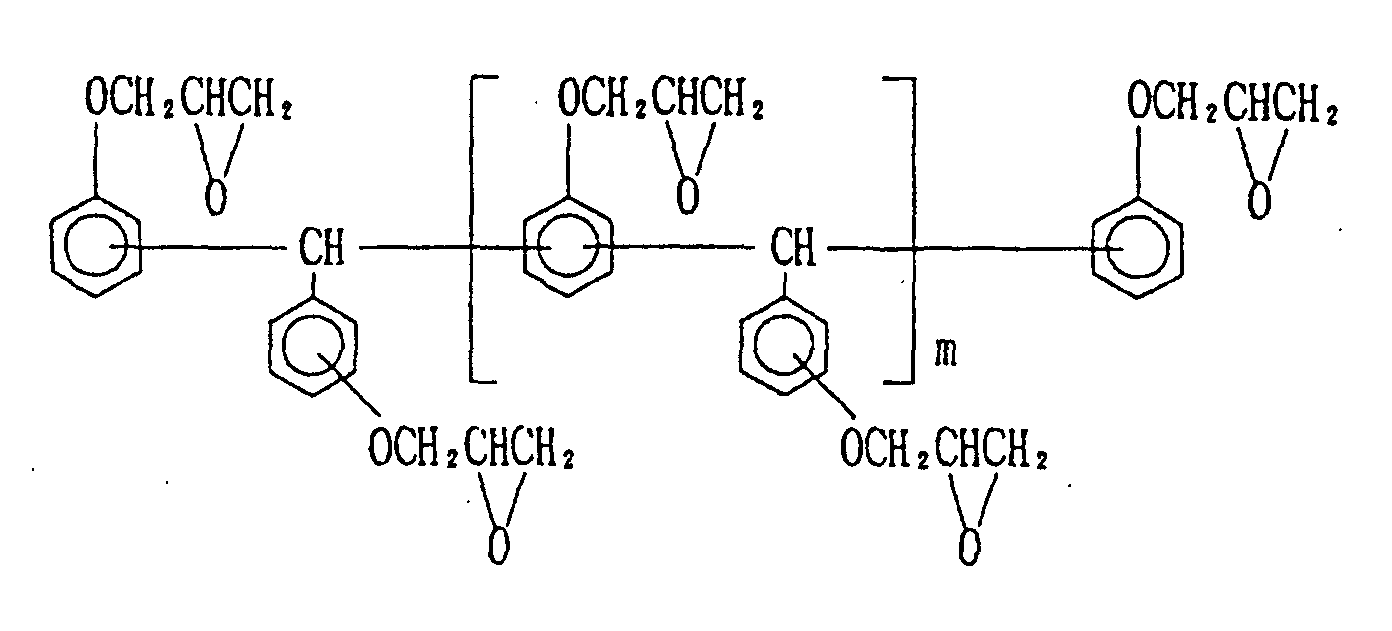
[Epoxy Resin A]
An epoxy resin (epoxy equivalence: 170, softening point: 60°C),
represented by the following formula:
An epoxy resin (epoxy equivalence: 175, melting point: 142°C),
represented by the following formula:
A phenol novolak resin (hydroxyl group equivalence: 105, softening point
60°C)
[Curing Accelerator]
1,5-diazabicyclo[4.3.0]nonene-5 (DBN)
Tetraphenylphosphonium tetraphenylborate (TPP-K)
[Spherical Silica Powder]
Spherical fused silica powder (average particle size: 3 µm)
[Coupling Agent]
γ-Methacryloxypropyltriethoxysilane
Examples A1 to A6
Each of the components shown in Table 1 given below was supplied to a
Henschel mixer in proportions shown in the same table, and the components
were mixed therein for 30 minutes. Thereafter, the resulting mixture was
supplied into a kneading extruder shown in Figure 1 described above, and a
tablet comprising an epoxy resin composition was prepared in the manner
described above. Specifically, the molten resin composition was injected into a
tablet mold (inner diameter: 13 mm, height: 20 mm) with an extrusion force
exerted by the kneading extruder, and the injected resin composition was
pressure molded under a pressure of 1 × 10⁷ Pa, with circulating cooled water in
the mold holder at a temperature of 20°C. The resulting tablet was ejected from
the mold by the upward lunge of the lower plunger, to give an epoxy resin
composition tablet.
Comparative Examples A1 to A3
Each of the components shown in Table 2 given below was formulated in
proportions shown in the same table and melt-kneaded in a mixing roller at a
temperature of 100°C for 3 minutes. The melt-kneaded mixture was cooled and
solidified, and thereafter pulverized and tableted, to give an epoxy resin
composition tablet.
Comparative Example A4
Each of the components shown in Table 2 given below was formulated in
proportions shown in the same table. Each epoxy resin composition tablet was
prepared in the same manner as Examples A1 to A6 so as to have an amount
reduced by heating and a compression ratio as shown in Table 2.
Using each epoxy resin composition tablet as obtained above, the amount
reduced by heating, the compression ratio, the glass transition temperature of the
cured product were respectively determined in accordance with the method
described above. The results are also shown in Tables 1 and 2.
| (parts by weight) |
| Example No. | A1 | A2 | A3 | A4 | A5 | A6 |
| Epoxy Resin A | 100 | 100 | 100 | 100 | 100 | 30 |
| Epoxy Resin B | - | - | - | - | - | 60 |
| Brominated Epoxy Resin | 13 | 13 | - | - | - | 15 |
| Phenol Novolak Resin | 60 | 60 | 60 | 60 | 60 | 60 |
| DBN | 1 | 1 | 1 | 1 | 1 | - |
| TPP-K | - | - | - | - | - | 7 |
| Spherical Silica Powder | 1200 | 680 | 700 | 700 | 700 | 680 |
| Coupling Agent | 1.8 | 1.8 | 1.8 | 1.8 | 1.8 | 1.8 |
| Carbon Black | 7 | 7 | 7 | 7 | 7 | 7 |
| Antimony Trioxide | 11 | 14 | - | - | - | 14 |
| Carnauba Wax | 1 | 1 | 1 | 1 | 1 | 1 |
| Amount Reduced by Heating (% by weight) | 0.04 | 0.03 | 0.03 | 0.02 | 0.03 | 0.04 |
| Compression Ratio (%) | 99.5 | 99.5 | 99.5 | 99.5 | 98.0 | 99.5 |
| Glass Transition Temperature (°C) | 180 | 178 | 178 | 178 | 178 | 145 |
| (parts by weight) |
| Comparative Example No. | A1 | A2 | A3 | A4 |
| Epoxy Resin A | 100 | 100 | 100 | 40 |
| Epoxy Resin B | - | - | - | 80 |
| Brominated Epoxy Resin | - | - | - | - |
| Phenol Novolak Resin | 60 | 60 | 60 | 50 |
| DBN | 1 | 1 | 1 | 1 |
| TPP-K | - | - | - | - |
| Spherical Silica Powder | 700 | 700 | 700 | 700 |
| Coupling Agent | 1.8 | 1.8 | 1.8 | 1.8 |
| Carbon Black | 7 | 7 | 7 | 7 |
| Antimony Trioxide | - | - | - | - |
| Carnauba Wax | 1 | 1 | 1 | 1 |
| Amount Reduced by Heating (% by weight) | 0.06 | 0.15 | 0.19 | 0.12 |
| Compression Ratio (%) | 98.0 | 98.0 | 93.0 | 99.5 |
| Glass Transition Temperature (°C) | 175 | 175 | 175 | 129 |
Thereafter, the wafer with a resin layer was prepared in the following
manner by using each epoxy resin composition tablet obtained above.
Specifically, a wafer comprising a plural projected electrodes was mounted on a
lower mold of the molds for producing a semiconductor device comprising an
upper mold and a lower mold in such a manner that the projected electrodes were
facing the upper mold. At the same time, the above-mentioned epoxy resin
composition tablet was mounted on the wafer, and a film commercially available
from NITTO DENKO CORPORATION under the trade name MPS-31 was
provided between this tablet and the upper mold. Next, an entire mold was
heated to 175°C by using a heater installed in the above-mentioned mold for
producing the semiconductor device, and the tablet was compressed at a pressure
of 9800 N by dropping the upper mold downwardly. A resin layer (uncured) was
formed on a projected electrode-mounting side of the wafer, with compression-deforming
the tablet softened by heating. By repeating the above processes, a
resin layer having a thickness of 100 µm is formed on a side comprising
projected electrodes of the wafer.
Next, the above-mentioned resin layer was cured by heating (175°C), to
form a cured resin layer. Thereafter, the wafer with formed cured resin layers
was taken out of the mold, and the film commercially available from NITTO
DENKO CORPORATION secured to the cured resin layer was peeled off,
whereby exposing tip ends of the projected electrodes in an embedded state to
the film. Thus, there was prepared a wafer with a resin layer as shown in Figure
2 comprising a plural projected electrodes 2 and a cured resin layer 3 formed on
a projected electrode-mounting side of the wafer 1.
Wafer used: 8 inch (20.32 cm) wafer, thickness: 680 µm, made of Si
The bowing of each wafer with a resin layer as obtained above was
determined by the method described below. The results are shown in Tables 3
and 4.
[Determination of Bowing of Wafer with Resin Layer]
The bowing was determined for each of the resulting wafers with a resin
layer by measuring an extent of bowing L shown in Figure 11 using a
microdepth meter. In Figure 11, 3 is a cured resin layer (cured product of an
epoxy resin composition), 1 is a wafer, and 2 is projected electrodes.
| Example No. | Al | A2 | A3 | A4 | A5 | A6 |
| Bowing L (mm) | 1.5 | 1.3 | 1.5 | 1.4 | 1.5 | 1.9 |
| Comparative Example No. | A1 | A2 | A3 | A4 |
| Bowing L (mm) | 2.4 | 3.0 | 4.5 | 5.2 |
As is clear from Tables 3 and 4, it can be seen that the products of
Examples have very small values of bowing as compared with those of
Comparative Examples, so that a wafer with a resin layer having high reliability
can be obtained. Therefore, a semiconductor device obtained by dicing the wafer
with a resin layer of the products of Examples to a given size by a blade dicing
method of course has little bowing and high reliability.
Example B
First, prior to the Examples, each of the following components was
prepared.
[Epoxy Resin A]
The same as Epoxy Resin A in Example A
[Epoxy Resin B]
An epoxy resin (epoxy equivalence: 173, melting point: 100°C),
represented by the following formula:
The same as Epoxy Resin B in Example A
[Curing Agent]
A phenol novolak resin (hydroxyl group equivalence: 105, softening point
60°C)
[Curing Accelerator]
1,5-diazabicyclo[4.3.0]nonene-5 (DBN)
[Spherical Silica Powder]
Spherical fused silica powder (average particle size: 25 µm)
[Composite Metal Hydroxide]
Mg0.8Zn0.2(OH)2 (polyhedral shape, average particle size: 1.7 µm)
[Coupling Agent]
γ-Methacryloxypropyltriethoxysilane
Examples B1 to B6
Each of the components shown in Table 5 given below was supplied to a
Henschel mixer in proportions shown in the same table, and the components
were mixed therein for 30 minutes. Thereafter, the resulting mixture was
supplied into a kneading extruder shown in Figure 1 described above, and a
epoxy resin composition tablet was prepared in the manner described above.
Specifically, the molten resin composition was injected into a tablet mold (inner
diameter: 13 mm, height: 20 mm) with an extrusion force exerted by the
kneading extruder, and the injected resin composition was pressure molded
under a pressure of 980 × 104 Pa, with circulating cooled water in the mold
holder at a temperature of 20°C. The resulting tablet was ejected from the mold
by the upward lunge of the lower plunger, to give an epoxy resin composition
tablet.
Comparative Examples B1 to B5
Each of the components shown in Table 6 given below was formulated in
proportions shown in the same table and melt-kneaded in a mixing roller at a
temperature of 100°C for 3 minutes. The melt-kneaded mixture was cooled and
solidified, and thereafter pulverized and tableted, to give an epoxy resin
composition tablet.
Using each epoxy resin composition tablet as obtained above, the amount
reduced by heating, the compression ratio, the glass transition temperature of the
cured product were respectively determined in accordance with the method
described above. The results are also shown in Tables 5 and 6.
| (parts by weight) |
| Example No. | B1 | B2 | B3 | B4 | B5 | B6 |
| Epoxy Resin A | 100 | 30 | 30 | 30 | 30 | 15 |
| Epoxy Resin B | - | 70 | - | 70 | 70 | - |
| Epoxy Resin C | - | - | 70 | - | - | 85 |
| Phenol Novolak Resin | 66 | 65 | 60 | 60 | 60 | 60 |
| DBN | 1 | 1.5 | 1.5 | 1.5 | 1.5 | 1.5 |
| Brominated Epoxy Resin | 10 | 10 | 10 | - | - | 10 |
| Spherical Silica Powder | 1200 | 1600 | 1500 | 1400 | 1400 | 1600 |
| Composite Metal Hydroxide | - | - | - | 100 | 15 | - |
| Red Phosphorus | - | - | - | - | 1 | - |
| Coupling Agent | 2 | 2 | 2 | 2 | 2 | 2 |
| Carbon Black | 3 | 3 | 3 | 3 | 3 | 3 |
| Antimony Trioxide | 10 | 10 | 10 | - | - | 10 |
| Carnauba Wax | 3 | 3 | 3 | 3 | 3 | 3 |
| Amount Reduced by Heating (% by weight) | 0.04 | 0.03 | 0.03 | 0.03 | 0.04 | 0.03 |
| Compression Ratio (%) | 99.5 | 99.5 | 99.5 | 99.0 | 100 | 100 |
| Glass Transition Temperature (°C) | 180 | 160 | 160 | 160 | 160 | 145 |
| (parts by weight) |
| Comparative Example No. | B1 | B2 | B3 | B4 | B5 |
| Epoxy Resin A | 100 | 100 | 30 | 30 | - |
| Epoxy Resin B | - | - | 70 | 70 | - |
| Epoxy Resin C | - | - | - | - | 100 |
| Phenol Novolak Resin | 66 | 66 | 65 | 65 | 60 |
| DBN | 1 | 1 | 1.5 | 1.5 | 2.0 |
| Brominated Epoxy Resin | 10 | 10 | 10 | 10 | 10 |
| Spherical Silica Powder | 1200 | 1200 | 1600 | 1600 | 1400 |
| Composite Metal Hydroxide | - | - | - | - | - |
| Red Phosphorus | - | - | - | - | - |
| Coupling Agent | 2 | 2 | 2 | 2 | 2 |
| Carbon Black | 3 | 3 | 3 | 3 | 3 |
| Antimony Trioxide | 10 | 10 | 10 | 10 | 10 |
| Carnauba Wax | 3 | 3 | 3 | 3 | 3 |
| Amount Reduced by Heating (% by weight) | 0.06 | 0.11 | 0.08 | 0.09 | 0.06 |
| Compression Ratio (%) | 95.0 | 99.5 | 98.5 | 95.0 | 97.0 |
| Glass Transition Temperature (°C) | 180 | 180 | 160 | 160 | 125 |
Thereafter, a one-sided sealing-type semiconductor device was produced
by using each epoxy resin composition tablet obtained in the manner described
above, and subjecting a semiconductor element mounted on an insulating
substrate to transfer-molding (conditions: 175°C for 2 minutes, and after-curing
of 175°C for 5 hours). The resulting semiconductor device was as follows.
Size of sealed part (cured product of an epoxy resin composition):
35 mm × 35 mm × 1.2 mm in thickness
Size of semiconductor element: 12 mm × 12 mm × 0.4 mm in thickness
Size of insulating substrate: 40 mm × 40 mm × 0.6 mm in thickness
Materials for insulating substrate: bismaleimidotriazine (BT) resin/glass cloth
substrate (commercially available from Mitsubishi Gas Chemical
Company, Inc.)
The bowing of each semiconductor device as obtained above was
determined by the method described below. The results are shown in Tables 7
and 8.
[Determination of Bowing of Semiconductor Device]
The bowing was determined for each of the resulting semiconductor
devices by measuring an extent of bowing L using a microdepth meter shown in
Figure 12. In Figure 12, 3' is a cured product of an epoxy resin composition, 6 is
a semiconductor element, and 5 is an insulating substrate.
| Example No. | B1 | B2 | B3 | B4 | B5 | B6 |
| Bowing L (µm) | 40 | 50 | 50 | 50 | 50 | 65 |
| Comparative Example No. | B1 | B2 | B3 | B4 | B5 |
| Bowing L (µm) | 90 | 120 | 90 | 150 | 210 |
As is clear from Tables 7 and 8, it can be seen that the products of
Examples have very small values of bowing as compared with those of
Comparative Examples, so that a semiconductor device having high reliability
can be obtained.
Example C
First, prior to the Examples, each of the following components was
prepared.
[Epoxy Resin A]
The same as Epoxy Resin A in Example A
[Epoxy Resin B]
The same as Epoxy Resin B in Example A
[Curing Agent]
A phenol novolak resin (hydroxyl group equivalence: 105, softening point
60°C)
[Curing Accelerator]
1,5-diazabicyclo[4.3.0]nonene-5 (DBN)
Tetraphenylphosphonium tetraphenylborate (TPP-K)
[Spherical Silica Powder]
Spherical fused silica powder (average particle size: 5 µm)
[Coupling Agent]
γ-Methacryloxypropyltriethoxysilane
Examples C1 to C6
Each of the components shown in Table 9 given below was supplied to a
Henschel mixer in proportions shown in the same table, and the components
were mixed therein for 30 minutes. Thereafter, the resulting mixture was
supplied into a kneading extruder shown in Figure 2 described above, and an
epoxy resin composition tablet was prepared in the manner described above.
Specifically, the molten resin composition was injected into a tablet mold (inner
diameter: 13 mm, height: 20 mm) with an extrusion force exerted by the
kneading extruder, and the injected resin composition was pressure molded
under a pressure of 1 × 10⁷ Pa, with circulating cooled water in the mold holder
at a temperature of 20°C. The resulting tablet was ejected from the mold by the
upward lunge of the lower plunger, to give an epoxy resin composition tablet.
Comparative Examples C1 to C3
Each of the components shown in Table 10 given below was formulated
in proportions shown in the same table and melt-kneaded in a mixing roller at a
temperature of 100°C for 3 minutes. The melt-kneaded mixture was cooled and
solidified, and thereafter pulverized and tableted, to give an epoxy resin
composition tablet.
Comparative Example C4
Each of the components shown in Table 10 given below was formulated
in proportions shown in the same table. Each epoxy resin composition tablet was
prepared in the same manner as Examples C1 to C6 so as to have an amount
reduced by heating and a compression ratio as shown in Table 10.
Using each epoxy resin composition tablet as obtained above, the amount
reduced by heating, the compression ratio, the glass transition temperature of the
cured product were respectively determined in accordance with the method
described above. The results are also shown in Tables 9 and 10.
| (parts by weight) |
| Example No. | C1 | C2 | C3 | C4 | C5 | C6 |
| Epoxy Resin A | 100 | 100 | 100 | 100 | 100 | 30 |
| Epoxy Resin B | - | - | - | - | - | 60 |
| Brominated Epoxy Resin | 13 | 13 | - | - | - | 15 |
| Phenol Novolak Resin | 60 | 60 | 60 | 60 | 60 | 60 |
| DBN | 1 | 1 | 1 | 1 | 1 | - |
| TPP-K | - | - | - | - | - | 7 |
| Spherical Silica Powder | 1200 | 680 | 700 | 700 | 700 | 680 |
| Coupling Agent | 1.8 | 1.8 | 1.8 | 1.8 | 1.8 | 1.8 |
| Carbon Black | 7 | 7 | 7 | 7 | 7 | 7 |
| Antimony Trioxide | 11 | 14 | - | - | - | 14 |
| Carnauba Wax | 1 | 1 | 1 | 1 | 1 | 1 |
| Amount Reduced by Heating (% by weight) | 0.04 | 0.03 | 0.02 | 0.02 | 0.02 | 0.04 |
| Compression Ratio (%) | 99.5 | 99.5 | 99.5 | 99.5 | 98.0 | 99.5 |
| Glass Transition Temperature (°C) | 180 | 178 | 178 | 178 | 178 | 145 |
| (parts by weight) |
| Comparative Example No. | C1 | C2 | C3 | C4 |
| Epoxy Resin A | 100 | 100 | 100 | 40 |
| Epoxy Resin B | - | - | - | 80 |
| Brominated Epoxy Resin | - | - | - | - |
| Phenol Novolak Resin | 60 | 60 | 60 | 50 |
| DBN | 1 | 1 | 1 | 1 |
| TPP-K | - | - | - | - |
| Spherical Silica Powder | 700 | 700 | 700 | 700 |
| Coupling Agent | 1.8 | 1.8 | 1.8 | 1.8 |
| Carbon Black | 7 | 7 | 7 | 7 |
| Antimony Trioxide | - | - | - | - |
| Carnauba Wax | 1 | 1 | 1 | 1 |
| Amount Reduced by Heating (% by weight) | 0.06 | 0.15 | 0.19 | 0.12 |
| Compression Ratio (%) | 98 | 98 | 93 | 99.5 |
| Glass Transition Temperature (°C) | 175 | 175 | 175 | 129 |
Thereafter, a semiconductor device was prepared in the following manner
by using each epoxy resin composition tablet obtained above. Specifically, as
shown in Figure 8, a semiconductor element 6 was mounted on an insulating
substrate 5 on which a plural spherical connecting electrodes 4 were provided.
Next, a specified epoxy resin composition tablet was supplied into a molding
machine, thereafter this tablet was heated and molted to give a molten state, and
the molten tablet was pressed. As described above, the void between the above-mentioned
semiconductor element 6 and the above-mentioned insulating
substrate 5 was filled with the molten resin described above, and the molten resin
was cured to seal the void with the cured resin, thereby forming a cured resin
layer 3. As described above, a semiconductor device was prepared. The
temperature for heating and melting mentioned above was 175°C, and the
pressing condition was adjusted to 600 Pa/one element.
Distance of the cured resin layer (distance in voids): 100 µm
Size of semiconductor element: 15 mm × 15 mm × 370 µm in thickness
Size of insulating substrate: 20 mm × 20 mm x 0.4 mm in thickness
Materials for insulating substrate: bismaleimidotriazine (BT) resin/glass cloth
substrate (commercially available from Mitsubishi Gas Chemical Company, Inc.).
The bowing of each semiconductor device as obtained above was
determined by the method described below. The results are shown in Tables 11
and 12.
[Determination of Bowing of Semiconductor]
The bowing was determined for each of the resulting semiconductors by
measuring an extent of bowing L using a microdepth meter shown in Figure 13.
In Figure 13, 5 is an insulating substrate, 4 is connecting electrodes, 6 is a
semiconductor element, and 3 is a cured resin layer (cured product of an epoxy
resin composition).
| Example No. | C1 | C2 | C3 | C4 | C5 | C6 |
| Bowing L (µm) | 30 | 50 | 50 | 40 | 40 | 30 |
| Comparative Example No. | C1 | C2 | C3 | C4 |
| Bowing L (µm) | 110 | 150 | 100 | 100 |
As is clear from Tables 11 and 12, it can be seen that the products of
Examples have very small values of bowing as compared with those of
Comparative Examples, so that a semiconductor device having high reliability
can be obtained.
EQUIVALENTS
The present invention being thus described, it will be obvious that the
same may be varied in many ways. Such variations are not to be regarded as a
departure from the spirit and scope of the invention, and all such modifications
as would be obvious to one skilled in the art are intended to be included within
the scope of the following claims.