EP1138656A1 - Silicon nitride member, method for manufacturing the same, and cutting tool - Google Patents
Silicon nitride member, method for manufacturing the same, and cutting tool Download PDFInfo
- Publication number
- EP1138656A1 EP1138656A1 EP01303041A EP01303041A EP1138656A1 EP 1138656 A1 EP1138656 A1 EP 1138656A1 EP 01303041 A EP01303041 A EP 01303041A EP 01303041 A EP01303041 A EP 01303041A EP 1138656 A1 EP1138656 A1 EP 1138656A1
- Authority
- EP
- European Patent Office
- Prior art keywords
- substrate
- silicon nitride
- sintering
- measured
- weight
- Prior art date
- Legal status (The legal status is an assumption and is not a legal conclusion. Google has not performed a legal analysis and makes no representation as to the accuracy of the status listed.)
- Granted
Links
- 229910052581 Si3N4 Inorganic materials 0.000 title claims abstract description 71
- HQVNEWCFYHHQES-UHFFFAOYSA-N silicon nitride Chemical compound N12[Si]34N5[Si]62N3[Si]51N64 HQVNEWCFYHHQES-UHFFFAOYSA-N 0.000 title claims abstract description 67
- 238000005520 cutting process Methods 0.000 title claims abstract description 52
- 238000000034 method Methods 0.000 title claims abstract description 25
- 238000004519 manufacturing process Methods 0.000 title claims abstract description 12
- 239000000758 substrate Substances 0.000 claims abstract description 130
- 238000005245 sintering Methods 0.000 claims abstract description 48
- 239000000463 material Substances 0.000 claims abstract description 14
- 238000010438 heat treatment Methods 0.000 claims description 9
- 239000012299 nitrogen atmosphere Substances 0.000 claims description 6
- 238000000576 coating method Methods 0.000 abstract description 17
- 239000011248 coating agent Substances 0.000 abstract description 16
- 230000006735 deficit Effects 0.000 abstract description 8
- 230000000052 comparative effect Effects 0.000 description 20
- 238000005452 bending Methods 0.000 description 11
- 239000010410 layer Substances 0.000 description 8
- PNEYBMLMFCGWSK-UHFFFAOYSA-N aluminium oxide Inorganic materials [O-2].[O-2].[O-2].[Al+3].[Al+3] PNEYBMLMFCGWSK-UHFFFAOYSA-N 0.000 description 6
- 229910052593 corundum Inorganic materials 0.000 description 6
- 229910001845 yogo sapphire Inorganic materials 0.000 description 6
- LFQSCWFLJHTTHZ-UHFFFAOYSA-N Ethanol Chemical compound CCO LFQSCWFLJHTTHZ-UHFFFAOYSA-N 0.000 description 4
- 238000005229 chemical vapour deposition Methods 0.000 description 4
- 230000001771 impaired effect Effects 0.000 description 4
- 238000004458 analytical method Methods 0.000 description 3
- 239000000203 mixture Substances 0.000 description 3
- 238000005240 physical vapour deposition Methods 0.000 description 3
- 239000002002 slurry Substances 0.000 description 3
- -1 α-Si3N4 Chemical compound 0.000 description 3
- ATJFFYVFTNAWJD-UHFFFAOYSA-N Tin Chemical compound [Sn] ATJFFYVFTNAWJD-UHFFFAOYSA-N 0.000 description 2
- MCMNRKCIXSYSNV-UHFFFAOYSA-N Zirconium dioxide Chemical compound O=[Zr]=O MCMNRKCIXSYSNV-UHFFFAOYSA-N 0.000 description 2
- 239000000919 ceramic Substances 0.000 description 2
- 230000000694 effects Effects 0.000 description 2
- 230000001747 exhibiting effect Effects 0.000 description 2
- 239000007789 gas Substances 0.000 description 2
- 238000000227 grinding Methods 0.000 description 2
- 238000013001 point bending Methods 0.000 description 2
- FIXNOXLJNSSSLJ-UHFFFAOYSA-N ytterbium(III) oxide Inorganic materials O=[Yb]O[Yb]=O FIXNOXLJNSSSLJ-UHFFFAOYSA-N 0.000 description 2
- IJGRMHOSHXDMSA-UHFFFAOYSA-N Atomic nitrogen Chemical compound N#N IJGRMHOSHXDMSA-UHFFFAOYSA-N 0.000 description 1
- 229910001018 Cast iron Inorganic materials 0.000 description 1
- 239000012298 atmosphere Substances 0.000 description 1
- 239000011230 binding agent Substances 0.000 description 1
- 238000001816 cooling Methods 0.000 description 1
- 238000000354 decomposition reaction Methods 0.000 description 1
- 230000007423 decrease Effects 0.000 description 1
- 230000003247 decreasing effect Effects 0.000 description 1
- 238000000151 deposition Methods 0.000 description 1
- 230000008021 deposition Effects 0.000 description 1
- 229910001873 dinitrogen Inorganic materials 0.000 description 1
- 238000005516 engineering process Methods 0.000 description 1
- VQCBHWLJZDBHOS-UHFFFAOYSA-N erbium(III) oxide Inorganic materials O=[Er]O[Er]=O VQCBHWLJZDBHOS-UHFFFAOYSA-N 0.000 description 1
- 238000002474 experimental method Methods 0.000 description 1
- 239000011521 glass Substances 0.000 description 1
- 238000010191 image analysis Methods 0.000 description 1
- CPLXHLVBOLITMK-UHFFFAOYSA-N magnesium oxide Inorganic materials [Mg]=O CPLXHLVBOLITMK-UHFFFAOYSA-N 0.000 description 1
- 238000005457 optimization Methods 0.000 description 1
- 238000005498 polishing Methods 0.000 description 1
- 239000000843 powder Substances 0.000 description 1
- 238000001878 scanning electron micrograph Methods 0.000 description 1
- 239000002356 single layer Substances 0.000 description 1
- 239000002904 solvent Substances 0.000 description 1
- 238000001694 spray drying Methods 0.000 description 1
- 230000001629 suppression Effects 0.000 description 1
- RUDFQVOCFDJEEF-UHFFFAOYSA-N yttrium(III) oxide Inorganic materials [O-2].[O-2].[O-2].[Y+3].[Y+3] RUDFQVOCFDJEEF-UHFFFAOYSA-N 0.000 description 1
Images

Classifications
-
- C—CHEMISTRY; METALLURGY
- C04—CEMENTS; CONCRETE; ARTIFICIAL STONE; CERAMICS; REFRACTORIES
- C04B—LIME, MAGNESIA; SLAG; CEMENTS; COMPOSITIONS THEREOF, e.g. MORTARS, CONCRETE OR LIKE BUILDING MATERIALS; ARTIFICIAL STONE; CERAMICS; REFRACTORIES; TREATMENT OF NATURAL STONE
- C04B35/00—Shaped ceramic products characterised by their composition; Ceramics compositions; Processing powders of inorganic compounds preparatory to the manufacturing of ceramic products
- C04B35/515—Shaped ceramic products characterised by their composition; Ceramics compositions; Processing powders of inorganic compounds preparatory to the manufacturing of ceramic products based on non-oxide ceramics
- C04B35/58—Shaped ceramic products characterised by their composition; Ceramics compositions; Processing powders of inorganic compounds preparatory to the manufacturing of ceramic products based on non-oxide ceramics based on borides, nitrides, i.e. nitrides, oxynitrides, carbonitrides or oxycarbonitrides or silicides
- C04B35/584—Shaped ceramic products characterised by their composition; Ceramics compositions; Processing powders of inorganic compounds preparatory to the manufacturing of ceramic products based on non-oxide ceramics based on borides, nitrides, i.e. nitrides, oxynitrides, carbonitrides or oxycarbonitrides or silicides based on silicon nitride
-
- C—CHEMISTRY; METALLURGY
- C04—CEMENTS; CONCRETE; ARTIFICIAL STONE; CERAMICS; REFRACTORIES
- C04B—LIME, MAGNESIA; SLAG; CEMENTS; COMPOSITIONS THEREOF, e.g. MORTARS, CONCRETE OR LIKE BUILDING MATERIALS; ARTIFICIAL STONE; CERAMICS; REFRACTORIES; TREATMENT OF NATURAL STONE
- C04B41/00—After-treatment of mortars, concrete, artificial stone or ceramics; Treatment of natural stone
- C04B41/009—After-treatment of mortars, concrete, artificial stone or ceramics; Treatment of natural stone characterised by the material treated
-
- C—CHEMISTRY; METALLURGY
- C04—CEMENTS; CONCRETE; ARTIFICIAL STONE; CERAMICS; REFRACTORIES
- C04B—LIME, MAGNESIA; SLAG; CEMENTS; COMPOSITIONS THEREOF, e.g. MORTARS, CONCRETE OR LIKE BUILDING MATERIALS; ARTIFICIAL STONE; CERAMICS; REFRACTORIES; TREATMENT OF NATURAL STONE
- C04B35/00—Shaped ceramic products characterised by their composition; Ceramics compositions; Processing powders of inorganic compounds preparatory to the manufacturing of ceramic products
- C04B35/515—Shaped ceramic products characterised by their composition; Ceramics compositions; Processing powders of inorganic compounds preparatory to the manufacturing of ceramic products based on non-oxide ceramics
- C04B35/58—Shaped ceramic products characterised by their composition; Ceramics compositions; Processing powders of inorganic compounds preparatory to the manufacturing of ceramic products based on non-oxide ceramics based on borides, nitrides, i.e. nitrides, oxynitrides, carbonitrides or oxycarbonitrides or silicides
- C04B35/584—Shaped ceramic products characterised by their composition; Ceramics compositions; Processing powders of inorganic compounds preparatory to the manufacturing of ceramic products based on non-oxide ceramics based on borides, nitrides, i.e. nitrides, oxynitrides, carbonitrides or oxycarbonitrides or silicides based on silicon nitride
- C04B35/593—Shaped ceramic products characterised by their composition; Ceramics compositions; Processing powders of inorganic compounds preparatory to the manufacturing of ceramic products based on non-oxide ceramics based on borides, nitrides, i.e. nitrides, oxynitrides, carbonitrides or oxycarbonitrides or silicides based on silicon nitride obtained by pressure sintering
- C04B35/5935—Shaped ceramic products characterised by their composition; Ceramics compositions; Processing powders of inorganic compounds preparatory to the manufacturing of ceramic products based on non-oxide ceramics based on borides, nitrides, i.e. nitrides, oxynitrides, carbonitrides or oxycarbonitrides or silicides based on silicon nitride obtained by pressure sintering obtained by gas pressure sintering
-
- C—CHEMISTRY; METALLURGY
- C04—CEMENTS; CONCRETE; ARTIFICIAL STONE; CERAMICS; REFRACTORIES
- C04B—LIME, MAGNESIA; SLAG; CEMENTS; COMPOSITIONS THEREOF, e.g. MORTARS, CONCRETE OR LIKE BUILDING MATERIALS; ARTIFICIAL STONE; CERAMICS; REFRACTORIES; TREATMENT OF NATURAL STONE
- C04B41/00—After-treatment of mortars, concrete, artificial stone or ceramics; Treatment of natural stone
- C04B41/45—Coating or impregnating, e.g. injection in masonry, partial coating of green or fired ceramics, organic coating compositions for adhering together two concrete elements
- C04B41/52—Multiple coating or impregnating multiple coating or impregnating with the same composition or with compositions only differing in the concentration of the constituents, is classified as single coating or impregnation
-
- C—CHEMISTRY; METALLURGY
- C04—CEMENTS; CONCRETE; ARTIFICIAL STONE; CERAMICS; REFRACTORIES
- C04B—LIME, MAGNESIA; SLAG; CEMENTS; COMPOSITIONS THEREOF, e.g. MORTARS, CONCRETE OR LIKE BUILDING MATERIALS; ARTIFICIAL STONE; CERAMICS; REFRACTORIES; TREATMENT OF NATURAL STONE
- C04B41/00—After-treatment of mortars, concrete, artificial stone or ceramics; Treatment of natural stone
- C04B41/80—After-treatment of mortars, concrete, artificial stone or ceramics; Treatment of natural stone of only ceramics
- C04B41/81—Coating or impregnation
- C04B41/89—Coating or impregnation for obtaining at least two superposed coatings having different compositions
-
- C—CHEMISTRY; METALLURGY
- C04—CEMENTS; CONCRETE; ARTIFICIAL STONE; CERAMICS; REFRACTORIES
- C04B—LIME, MAGNESIA; SLAG; CEMENTS; COMPOSITIONS THEREOF, e.g. MORTARS, CONCRETE OR LIKE BUILDING MATERIALS; ARTIFICIAL STONE; CERAMICS; REFRACTORIES; TREATMENT OF NATURAL STONE
- C04B2235/00—Aspects relating to ceramic starting mixtures or sintered ceramic products
- C04B2235/02—Composition of constituents of the starting material or of secondary phases of the final product
- C04B2235/30—Constituents and secondary phases not being of a fibrous nature
- C04B2235/32—Metal oxides, mixed metal oxides, or oxide-forming salts thereof, e.g. carbonates, nitrates, (oxy)hydroxides, chlorides
- C04B2235/3205—Alkaline earth oxides or oxide forming salts thereof, e.g. beryllium oxide
- C04B2235/3206—Magnesium oxides or oxide-forming salts thereof
-
- C—CHEMISTRY; METALLURGY
- C04—CEMENTS; CONCRETE; ARTIFICIAL STONE; CERAMICS; REFRACTORIES
- C04B—LIME, MAGNESIA; SLAG; CEMENTS; COMPOSITIONS THEREOF, e.g. MORTARS, CONCRETE OR LIKE BUILDING MATERIALS; ARTIFICIAL STONE; CERAMICS; REFRACTORIES; TREATMENT OF NATURAL STONE
- C04B2235/00—Aspects relating to ceramic starting mixtures or sintered ceramic products
- C04B2235/02—Composition of constituents of the starting material or of secondary phases of the final product
- C04B2235/30—Constituents and secondary phases not being of a fibrous nature
- C04B2235/32—Metal oxides, mixed metal oxides, or oxide-forming salts thereof, e.g. carbonates, nitrates, (oxy)hydroxides, chlorides
- C04B2235/3217—Aluminum oxide or oxide forming salts thereof, e.g. bauxite, alpha-alumina
-
- C—CHEMISTRY; METALLURGY
- C04—CEMENTS; CONCRETE; ARTIFICIAL STONE; CERAMICS; REFRACTORIES
- C04B—LIME, MAGNESIA; SLAG; CEMENTS; COMPOSITIONS THEREOF, e.g. MORTARS, CONCRETE OR LIKE BUILDING MATERIALS; ARTIFICIAL STONE; CERAMICS; REFRACTORIES; TREATMENT OF NATURAL STONE
- C04B2235/00—Aspects relating to ceramic starting mixtures or sintered ceramic products
- C04B2235/02—Composition of constituents of the starting material or of secondary phases of the final product
- C04B2235/30—Constituents and secondary phases not being of a fibrous nature
- C04B2235/32—Metal oxides, mixed metal oxides, or oxide-forming salts thereof, e.g. carbonates, nitrates, (oxy)hydroxides, chlorides
- C04B2235/3224—Rare earth oxide or oxide forming salts thereof, e.g. scandium oxide
-
- C—CHEMISTRY; METALLURGY
- C04—CEMENTS; CONCRETE; ARTIFICIAL STONE; CERAMICS; REFRACTORIES
- C04B—LIME, MAGNESIA; SLAG; CEMENTS; COMPOSITIONS THEREOF, e.g. MORTARS, CONCRETE OR LIKE BUILDING MATERIALS; ARTIFICIAL STONE; CERAMICS; REFRACTORIES; TREATMENT OF NATURAL STONE
- C04B2235/00—Aspects relating to ceramic starting mixtures or sintered ceramic products
- C04B2235/02—Composition of constituents of the starting material or of secondary phases of the final product
- C04B2235/30—Constituents and secondary phases not being of a fibrous nature
- C04B2235/38—Non-oxide ceramic constituents or additives
- C04B2235/3852—Nitrides, e.g. oxynitrides, carbonitrides, oxycarbonitrides, lithium nitride, magnesium nitride
- C04B2235/3873—Silicon nitrides, e.g. silicon carbonitride, silicon oxynitride
- C04B2235/3878—Alpha silicon nitrides
-
- C—CHEMISTRY; METALLURGY
- C04—CEMENTS; CONCRETE; ARTIFICIAL STONE; CERAMICS; REFRACTORIES
- C04B—LIME, MAGNESIA; SLAG; CEMENTS; COMPOSITIONS THEREOF, e.g. MORTARS, CONCRETE OR LIKE BUILDING MATERIALS; ARTIFICIAL STONE; CERAMICS; REFRACTORIES; TREATMENT OF NATURAL STONE
- C04B2235/00—Aspects relating to ceramic starting mixtures or sintered ceramic products
- C04B2235/02—Composition of constituents of the starting material or of secondary phases of the final product
- C04B2235/50—Constituents or additives of the starting mixture chosen for their shape or used because of their shape or their physical appearance
- C04B2235/54—Particle size related information
- C04B2235/5418—Particle size related information expressed by the size of the particles or aggregates thereof
- C04B2235/5445—Particle size related information expressed by the size of the particles or aggregates thereof submicron sized, i.e. from 0,1 to 1 micron
-
- C—CHEMISTRY; METALLURGY
- C04—CEMENTS; CONCRETE; ARTIFICIAL STONE; CERAMICS; REFRACTORIES
- C04B—LIME, MAGNESIA; SLAG; CEMENTS; COMPOSITIONS THEREOF, e.g. MORTARS, CONCRETE OR LIKE BUILDING MATERIALS; ARTIFICIAL STONE; CERAMICS; REFRACTORIES; TREATMENT OF NATURAL STONE
- C04B2235/00—Aspects relating to ceramic starting mixtures or sintered ceramic products
- C04B2235/65—Aspects relating to heat treatments of ceramic bodies such as green ceramics or pre-sintered ceramics, e.g. burning, sintering or melting processes
- C04B2235/656—Aspects relating to heat treatments of ceramic bodies such as green ceramics or pre-sintered ceramics, e.g. burning, sintering or melting processes characterised by specific heating conditions during heat treatment
- C04B2235/6567—Treatment time
-
- C—CHEMISTRY; METALLURGY
- C04—CEMENTS; CONCRETE; ARTIFICIAL STONE; CERAMICS; REFRACTORIES
- C04B—LIME, MAGNESIA; SLAG; CEMENTS; COMPOSITIONS THEREOF, e.g. MORTARS, CONCRETE OR LIKE BUILDING MATERIALS; ARTIFICIAL STONE; CERAMICS; REFRACTORIES; TREATMENT OF NATURAL STONE
- C04B2235/00—Aspects relating to ceramic starting mixtures or sintered ceramic products
- C04B2235/65—Aspects relating to heat treatments of ceramic bodies such as green ceramics or pre-sintered ceramics, e.g. burning, sintering or melting processes
- C04B2235/658—Atmosphere during thermal treatment
- C04B2235/6581—Total pressure below 1 atmosphere, e.g. vacuum
-
- C—CHEMISTRY; METALLURGY
- C04—CEMENTS; CONCRETE; ARTIFICIAL STONE; CERAMICS; REFRACTORIES
- C04B—LIME, MAGNESIA; SLAG; CEMENTS; COMPOSITIONS THEREOF, e.g. MORTARS, CONCRETE OR LIKE BUILDING MATERIALS; ARTIFICIAL STONE; CERAMICS; REFRACTORIES; TREATMENT OF NATURAL STONE
- C04B2235/00—Aspects relating to ceramic starting mixtures or sintered ceramic products
- C04B2235/65—Aspects relating to heat treatments of ceramic bodies such as green ceramics or pre-sintered ceramics, e.g. burning, sintering or melting processes
- C04B2235/66—Specific sintering techniques, e.g. centrifugal sintering
- C04B2235/661—Multi-step sintering
- C04B2235/662—Annealing after sintering
-
- C—CHEMISTRY; METALLURGY
- C04—CEMENTS; CONCRETE; ARTIFICIAL STONE; CERAMICS; REFRACTORIES
- C04B—LIME, MAGNESIA; SLAG; CEMENTS; COMPOSITIONS THEREOF, e.g. MORTARS, CONCRETE OR LIKE BUILDING MATERIALS; ARTIFICIAL STONE; CERAMICS; REFRACTORIES; TREATMENT OF NATURAL STONE
- C04B2235/00—Aspects relating to ceramic starting mixtures or sintered ceramic products
- C04B2235/70—Aspects relating to sintered or melt-casted ceramic products
- C04B2235/74—Physical characteristics
- C04B2235/75—Products with a concentration gradient
-
- C—CHEMISTRY; METALLURGY
- C04—CEMENTS; CONCRETE; ARTIFICIAL STONE; CERAMICS; REFRACTORIES
- C04B—LIME, MAGNESIA; SLAG; CEMENTS; COMPOSITIONS THEREOF, e.g. MORTARS, CONCRETE OR LIKE BUILDING MATERIALS; ARTIFICIAL STONE; CERAMICS; REFRACTORIES; TREATMENT OF NATURAL STONE
- C04B2235/00—Aspects relating to ceramic starting mixtures or sintered ceramic products
- C04B2235/70—Aspects relating to sintered or melt-casted ceramic products
- C04B2235/80—Phases present in the sintered or melt-cast ceramic products other than the main phase
- C04B2235/85—Intergranular or grain boundary phases
-
- C—CHEMISTRY; METALLURGY
- C04—CEMENTS; CONCRETE; ARTIFICIAL STONE; CERAMICS; REFRACTORIES
- C04B—LIME, MAGNESIA; SLAG; CEMENTS; COMPOSITIONS THEREOF, e.g. MORTARS, CONCRETE OR LIKE BUILDING MATERIALS; ARTIFICIAL STONE; CERAMICS; REFRACTORIES; TREATMENT OF NATURAL STONE
- C04B2235/00—Aspects relating to ceramic starting mixtures or sintered ceramic products
- C04B2235/70—Aspects relating to sintered or melt-casted ceramic products
- C04B2235/96—Properties of ceramic products, e.g. mechanical properties such as strength, toughness, wear resistance
-
- Y—GENERAL TAGGING OF NEW TECHNOLOGICAL DEVELOPMENTS; GENERAL TAGGING OF CROSS-SECTIONAL TECHNOLOGIES SPANNING OVER SEVERAL SECTIONS OF THE IPC; TECHNICAL SUBJECTS COVERED BY FORMER USPC CROSS-REFERENCE ART COLLECTIONS [XRACs] AND DIGESTS
- Y10—TECHNICAL SUBJECTS COVERED BY FORMER USPC
- Y10T—TECHNICAL SUBJECTS COVERED BY FORMER US CLASSIFICATION
- Y10T428/00—Stock material or miscellaneous articles
- Y10T428/24—Structurally defined web or sheet [e.g., overall dimension, etc.]
- Y10T428/24942—Structurally defined web or sheet [e.g., overall dimension, etc.] including components having same physical characteristic in differing degree
-
- Y—GENERAL TAGGING OF NEW TECHNOLOGICAL DEVELOPMENTS; GENERAL TAGGING OF CROSS-SECTIONAL TECHNOLOGIES SPANNING OVER SEVERAL SECTIONS OF THE IPC; TECHNICAL SUBJECTS COVERED BY FORMER USPC CROSS-REFERENCE ART COLLECTIONS [XRACs] AND DIGESTS
- Y10—TECHNICAL SUBJECTS COVERED BY FORMER USPC
- Y10T—TECHNICAL SUBJECTS COVERED BY FORMER US CLASSIFICATION
- Y10T428/00—Stock material or miscellaneous articles
- Y10T428/31—Surface property or characteristic of web, sheet or block
Definitions
- the present invention relates to a silicon nitride member including a substrate formed through sintering of a silicon nitride material, and a hard film formed on the surface of the substrate, as well as to a method for manufacturing the same and to a cutting tool.
- the surface of a substrate of, for example, a sintered silicon nitride member is coated with a hard film composed of hard components, such as TiCN.
- Examples of the above-mentioned coating method include a CVD (chemical vapor deposition) process and a PVD (physical vapor deposition) process, in which hard components are deposited on the substrate surface to thereby form a hard film on the same.
- CVD chemical vapor deposition
- PVD physical vapor deposition
- the cutting tool (a coated tool) exhibited significantly enhanced wear resistance.
- hard components are deposited at high temperature, thus involving the following problems: because of difference in coefficient of thermal expansion between the hard film and the substrate, stress remains in the substrate surface; and high temperature employed during deposition modifies the substrate surface. As a result, the strength of the substrate coated with the hard film is impaired as compared with that of the bare substrate.
- the present invention has been achieved in view of the above problems, and an object of the present invention is to provide a silicon nitride member exhibiting little impairment in strength even when a substrate thereof is coated with a hard film, and exhibiting excellent resistance to chipping and wear resistance, as well as to provide a method for manufacturing the same and to provide a cutting tool.
- the present inventors have conducted extensive studies on a silicon nitride member in an attempt to minimize impairment in the strength of a substrate thereof coated with a hard film (a coating film) as compared with that of the bare substrate, and have found the following.
- a tensile stress remaining in the substrate surface is the primary cause for impairment in the strength of the substrate of a silicon nitride member (a sintered member) obtained through sintering.
- a silicon nitride member a sintered member obtained through sintering.
- the difference in coefficient of thermal expansion between the hard film (high coefficient of thermal expansion) and the substrate (low coefficient of thermal expansion) causes the residual stress.
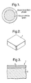
- a silicon nitride member is caused to assume a composition of high sintering-aid content, or a composition of low sintering-aid content, as mentioned above, combined with optimization of sintering conditions, to thereby suppress to the utmost extent volatilization of a grain boundary phase (a glass phase of sintering aids formed on the surface of a silicon nitride grain) formed on the substrate surface as schematically shown in FIG. 1 of the accompanying drawings.
- a cutting tool formed of a silicon nitride member having the above-mentioned properties exhibits excellent wear resistance and resistance to chipping, and is thus favorably applicable not only to normal cutting but also to heavy cutting, which involves a heavy cutting load.
- the aforementioned silicon nitride member having excellent wear resistance and resistance to chipping is applicable not only to cutting tools but also, for example, to wear resistant members of automobile engine components and rotary tools, such as drills and end mills.
- silicon nitride material examples include sialon and a mixture of silicon nitride, such as ⁇ -Si 3 N 4 , and sintering aids, such as MgO, Al 2 O 3 , Yb 2 O 3 , Y 2 O 3 , ZrO 2 , Hf 2 O 3 , and Er 2 O 3 .
- Hard components serving as material for the hard film include Al 2 O 3 , TiCN, TiN, and TiC.
- the hard film may assume the form of a single layer of a single hard component or a multilayer of the same hard component or different hard components.
- Embodiments of a silicon nitride member, a method for manufacturing the same, and a cutting tool according to the present invention will next be described.
- the samples of the Examples exhibit a strength ratio not less than 70, indicating a low impairment in strength after coating with the hard film.
- the samples also exhibit a small amount of flank wear not greater than 0.2 mm and a small amount of notch wear not greater than 0.22 mm.
- the cutting tools of the Examples have excellent resistance to chipping and wear resistance and are thus favorably applicable not only to normal cutting but also, for example, to heavy cutting.
- Comparative Example Nos. 1, 2, 5, 8, 11, and 15 respectively exhibit a volatilization rate of 1, 1.1, 1.3, 1.3, 1.3, and 1.3% by weight and an amount of grain boundary phase of 90%, 89%, 80%, 80%, 81%, and 86% by volume as measured at the substrate surface.
- the samples of the Comparative Examples exhibit a high strength ratio of 94.6, 92.2, 92.7, 95, 93.3, and 91.1.
- the samples exhibit a large amount of flank wear of 0.35, 0.35, 0.34, 0.33, 0.32, and 0.33 mm and a large amount of notch wear of 0.31, 0.39, 0.35, 0.35, 0.33, and 0.4 mm.
- the cutting tools of the Comparative Examples fail to exhibit sufficiently high resistance to wear.
- Comparative Example Nos. 7, 10, and 16 respectively exhibit a volatilization rate of 3.7, 4, and 4% by weight and an amount of grain boundary phase of 48%, 40%, and 42% by volume as measured at the substrate surface.
- the samples of the Comparative Examples exhibit a low strength ratio of 55.5, 54.9, and 51.3, although the samples exhibit a small amount of flank wear of 0.12, 0.13, and 0.13 mm and a small amount of notch wear of 0.11, 0.13, and 0.18 mm.
- the cutting tools of the Comparative Examples exhibit impaired resistance to chipping.
- Comparative Example No. 17 could not be evaluated, since silicon nitride was decomposed due to high heating temperature.
- the present invention is applicable not only to a square plate-like cutting tool but also to a triangular plate-like cutting tool.
- the silicon nitride member of the present invention exhibits merely a slight impairment in strength as measured after coating with the hard film, and thus has high wear resistance and high resistance to chipping.
- a silicon nitride member having high wear resistance and high resistance to chipping can be readily manufactured.
- a cutting tool formed of the thus-manufactured silicon nitride member can exhibit long life under heavy-load working conditions.
Landscapes
- Chemical & Material Sciences (AREA)
- Engineering & Computer Science (AREA)
- Ceramic Engineering (AREA)
- Materials Engineering (AREA)
- Structural Engineering (AREA)
- Organic Chemistry (AREA)
- Manufacturing & Machinery (AREA)
- Ceramic Products (AREA)
- Cutting Tools, Boring Holders, And Turrets (AREA)
Abstract
Description
| Sample No. | Heat Treatment Conditions | |||
| Temp. [°C] | Time [min] | Pressure [kPa] | ||
| Comparative Example | 1 | 1500 | 180 | 6.5 |
| 2 | 240 | |||
| Example | 3 | 1550 | 60 | |
| 4 | ||||
| Comparative Example | 5 | 26 | ||
| Example | 6 | 180 | 6.5 | |
| Comparative Example | 7 | 240 | ||
| 8 | 1600 | 30 | ||
| Example | 9 | 120 | ||
| Comparative Example | 10 | 240 | ||
| 11 | 1650 | 30 | ||
| Example | 12 | 60 | ||
| 13 | 180 | |||
| 14 | 13 | |||
| Comparative Example | 15 | 26 | ||
| 16 | 1700 | 30 | 13 | |
| 17 | 60 |

Claims (7)
- A silicon nitride member comprising a substrate formed through sintering of a silicon nitride material, and a hard film formed on a surface of said substrate, said silicon nitride member characterized in that:
when the strength of said substrate as measured before said substrate is coated with said hard film is taken as 100%, the strength of said silicon nitride member as measured after said substrate is coated with said hard film is 70% to 95%. - A silicon nitride member according to Claim 1, wherein a change in weight of said substrate associated with sintering is 1.5% to 3.5% by weight.
- A silicon nitride member comprising a substrate formed through sintering of a silicon nitride material, and a hard film formed on a surface of said substrate, said silicon nitride member characterized in that:
when the amount of a grain boundary phase as measured at a central portion of said substrate is taken as 100% by volume, at least one of the following conditions (1) to (5) is satisfied:(1) the amount of a grain boundary phase as measured in the vicinity of a depth of 100 µm from the surface of said substrate is less than 30% by volume;(2) the amount of a grain boundary phase as measured in the vicinity of a depth of 200 µm from the surface of said substrate is 30% to 50% by volume;(3) the amount of a grain boundary phase as measured in the vicinity of a depth of 300 µm from the surface of said substrate is 50% to 70% by volume;(4) the amount of a grain boundary phase as measured in the vicinity of a depth of 400 µm from the surface of said substrate is 70% to 85% by volume; and(5) the amount of a grain boundary phase as measured in the vicinity of a depth of 500 µm from the surface of said substrate is 85% to 100% by volume. - A silicon nitride member according to Claim 3, wherein a change in weight of said substrate associated with sintering is 1.5% to 3.5% by weight.
- A method, for manufacturing a silicon nitride member defined in any preceding claim, which comprises the step of:
adjusting a condition employed in sintering said substrate such that a change in weight of the substrate associated with sintering is 1.5% to 3.5% by weight. - A method according to claim 5 for manufacturing a silicon nitride member, comprising the steps of:
heating the substrate at a temperature in the range of from 1800°C to 1900°C for 60 to 180 minutes in a nitrogen atmosphere pressurized at from 2 to 6 atmospheres; subsequently lowering the temperature to the range of 1550°C to 1650°C; and maintaining the substrate at the reduced temperature for 60 to 180 minutes under a reduced pressure not higher than 13 kPa. - A cutting tool formed of a silicon nitride member as defined in any one of Claims 1 to 4.
Applications Claiming Priority (6)
| Application Number | Priority Date | Filing Date | Title |
|---|---|---|---|
| JP2000097741 | 2000-03-31 | ||
| JP2000097741 | 2000-03-31 | ||
| JP2001013260 | 2001-01-22 | ||
| JP2001013260 | 2001-01-22 | ||
| JP2001063490A JP4070417B2 (en) | 2000-03-31 | 2001-03-07 | Silicon nitride member, method for manufacturing the same, and cutting tool |
| JP2001063490 | 2001-03-07 |
Publications (2)
| Publication Number | Publication Date |
|---|---|
| EP1138656A1 true EP1138656A1 (en) | 2001-10-04 |
| EP1138656B1 EP1138656B1 (en) | 2016-08-31 |
Family
ID=27342923
Family Applications (1)
| Application Number | Title | Priority Date | Filing Date |
|---|---|---|---|
| EP01303041.6A Expired - Lifetime EP1138656B1 (en) | 2000-03-31 | 2001-03-30 | Silicon nitride member, method for manufacturing the same, and cutting tool |
Country Status (4)
| Country | Link |
|---|---|
| US (1) | US6863963B2 (en) |
| EP (1) | EP1138656B1 (en) |
| JP (1) | JP4070417B2 (en) |
| KR (1) | KR20010095175A (en) |
Cited By (2)
| Publication number | Priority date | Publication date | Assignee | Title |
|---|---|---|---|---|
| DE102005051685A1 (en) * | 2005-10-25 | 2007-04-26 | Fraunhofer-Gesellschaft zur Förderung der angewandten Forschung e.V. | Workpiece made of a silicon nitride substrate and process for its preparation |
| EP2703103A4 (en) * | 2011-04-28 | 2015-03-11 | Kyocera Corp | CUTTING TOOL |
Families Citing this family (4)
| Publication number | Priority date | Publication date | Assignee | Title |
|---|---|---|---|---|
| US20080119349A1 (en) | 2004-12-22 | 2008-05-22 | Ngk Spark Plug Co., Ltd. | Sialon Insert and Cutting Tool Equipped Therewith |
| US20080196319A1 (en) * | 2007-02-20 | 2008-08-21 | Advanced Ceramic Manufacturing, Llc | Ceramic round tools for the machining of composite materials |
| US8044561B2 (en) | 2008-08-28 | 2011-10-25 | Federal-Mogul Ignition Company | Ceramic electrode, ignition device therewith and methods of construction thereof |
| US9231381B2 (en) | 2008-08-28 | 2016-01-05 | Federal-Mogul Ignition Company | Ceramic electrode including a perovskite or spinel structure for an ignition device and method of manufacturing |
Citations (3)
| Publication number | Priority date | Publication date | Assignee | Title |
|---|---|---|---|---|
| JPH04136174A (en) * | 1990-09-27 | 1992-05-11 | Mitsubishi Materials Corp | Production of surface-coated ceramic cutting tool excellent in adhesion of hard coating layer |
| JPH04202075A (en) | 1990-11-30 | 1992-07-22 | Sumitomo Electric Ind Ltd | Production of diamond coated hard material |
| JPH0812471A (en) * | 1994-06-28 | 1996-01-16 | Sumitomo Electric Ind Ltd | Ceramic sliding member and method of manufacturing the same |
Family Cites Families (28)
| Publication number | Priority date | Publication date | Assignee | Title |
|---|---|---|---|---|
| JPS61101482A (en) * | 1984-10-23 | 1986-05-20 | 住友電気工業株式会社 | silicon nitride cutting tools |
| US4870036A (en) * | 1988-03-08 | 1989-09-26 | Allied-Signal Inc. | High strength silicon nitride |
| US5316856A (en) * | 1988-12-03 | 1994-05-31 | Ngk Spark Plug Co., Ltd. | Silicon nitride base sintered body |
| EP0399107B1 (en) * | 1989-05-22 | 1996-03-20 | Sumitomo Electric Industries, Ltd. | High strength silicon nitride sintered body and process for producing same |
| EP0428759B1 (en) * | 1989-06-15 | 1994-11-02 | Idemitsu Petrochemical Co. Ltd. | Diamond-coated member |
| US5114889A (en) * | 1989-11-27 | 1992-05-19 | Kyocera Corporation | Silicon nitride sintered body and process for preparation thereof |
| US5334453A (en) * | 1989-12-28 | 1994-08-02 | Ngk Spark Plug Company Limited | Diamond-coated bodies and process for preparation thereof |
| US5137398A (en) * | 1990-04-27 | 1992-08-11 | Sumitomo Electric Industries, Ltd. | Drill bit having a diamond-coated sintered body |
| JPH08733B2 (en) * | 1990-05-17 | 1996-01-10 | 日本碍子株式会社 | Heat shock resistant silicon nitride sintered body and method for producing the same |
| EP0499861B1 (en) * | 1991-02-15 | 1996-01-17 | Sumitomo Electric Industries, Limited | Tool of silicon nitride sintered body |
| CA2061944C (en) * | 1991-03-08 | 1999-01-26 | Naoya Omori | A diamond and/or diamond-like carbon-coated hard material |
| JP2855243B2 (en) * | 1991-12-05 | 1999-02-10 | 日本特殊陶業株式会社 | Silicon nitride sintered body with excellent wear resistance |
| JP2924989B2 (en) * | 1992-01-28 | 1999-07-26 | 日本特殊陶業株式会社 | Diamond film-coated silicon nitride base member and method of manufacturing the same |
| JPH0663804A (en) * | 1992-08-21 | 1994-03-08 | Mitsubishi Materials Corp | Throw-away tip for cutting made of silicon-nitride-based coated ceramics |
| GB9220695D0 (en) * | 1992-10-01 | 1992-11-11 | Cookson Group Plc | Heat treatment of nitrogen ceramics |
| DE59308305D1 (en) * | 1992-12-23 | 1998-04-30 | Hoechst Ag | High temperature resistant silicon nitride ceramic and process for its production |
| JPH06246511A (en) * | 1993-02-26 | 1994-09-06 | Mitsubishi Materials Corp | Cutting tool made of surface-coated silicon nitride-based ceramics with excellent adhesion of hard coating layer |
| US5384292A (en) * | 1993-04-14 | 1995-01-24 | Sumitomo Electric Industries, Ltd. | Silicon nitride composite sintered body and process for producing the same |
| US5622905A (en) * | 1993-06-30 | 1997-04-22 | Sumitomo Electric Industries, Ltd. | Silicon nitride based sintered body |
| JPH07299708A (en) * | 1994-04-26 | 1995-11-14 | Sumitomo Electric Ind Ltd | Method for manufacturing silicon nitride ceramics component |
| JP3624225B2 (en) * | 1994-10-04 | 2005-03-02 | 独立行政法人産業技術総合研究所 | Silicon nitride or sialon ceramics and molding method thereof |
| JPH092878A (en) * | 1995-02-08 | 1997-01-07 | Sumitomo Electric Ind Ltd | Silicon nitride based sintered body and method for producing the same |
| JPH0987037A (en) * | 1995-07-18 | 1997-03-31 | Ngk Spark Plug Co Ltd | Silicon nitride sintered body and method for producing the same |
| DE19546238A1 (en) * | 1995-12-12 | 1997-06-19 | Sueddeutsche Kalkstickstoff | Process for the production of sintered silicon nitride |
| DE69708353T2 (en) * | 1996-02-28 | 2002-05-16 | Honda Giken Kogyo K.K., Tokio/Tokyo | Sintered body made of silicon nitride |
| JPH10212183A (en) | 1997-01-24 | 1998-08-11 | Ngk Spark Plug Co Ltd | Surface-coated silicon nitride tool |
| KR100235203B1 (en) * | 1997-03-15 | 1999-12-15 | 배문한 | Surface-modified sialon complexes and method for preparing the same |
| US6934760B1 (en) * | 2001-02-04 | 2005-08-23 | Cisco Technology, Inc. | Method and apparatus for resequencing of packets into an original ordering using multiple resequencing components |
-
2001
- 2001-03-07 JP JP2001063490A patent/JP4070417B2/en not_active Expired - Fee Related
- 2001-03-30 EP EP01303041.6A patent/EP1138656B1/en not_active Expired - Lifetime
- 2001-03-30 US US09/821,020 patent/US6863963B2/en not_active Expired - Lifetime
- 2001-03-30 KR KR1020010016953A patent/KR20010095175A/en not_active Withdrawn
Patent Citations (3)
| Publication number | Priority date | Publication date | Assignee | Title |
|---|---|---|---|---|
| JPH04136174A (en) * | 1990-09-27 | 1992-05-11 | Mitsubishi Materials Corp | Production of surface-coated ceramic cutting tool excellent in adhesion of hard coating layer |
| JPH04202075A (en) | 1990-11-30 | 1992-07-22 | Sumitomo Electric Ind Ltd | Production of diamond coated hard material |
| JPH0812471A (en) * | 1994-06-28 | 1996-01-16 | Sumitomo Electric Ind Ltd | Ceramic sliding member and method of manufacturing the same |
Non-Patent Citations (4)
| Title |
|---|
| DATABASE WPI Week 199612, Derwent World Patents Index; AN 1996-112542, XP002169856 * |
| PATENT ABSTRACTS OF JAPAN vol. 16, no. 411 (C - 0979) 31 August 1992 (1992-08-31) * |
| PATENT ABSTRACTS OF JAPAN vol. 16, no. 533 (C - 1002) * |
| PATENT ABSTRACTS OF JAPAN, vol. 16, no. 533 |
Cited By (3)
| Publication number | Priority date | Publication date | Assignee | Title |
|---|---|---|---|---|
| DE102005051685A1 (en) * | 2005-10-25 | 2007-04-26 | Fraunhofer-Gesellschaft zur Förderung der angewandten Forschung e.V. | Workpiece made of a silicon nitride substrate and process for its preparation |
| DE102005051685B4 (en) * | 2005-10-25 | 2009-07-30 | Fraunhofer-Gesellschaft zur Förderung der angewandten Forschung e.V. | Workpiece made of a silicon nitride substrate and process for its preparation |
| EP2703103A4 (en) * | 2011-04-28 | 2015-03-11 | Kyocera Corp | CUTTING TOOL |
Also Published As
| Publication number | Publication date |
|---|---|
| JP2002284589A (en) | 2002-10-03 |
| US20010041274A1 (en) | 2001-11-15 |
| JP4070417B2 (en) | 2008-04-02 |
| EP1138656B1 (en) | 2016-08-31 |
| US6863963B2 (en) | 2005-03-08 |
| KR20010095175A (en) | 2001-11-03 |
Similar Documents
| Publication | Publication Date | Title |
|---|---|---|
| EP0385509B1 (en) | Process for producing ceramic composites | |
| JP5527949B2 (en) | Silicon nitride sintered body | |
| EP2957368B1 (en) | Cutting tool | |
| JP2719941B2 (en) | Silicon nitride sintered body | |
| US5922629A (en) | Silicon nitride ceramic sliding material and process for producing the same | |
| EP0819664B1 (en) | Silicon nitride cutting tool material | |
| US6863963B2 (en) | Silicon nitride member, method for manufacturing the same, and cutting tool | |
| JP2010264574A (en) | Cutting tools | |
| JP5031602B2 (en) | Silicon nitride sintered body, cutting tool, cutting apparatus, and cutting method | |
| JP6075803B2 (en) | Silicon nitride sintered body and cutting tool | |
| EP1312592B1 (en) | Sintered silicon nitride and silicon nitride tool | |
| KR100481075B1 (en) | Titanium Carbonitride Complex Silicon Nitride Tools | |
| JP2002192404A (en) | Cutting tools | |
| JPH06336634A (en) | Surface coated cermet | |
| JPH08112705A (en) | Cutting tool made of silicon nitride sintered material and manufacturing method thereof | |
| JP5864631B2 (en) | Silicon nitride sintered body | |
| JP2015009327A (en) | Cutting insert | |
| JP4798821B2 (en) | Cutting tool and manufacturing method thereof | |
| JPH07108815B2 (en) | Method for manufacturing silicon nitride sintered body | |
| JP3715775B2 (en) | High speed cutting tool | |
| JP2005298239A (en) | Tool made from coated silicon nitride based sintered compact | |
| EP1967503B1 (en) | Sintered product of silicon nitride, cutting tool, cutting apparatus, and cutting method | |
| JPH09268071A (en) | Titanium carbonitride composite silicon nitride tool | |
| JP2022148120A (en) | Silicon nitride-based sintered body and cutting insert | |
| JPH09301773A (en) | Silicon nitride sintered body for tools |
Legal Events
| Date | Code | Title | Description |
|---|---|---|---|
| PUAI | Public reference made under article 153(3) epc to a published international application that has entered the european phase |
Free format text: ORIGINAL CODE: 0009012 |
|
| AK | Designated contracting states |
Kind code of ref document: A1 Designated state(s): AT BE CH CY DE DK ES FI FR GB GR IE IT LI LU MC NL PT SE TR Kind code of ref document: A1 Designated state(s): DE FR GB |
|
| AX | Request for extension of the european patent |
Free format text: AL;LT;LV;MK;RO;SI |
|
| 17P | Request for examination filed |
Effective date: 20011017 |
|
| AKX | Designation fees paid |
Free format text: DE FR GB |
|
| 17Q | First examination report despatched |
Effective date: 20081204 |
|
| REG | Reference to a national code |
Ref country code: DE Ref legal event code: R079 Ref document number: 60150083 Country of ref document: DE Free format text: PREVIOUS MAIN CLASS: C04B0041890000 Ipc: C04B0035593000 |
|
| GRAP | Despatch of communication of intention to grant a patent |
Free format text: ORIGINAL CODE: EPIDOSNIGR1 |
|
| INTG | Intention to grant announced |
Effective date: 20160419 |
|
| RIC1 | Information provided on ipc code assigned before grant |
Ipc: C04B 41/53 20060101ALI20160408BHEP Ipc: B23B 27/14 20060101ALI20160408BHEP Ipc: C04B 41/89 20060101ALI20160408BHEP Ipc: C04B 35/593 20060101AFI20160408BHEP |
|
| RIN1 | Information on inventor provided before grant (corrected) |
Inventor name: ABUKAWA, KOHEI |
|
| GRAS | Grant fee paid |
Free format text: ORIGINAL CODE: EPIDOSNIGR3 |
|
| GRAA | (expected) grant |
Free format text: ORIGINAL CODE: 0009210 |
|
| AK | Designated contracting states |
Kind code of ref document: B1 Designated state(s): DE FR GB |
|
| REG | Reference to a national code |
Ref country code: GB Ref legal event code: FG4D |
|
| REG | Reference to a national code |
Ref country code: DE Ref legal event code: R096 Ref document number: 60150083 Country of ref document: DE |
|
| REG | Reference to a national code |
Ref country code: DE Ref legal event code: R097 Ref document number: 60150083 Country of ref document: DE |
|
| PLBE | No opposition filed within time limit |
Free format text: ORIGINAL CODE: 0009261 |
|
| STAA | Information on the status of an ep patent application or granted ep patent |
Free format text: STATUS: NO OPPOSITION FILED WITHIN TIME LIMIT |
|
| 26N | No opposition filed |
Effective date: 20170601 |
|
| GBPC | Gb: european patent ceased through non-payment of renewal fee |
Effective date: 20170330 |
|
| REG | Reference to a national code |
Ref country code: FR Ref legal event code: ST Effective date: 20171130 |
|
| PG25 | Lapsed in a contracting state [announced via postgrant information from national office to epo] |
Ref country code: FR Free format text: LAPSE BECAUSE OF NON-PAYMENT OF DUE FEES Effective date: 20170331 |
|
| PG25 | Lapsed in a contracting state [announced via postgrant information from national office to epo] |
Ref country code: GB Free format text: LAPSE BECAUSE OF NON-PAYMENT OF DUE FEES Effective date: 20170330 |
|
| PGFP | Annual fee paid to national office [announced via postgrant information from national office to epo] |
Ref country code: DE Payment date: 20180320 Year of fee payment: 18 |
|
| REG | Reference to a national code |
Ref country code: DE Ref legal event code: R119 Ref document number: 60150083 Country of ref document: DE |
|
| PG25 | Lapsed in a contracting state [announced via postgrant information from national office to epo] |
Ref country code: DE Free format text: LAPSE BECAUSE OF NON-PAYMENT OF DUE FEES Effective date: 20191001 |